

Page 1
EL2082C
Current-Mode Multiplier
EL2082C January 1996, Rev D
Features
# Flexible inputs and outputs, all
ground referred
# 150 MHz large and small-signal
bandwidth
# 46 dB of calibrated gain control
range
# 70 dB isolation in disable mode
@
10 MHz
# 0.15% diff gain and 0.05
§
diff
phase performance at NTSC
using application circuit
# Operates on
g
5V tog15V power
supplies
# Outputs may be paralleled to
function as a multiplexer
Applications
# Level adjust for video signals
# Video faders and mixers
# Signal routing multiplexers
# Variable active filters
# Video monitor contrast control
# AGC
# Receiver IF gain control
# Modulation/demodulation
# General ‘‘cold’’ front-panel
control of AC signals
General Description
The EL2082 is a general purpose variable gain control building
block, built using an advanced proprietary complementary bipolar process. It is a two-quandrant multiplier, so that zero or
negative control voltages do not allow signal feedthrough and
very high attenuation is possible. The EL2082 works in current
mode rather than voltage mode, so that the input impedance is
low and the output impedance is high. This allows very wide
bandwidth for both large and small signals.
The I
fore, the V
pin replicates the voltage present on the VINpin; there-
IN
pin can be used to reject common-mode noise and
IN
establish an input ground reference. The gain control input is
calibrated to 1 mA/mA signal gain for 1V of control voltage.
The disable pin (E
) is TTL-compatible, and the output current
can comply with a wide range of output voltages.
Because current signals rather than voltages are employed, multiple inputs can be summed and many outputs wire-or’ed or
mixed.
The EL2082 operates from a wide range of supplies and is available in standard 8-pin plastic DIP or 8-lead SO.
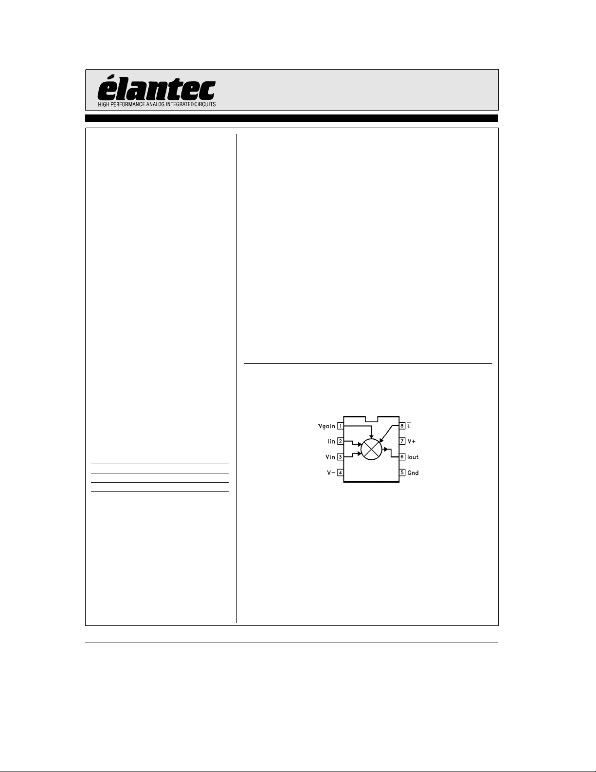
Connection Diagram
8-Pin DIP/SO
Ordering Information
Part No. Temp. Range Package Outline
EL2082CN 0§Ctoa75§C 8-Pin P-DIP MDP0031
EL2082CS 0§Ctoa75§C 8-Pin SO MDP0027
Note: All information contained in this data sheet has been carefully checked and is believed to be accurate as of the date of publication; however, this data sheet cannot be a ‘‘controlled document’’. Current revisions, if any, to these
specifications are maintained at the factory and are available upon your request. We recommend checking the revision level before finalization of your design documentation.
©
1992 Elantec, Inc.
Ý
2082– 1
Top View
Page 2
EL2082C
Current-Mode Multiplier
Absolute Maximum Ratings
a
V
S
V
IN,IOUT
VE,V
I
IN
Important Note:
All parameters having Min/Max specifications are guaranteed. The Test Level column indicates the specific device testing actually
performed during production and Quality inspection. Elantec performs most electrical tests using modern high-speed automatic test
equipment, specifically the LTX77 Series system. Unless otherwise noted, all tests are pulsed tests, therefore T
Test Level Test Procedure
Voltage between V
Voltage
Input Voltage
GAIN
Input Current
I 100% production tested and QA sample tested per QA test plan QCX0002.
II 100% production tested at T
III QA sample tested per QA test plan QCX0002.
IV Parameter is guaranteed (but not tested) by Design and Characterization Data.
V Parameter is typical value at T
T
MAX
and T
S
MIN
b
and V
S
A
per QA test plan QCX0002.
e
(T
25§C)
A
a
33V
g
V
b
e
A
S
1toa7V
g
5mA
25§C and QA sample tested at T
e
25§C for information purposes only.
P
D
T
A
T
J
T
ST
Maximum Power Dissipation See Curves
Operating Temperature Range 0§Ctoa75§C
Operating Junction Temperature 150§C
Storage Temperature
e
25§C,
A
b
65§Ctoa150§C
e
e
T
TA.
J
C
DC Electrical Characteristics
e
g
(V
S
Parameter Description Temp Min Typ Max Test Units
V
IO
I
OO
R
INI
V
CMRR
I
CMRR
V
PSRR
I
PSRR
I
BVIN
R
INV
Nlini Signal Nonlinearity; I
R
OUT
15V, V
e
G
1V, V
e
0.8V, V
E
OUT
e
0, V
e
e
0, I
IN
IN
Input Offset Voltage Full
Output Offset Current Full
IINInput Impedance; I
e
0, 0.35 mA Full 75 95 115 II X
IN
Voltage Common-Mode Rejection Ratio
eb
V
IN
10V,a10V
Offset Current Common-Mode Rejection
IN
eb
10V,a10V
Ratio, V
Offset Voltage Power Supply Rejection
e
S
g
5V tog15V
Ratio, V
Offset Current Power Supply Rejection
e
S
g
5V tog15V
Ratio, V
VINBias Current Full
IN
OUT
eb
10V,a10V Full 0.5 1.0 II MX
IN
eb
0.7 mA,
eb
10V,a10V Full 0.25 0.5 II MX
VINInput Impedance; V
b
0.35 mA, 0 mA,a0.35 mA,a0.7 mA
Output Impedance V
0)
Level
b
20 20 II mV
b
100 100 II mA
Full 45 55 II dB
Full 0.5 5 II mA/V
Full 60 80 II dB
Full 1 10 II mA/V
b
10 10 II mA
Full 0.10 0.4 II %
TDis 3.0in
2
Page 3
EL2082C
Current-Mode Multiplier
DC Electrical Characteristics
e
g
(V
S
15V, V
e
G
1V, V
e
0.8V, V
E
OUT
e
0, V
Ð Contd.
e
IN
0, I
e
0)
IN
Parameter Description Temp Min Typ Max Test Units
Level
V
V
A
OUT
IOG
I
Output Swing; V
e
4.0K
R
L
VOS, Gain Control, Extrapolated
from V
GAIN
Current Gain, I
e
GAIN
e
0.1V, 1V
g
350 mA Full 0.9 1.0 1.1 II mA/mA
IN
Nling Nonlinearity of Gain Control,
e
I
SO
V
V
I
LH
I
LL
I
ODIS
I
S
INH
INL
V
Input Isolation with V
E Logic High Level Full 2.0 II V
E Logic Low Level Full 0.8 II V
Input Current of E,V
Input Current of E,V
I
Supply Current Full 13 16 II mA
0.1V, 0.5V, 1V
GAIN
GAIN
e
E
e
E
, Disabled Ee2.0V Full
OUT
g
2V, I
2 mA,
IN
eb
0.1V Full
5V Full
0 Full
Full
Full
b
11
b
15 15 II mV
a
11 II V
Full 2 5 II %
b
b
b
b
80
96 II dB
50 50 II mA
50 50 II mA
g
10 II mA
AC Electrical Characteristics
e
(R
L
Parameter Description Min Typ Max
BW1 Current Mode Bandwidth
BW2
BWp Power, I
BWg Gain Control Bandwidth 20 V MHz
SRG Gain Control Slew Rate VGfrom 0.2V to 2V 12 V (mA/mA)/ms
T
REC
T
EN
T
DIS
D
G
D
P
25X,C
e
4 pF, C
L
IIN
e
2 pF, T
e
A
25§C, V
e
G
1V, V
e
g
15V)
S
Test
Level
b
3 dB 150 V MHz
g
0.1 dB 30 V MHz
e
1 mA p-p 150 V MHz
IN
Recovery Time from V
k
0 250 V ns
G
Enable Time from E Pin 200 V ns
Disable Time from E Pin 30 V ns
Differential Gain,
NTSC with I
eb
IN
Differential Phase,
NTSC with I
eb
IN
0.35 mA toa0.35 mA
0.35 mA toa0.35 mA
0.25 V %
0.05 V Degree
Units
TDis 2.8inTDis 2.4in
3
Page 4
EL2082C
Current-Mode Multiplier
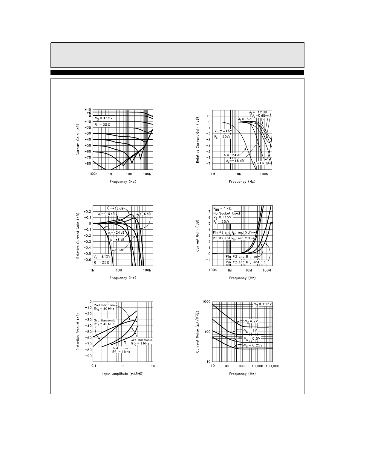
Typical Performance Curves
Current Gain vs
Frequency for Different Gains
Current Gain Flatness Voltage Input Mode
Current Gain
vs Frequency
Frequency Response in
Harmonic Distortion vs
Input Amplitude
Output Current Noise
vs Frequency
2082– 2
4
Page 5
EL2082C
Current-Mode Multiplier
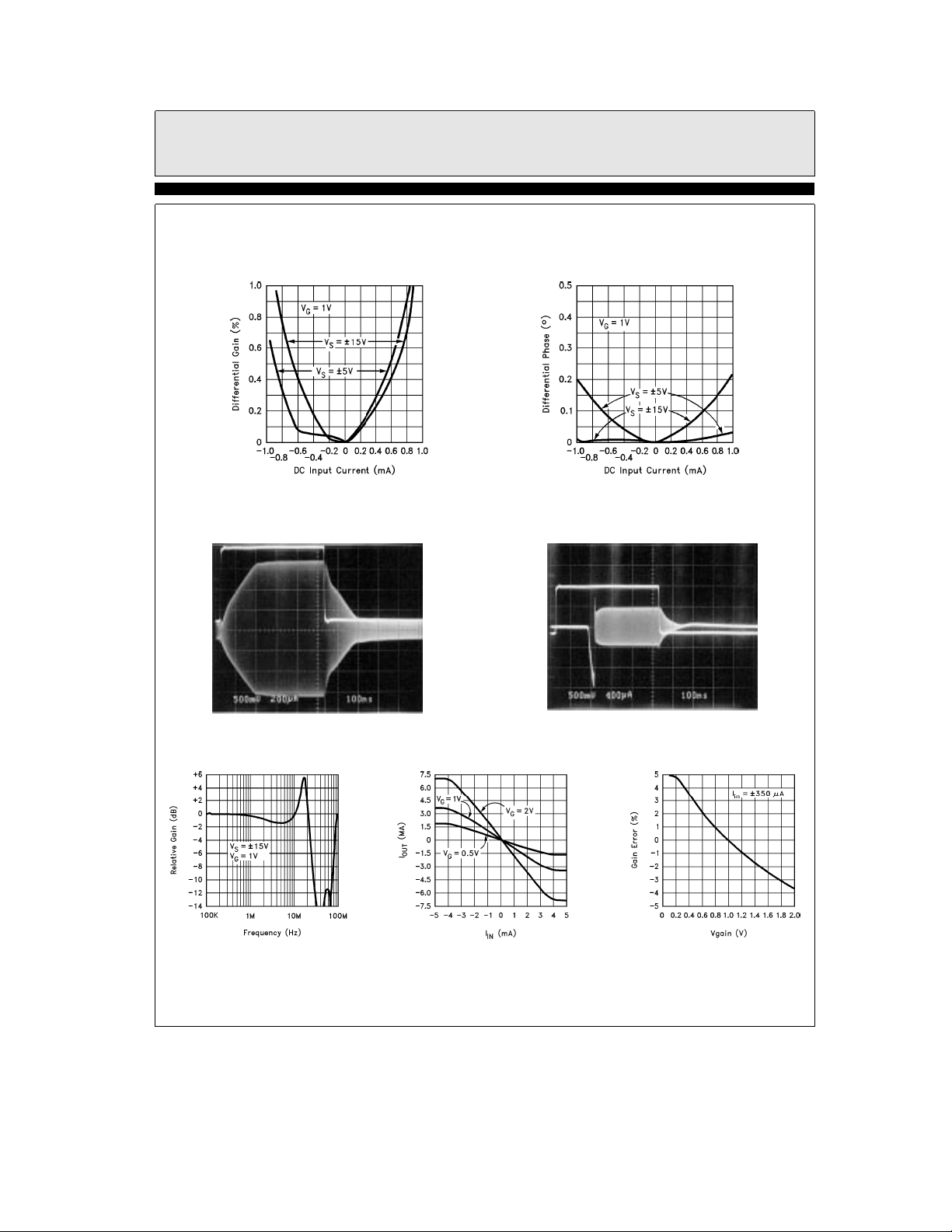
Typical Performance Curves
Differential Gain Error
vs DC Offset Current
Gain Pin Transient Response
Ð Contd.
Differential Phase Error vs
DC Offset Current
Gain Control Recovery From
eb
Vg
0.1V
2082– 3
Gain Control Pin
Frequency Response
I
2082– 4
OUT
vs I
2082– 5
Normalized Gain Error
IN
5
vs V
GAIN
Voltage
2082– 6
Page 6

EL2082C
Current-Mode Multiplier
Typical Performance Curves
Current Gain vs
Supply Voltage
Output Capacitance vs
Output Voltage
Ð Contd.
Current Gain vs
Temperature
Enable Pin Response
2082– 7
Supply Current vs
Supply Voltage
2082– 8
2082– 9
Supply Current vs
Die Temperature
2082– 10
6
Page 7

EL2082C
Current-Mode Multiplier
Typical Performance Curves
8-Pin Plastic DIP
Maximum Power Dissipation
vs Ambient Temperature
Ð Contd.
2082– 11
8-Lead SO
Maximum Power Dissipation
vs Ambient Temperature
2082– 12
Applications Information
The EL2082 is best thought of as a current-conveyor with variable current gain. A current input to the
I
pin will be replicated as a current driven out the I
IN
an input of 1 mA will produce an output current of 1 mA for V
produce an output of 2 mA for V
on V
, even onlyb20 mV, will yield very high signal attenuation.
GAIN
GAIN
e
2V. The useable V
The EL2082 in Conjunction with Op-Amps
This resistor-load circuit shows a simple method of converting voltage signals to currents and vice
versa:
pin, with a gain controlled by V
OUT
GAIN
e
GAIN
1V. An input of 1 mA will
range is zero toa2V. A negative level
GAIN
. Thus,
J#
2082– 13
a
R
R
F
G
R
J
G
EL2082aOp-Amp
Gain
V
GAIN
e
1V
R
L
a
R
95X
#
IN
RINwould typically be 1 kX for video level inputs, or 10 kX forg10V instrumentation signals. The
higher the value of R
(the lower the input current), the lower the distortion levels of the EL2082 will
IN
be. An approximate expression of the nonlinearity of the EL2082 is:
Nonlinearity (%)
e
0.3*IIN(mA)
2
Optimum input current level is a tradeoff between distortion and signal-to-noise-ratio. The distortion
and input range do not change appreciably with V
levels; distortion is set by input currents alone.
GAIN
7
Page 8

EL2082C
Current-Mode Multiplier
Applications Information
Ð Contd.
The output current could be terminated witha1kXload resistor to achieve a nominal voltage gain of 1
at the EL2082, but the I
practical total capacitance at I
, load, and stray capacitances would limit bandwidth greatly. The lowest
OUT
is about 12 pF, and this gives a 13 MHz bandwidth witha1kX
OUT
load. In the above example a 100X load is used for an upper limit of 130 MHz. The operational
amplifier gives a gain of
installing C
. This is a very small capacitor, typically 1 pf –2 pF, and it bolsters the gain above
IN
a
10 to bring the overall gain to unity. Wider bandwidth yet can be had by
100 MHz. Here is a table of results for this circuit used with various amplifiers:
Operational Power
Amplifier Supplies Rf Rg C
EL2020
EL2020
EL2130
EL2030
EL2090
EL2120
EL2120
EL2070
EL2071
EL2075
g
5V 620 68 Ð 34 MHz 5.6 MHz 0
g
15V 620 68 Ð 40 MHz 7.4 MHz 0
g
5V 620 68 Ð 73 MHz 11 MHz 1.0 dB
g
15V 620 68 Ð 93 MHz 12 MHz 1.3 dB
g
15V 240 27 Ð 60 MHz 10 MHz 0.5 dB
g
5V 220 24 Ð 57 MHz 10 MHz 0.4 dB
g
15V 220 24 Ð 65 MHz 11 MHz 0.3 dB
g
5V 200 22 2 pF 150 MHz 30 MHz 0.4 dB
g
5V 1.5K 240 2 pF 200 MHz 30 MHz 0
g
5V 620 68 2 pF 270 MHz 30 MHz 1.5 dB
IN
b
3 dB 0.1 dB
Bandwidth Bandwidth Peaking
Maximum bandwidth is maintained over a gain range ofa6tob16 dB; bandwidth drops at lower
gains. If wider gain range with full bandwidth is required, two or more EL2082’s can be cascaded with
the I
The EL2082 can also be used with an I
of one directly driving the IINof the next.
OUT
x
V operational circuit:
V
GAIN
eb
Inverting
EL2082aOp-Amp
Gain
1V
2082– 14
The circuit above gives a negative gain. The main concern of this connection involves the total I
R
F
a
R
95X
#
IN
J
OUT
and stray capacitances at the amplifier’s input. When using traditional op-amps, the pole caused by
these capacitances can make the amplifier less stable and even cause oscillations in amplifiers whose
gain-bandwidth is greater than 5 MHz. A typical cure is to add a capacitor Cf in the 2 pF – 10 pF range.
This will reduce overall bandwidth, so a capacitor C
ratio Cf/C
is made equal to RIN/Rf.
IN
can be added to regain frequency response. The
IN
8
Page 9

EL2082C
Current-Mode Multiplier
Applications Information
Ð Contd.
Current-feedback amplifiers eliminate this difficulty. Because their -input is a very low impedance,
capacitance at the summing point of an inverting operational circuit is far less troublesome. Here is a
table of results of various current-feedback circuits used in the inverting circuit:
Operational Power
Amplifier Supplies Rf R
EL2020
EL2020
EL2130
EL2030
EL2171
with the EL2171 the EL2082 had
g
5V 1k 910 Ð 29 MHz 4.3 MHz 0
g
15V 1k 910 Ð 34 MHz 5.3 MHz 0
g
5V 1k 910 Ð 61 MHz 9.7 MHz 0
g
15V 1k 910 Ð 82 MHz 12.3 MHz 0
g
5V 2k 1.8k 1k 114 MHz 11 MHz 1.2 dB
g
15V supplies and the EL2171 required a 150X output load.
IN
Rg Bandwidth Bandwidth Peaking
b
3 dB 0.1 dB
The EL2120 and EL2090 are suitable in this circuit but they are compensated for 300X feedback
resistors. R
would have to be reduced greatly to obtain unity gain and the increased signal currents
IN
would cause the EL2082 to display much increased distortion. They could be used if the input resistor
were maintained at 910X and Rf reduced for a
b
(/3 gain, or if Rfe1k and an overall bandwidth of
25 MHz were acceptable.
The EL2082 can also be used within an op-amp’s feedback loop:
Gain
eb
V
1V
GAIN
a
R
95X
F
R
#
J
IN
TDis 1.3in
EL2082 in feedback
inverting gain
2082– 15
With voltage-mode op-amps, the same concern about capacitance at the summing node exists, so Cf and
C
should be used. As before, current-feedback amplifiers tend to solve the problem. However, in this
IN
circuit the inherent phase lag of the EL2082 detracts from the phase margin of the op-amp, and some
overall bandwidth reduction may result. The EL2082 appears as a 3.0 ns delay, well past 100 MHz.
Thus, for a 20 MHz loop bandwidth, the EL2082 will subtract 20 MHz
c
3.0 nsc360 degreese21.6
degrees. The loop path should have at least 55 degrees of phase margin for low ringing in this connection. Loop bandwidth is always reduced by the ratio R
9
IN
/(R
a
Rf) with voltage mode op-amps.
IN
Page 10

EL2082C
Current-Mode Multiplier
Applications Information
Ð Contd.
Current-feedback op-amps again solve the summing-junction capacitance problem in this connection.
The loop bandwidth here becomes a matter of transimpedance over frequency and its phase characteristics. Unfortunately, this is generally poorly documented in amplifier data sheets. A rule of thumb is
that the transimpedance falls to the value of the recommended feedback resistor at a frequency of
F
b
3dB
/4 to F
b
3dB
/2, where F
is the unity-gain closed-loop bandwidth of the amplifier. The
b
3dB
phase margin of the op-amp is usually close to 90 degrees at this frequency.
In general, Rf is initially the recommended value for the particular amplifier and is then empirically
adjusted for amplifier stability at maximum V
, then RINis set for the overall circuit gain re-
GAIN
quired. Sometimes a very small Cf can be used to improve loop stability, but it often must be in series
with another resistor of value around Rf/2.
A virtue of placing the EL2082 in feedback is that the input-referred noise will drop as gain increases.
This is ideal for level controls that are used to set the output to a constant level for a variety of inputs
as well as AGC loops. Furthermore, the EL2082 has a relatively constant input signal amplitude for a
variety of input levels, and its distortion will be relatively constant and controllable by setting Rf. Note
that placing the EL2082 in the feedback path causes the circuit bandwidth to vary inversely with gain.
The next circuit shows use of the EL2082 in the feedback path of a non-inverting op-amp:
a
1V
R
95X
EL2082 in feedback
non-inverting gain
Gain
e
F
V
R
#
g
g
J
2082– 16
This example has the same virtues with regards to noise and distortion as the preceding circuit; and its
bandwidth shrinks with increasing gain as well. The typical 12 pF sum of EL2082 output capacitance in
parallel with stray capacitance necessitates the inclusion of Cf to prevent a feedback pole. Because of
this 12 pF capacitance at the op-amp -input, current-feedback op-amps will generally not be useable. As
before, the loop bandwidth and phase margin must accommodate the extra phase lag of the EL2082.
10
Page 11

EL2082C
Current-Mode Multiplier
Applications Information
Ð Contd.
Using the VINPin
The VINpin can be used instead of the IINpin so:
b
The VINpin used
as signal input
Gm
2082– 17
I
OUT
e
V
Vg
e
1v
IN
1
a
R
95X
#
J
g
This connection is useful when a high input impedance is required. There are a few caveats when using
the V
C
and can peak as much as 20 dB with large C
pin. The first is that VINhas a 250 V/ms slew rate limitation. The second is that the inevitable
IN
across Rg causes a gain zero and gain INCREASES above the 1/(2q C
STRAY
. A graph of gain vs. frequency for several C
STRAY
STRAY
Rg) frequency
STRAYS
is included in the typical performance curves. In general, if wide bandwidth and frequency flatness is
desired, the I
The V
IN
be rejected. The next schematic shows the EL2082 V
pin should be used.
IN
pin does make an excellent ground reference pin, for instance when low-frequency noise is to
pin rejecting possible 60 Hz hum induced on an
IN
RF input cable:
Using the VINpin
as a ground reference
to reject hum and noise
2082– 18
This example shows VINrejecting low-frequency field-induced noise but not adding peaking since the
0.01 mF bypass capacitor shunts high-frequency signals to local ground.
Reactive Couplings with the EL2082
The following sketch is an excerpt of a receiver IF amplifier showing methods of connecting the
EL2082 to reactive networks:
Example Reactive
Couplings with EL2082’s
11
2082– 19
Page 12

EL2082C
Current-Mode Multiplier
Applications Information
The I
pin of the EL2082 looks like 95X well past 100 MHz, and the output looks like a simple
IN
Ð Contd.
current-source in parallel with about 5 pF. There is no particular problem with any resistance or
reactance connected to I
required a few hundred ohm terminating impedance. The impedance of the I
IN
or I
. The mixer output is generally sent to a crystal filter, which
OUT
pin of the first EL2082
IN
is transformed to about 400X by the 2:1 transformer T1. The two EL2082’s are used as variable-gain IF
amplifiers, with small gains offered by each. The output of the first EL2082 is coupled to the second by
the resonant matching network L1 –C1. ForaQof5,Xc1
impedance seen at the first EL2082’s I
will be about Q
OUT
mation alone the first gain cell delivers 28 dB of gain at Vg
e
x11e5c95X, approximately. The
2
c
95X, or 2.5k, and by impedance transfor-
e
1V. More gain cells can be used for a
wider range of (calibrated) AGC compliance.
input can be used as a high-speed noise blanker gate.
The E
Linearized Fader/Gain Control
The following circuit is an example of placing two EL2082’s in the feedback network of an op-amp to
significantly reduce their distortions:
Linearized Gain Control/Fader
Dual EL2082 Fader with EL2030
NTSC Differential Gain Error
2082– 21
e
V
where OsKs1
Dual EL2082 Fader with EL2030
NTSC Differential Phase Error
12
OUT
a(1b
2082– 20
K#V
K)#V
A
B
2082– 22
Page 13

EL2082C
Current-Mode Multiplier
Applications Information
The circuit sums two inputs A and B, such that the sum of their respective path gains is unity, as
controlled by the potentiometer. When the potentiometer’s wiper is fully down, the slightly negative
voltage at the Vg of the B-side EL2082 cuts off the B signal to better than 70 dB attenuation at
3.58 MHz. The A-side EL2082 is at unity gain, so the only (error) signal presented to the op-amp’s -input is the same (error) signal at the I
error signal required by the op-amp is very small, even at video frequencies, the current through the Aside EL2082 is small and distortion is minimized.
At 50% potentiometer setting, equal error output signals flow from the EL2082’s, since the op-amp still
requires little net -input current. The EL2082’s essentially buck each other to establish an output, and
50% gain occurs for both the A and B inputs. The EL2082’s now contribute distortion, but less than in
previous connections. The op-amp sees a constant 1k feedback resistor regardless of potentiometer
setting, so frequency response is stable for all gain settings.
A single-input gain control is implemented by simply grounding B
Distortion can be improved by increasing the input resistors to lower signal currents. This will lower
the overall gain accordingly, but will not affect bandwidth, which is dependent upon the feedback
resistors. Reducing the signal input amplitude is an analagous tactic, but the noise floor will effectively
rise.
Another strategy to reduce distortion in video systems is to use DC restoration circuitry, such as the
EL2090 ahead of the fader inputs to reduce the range of signals to be dealt with; the
possible range of inputs (due to capacitor coupling) would be changed to a stabilized
span.
The EL2020, EL2030, and EL2120 (at reduced bandwidth since it is compensated for 300X feedback
resistors) all give the same video performance at NTSC operation.
Ð Contd.
of the A-side EL2082. The circuit thus outputs -AIN. Since the
IN
.
IN
b
0.7V toa0.7V
b
0.35V toa0.35V
Variable Filters
This circuit is the familiar state-variable configuration, similar to the bi-quad:
Voltage Tuneable Bi-Quad Filter
Vg
e
F
0
1V
1
2q (Ra95X)C
#
J
13
2082– 23
Page 14

EL2082C
Current-Mode Multiplier
Applications Information
Ð Contd.
Frequency-setting resistors R are each effectively adjusted in value by an EL2082 to effect voltage-variable tuning. Two gain controls yields a linear frequency adjustment; using one gives a square-root-ofcontrol voltage tuning. The EL2082’s could be placed in series with the integrator capacitors instead to
yield a tuning proportional to 1/Vg.
The next circuit is one of a new class of ‘‘CCII’’ filters that use the current-conveyor element. Basic
information is available in the April 1991, volume 38, number 4 edition of the IEEE Transactions on
Circuits and Systems journal, pages 456 through 461 of the article ‘‘The Single CCII Biquads with
High-Input Impedance’’, by Shen-Iuan Liu and Hen-Wai Tsao.
e
f
160 kHz
O
‘‘CCII’’ Class Filter
2082– 24
This interesting filter uses the current output of the EL2082 to generate a bandpass voltage output and
the intermediate node provides a second-order low-pass filter output. Both outputs should be buffered
so as not to warp characteristics, although the V
of cascaded filters. The V
The resistor at I
could serve as the frequency trim, and Q trimmed subsequently with V
OUT
input acts a s a Q and peaking adjust point around the nominal 1V value.
GAIN
of the next EL2082 can be driven directly in the case
IN
GAIN
.
Negative Components
The following circuit converts a component or two-terminal network to a variable and even negative
replica of that impedance:
Variable or Negative Impedance Converter
Z
IN
(Za95X)
e
(1bVg/1V)
2082– 25
14
Page 15

EL2082C
Current-Mode Multiplier
Applications Information
Ð Contd.
A negative impedance is simply an impedance whose current flows reverse to the normal sense. In the
above circuit, the current through Z is replicated by the EL2082 and inverted (I
the sense of I
impedance is simply Z
the input and the input impedance is ‘‘infinite’’. When Vg
through Z is summed with the input resulting in an input impedance of
in the EL2082) and summed back to the input. When Vge0orVgk0, the input
IN
a
95X. When Vge1V, the negative of the current through Z is summed with
e
2V, twice the negative of the current
b
Z–95X.
flows inverted to
OUT
Thus variable capacitors can be simulated by substituting the capacitor as Z. ‘‘Negative’’ capacitors
result for Vg
l
1V, and capacitance needs to be present in parallel with the input to prevent oscillations.
Inductors or complicated networks also work for Z, but a net negative impedance will result in oscillations.
EL2082 Macromodel
This macromodel has been designed to work with PSPICE (copywritten by the Microsim Corporation).
E500 buffers in the V
supplies the non-linearity of the current channel and replicates the I
voltage. R500 and C500 provide the bandwidth limitation on the current signal. E502 supplies the
V
non-linearity and drives the L501/R501/C501 to shape the gain control frequency response.
GAIN
E503 does the actual gain-control multiplication, and drives delay line T500 to better simulate the
actual phase characteristics of the part G500 creates the current output, and R
proper output parasitics.
voltage and presents it to the R
IN
resistor to emulate the IINpin. E501
INI
Schematic of
EL2082 Macromodel
current to a ground referenced
IN
with C
OUT
OUT
provide
2082– 26
The model is good at frequency and linearity estimates around Vge1V and nominal temperatures, but
has several limitations:
The Vg channel does not give zero gain for
k
Vg
Vg
0; the output gain reverses –don’t use
k
0
The Vg channel is not slew limited
Frequency response does not vary with supply
The V
Noise is not modeled
Temperature effects are not modeled
CMRR and PSRR are not modeled
Frequency response does not vary with Vg
channel is not slew limited
IN
voltage
Unfortunately, the polynomial expressions and two-input multiplication may not be available on every
simulator. Results have been confirmed by laboratory results in many situations with this macromodel,
within its capabilities.
15
Page 16

EL2082C
Current-Mode Multiplier
EL2082CJanuary 1996, Rev D
EL2082 Macromodel
*: Vgain
*
*
*
*
.SUBCKT EL2082macro (1 2 3 45678)
***
*** I-to-I gain cell macromodel ***
***
******
Cini202P
C500 502 0 0.9845P
C501 505 0 1000P
Cout605P
******
L501 503 504 0.1U
******
Rsilly1101E9
Rsilly2 505 0 1E9
Rini 2 500 95
Rinv 3 0 2Meg
Rout 6 0 1Meg
R500 501 502 1000
R501 504 505 5
R502 506 507 50
R503 508 0 50
******
E500 5000301
E501 501 0 POLY(1) (2,500) 0 2 0 -.8
E502 503 0 POLY(1) (1,0) 0 1.05 -.05
E503 506 0 POLY(2) (505,0) (502,0)00001
G500 6 0 508 0 -0.0105
T500 508 0 507 0 Z0450 TD41.95N
******
.ENDS
Iin
l
ll
lll
Vin
Iout
lll l
TABWIDE
TDis 4.1in
General Disclaimer
Specifications contained in this data sheet are in effect as of the publication date shown. Elantec, Inc. reserves the right to make changes
in the circuitry or specifications contained herein at any time without notice. Elantec, Inc. assumes no responsibility for the use of any
circuits described herein and makes no representations that they are free from patent infringement.
WARNING Ð Life Support Policy
Elantec, Inc. products are not authorized for and should not be
used within Life Support Systems without the specific written
consent of Elantec, Inc. Life Support systems are equipment in-
Elantec, Inc.
1996 Tarob Court
Milpitas, CA 95035
Telephone: (408) 945-1323
(800) 333-6314
Fax: (408) 945-9305
European Office: 44-71-482-4596
tended to support or sustain life and whose failure to perform
when properly used in accordance with instructions provided can
be reasonably expected to result in significant personal injury or
death. Users contemplating application of Elantec, Inc. products
in Life Support Systems are requested to contact Elantec, Inc.
factory headquarters to establish suitable terms & conditions for
these applications. Elantec, Inc.’s warranty is limited to replacement of defective components and does not cover injury to persons or property or other consequential damages.
Printed in U.S.A.16
 Loading...