

Page 1
EL2075C
2GHz GBWP Gain-of-10 Stable Operational Amplifier
EL2075C
Features
• 2GHz gain-bandwidth product
• Gain-of-10 stable
• Conventional voltage-feedback
topology
• Low offset voltage = 200µV
• Low bias current = 2µA
• Low offset current = 0.1µA
• Output current = 50mA over
temperature
• Fast settling = 13ns to 0.1%
Applications
• Active filters/integrators
• High-speed signal processing
• ADC/DAC buffers
• Pulse/RF amplifiers
• Pin diode receivers
• Log amplifiers
• Photo multiplier amplifiers
• High speed sample-and-holds
Ordering Information
Part No. Temp. Range Package Outline #
EL2075CN 0°C to +75°C 8-Pin P-DIP MDP0031
EL2075CS 0°C to +75°C 8-Lead SO MDP0027
General Description
The EL2075C is a precision voltage-feedback amplifier featuring a
2GHz gain-bandwidth product, fast settling time, excellent differential
gain and differential phase performance, and a minimum of 50mA output current drive over temperature.
The EL2075C is gain-of-10 stable with a -3dB bandwidth of 400MHz
at AV = +10. It has a very low 200µV of input offset voltage, only 2µA
of input bias current, and a fully symmetrical differential input. Like
all voltage-feedback operational amplifiers, the EL2075C allows the
use of reactive or non-linear components in the feedback loop. This
combination of speed and versatility makes the EL2075C the ideal
choice for all op-amp applications at a gain of 10 or greater requiring
high speed and precision, including active filters, integrators, sampleand-holds, and log amps. The low distortion, high output current, and
fast settling makes the EL2075C an ideal amplifier for signal-processing and digitizing systems.
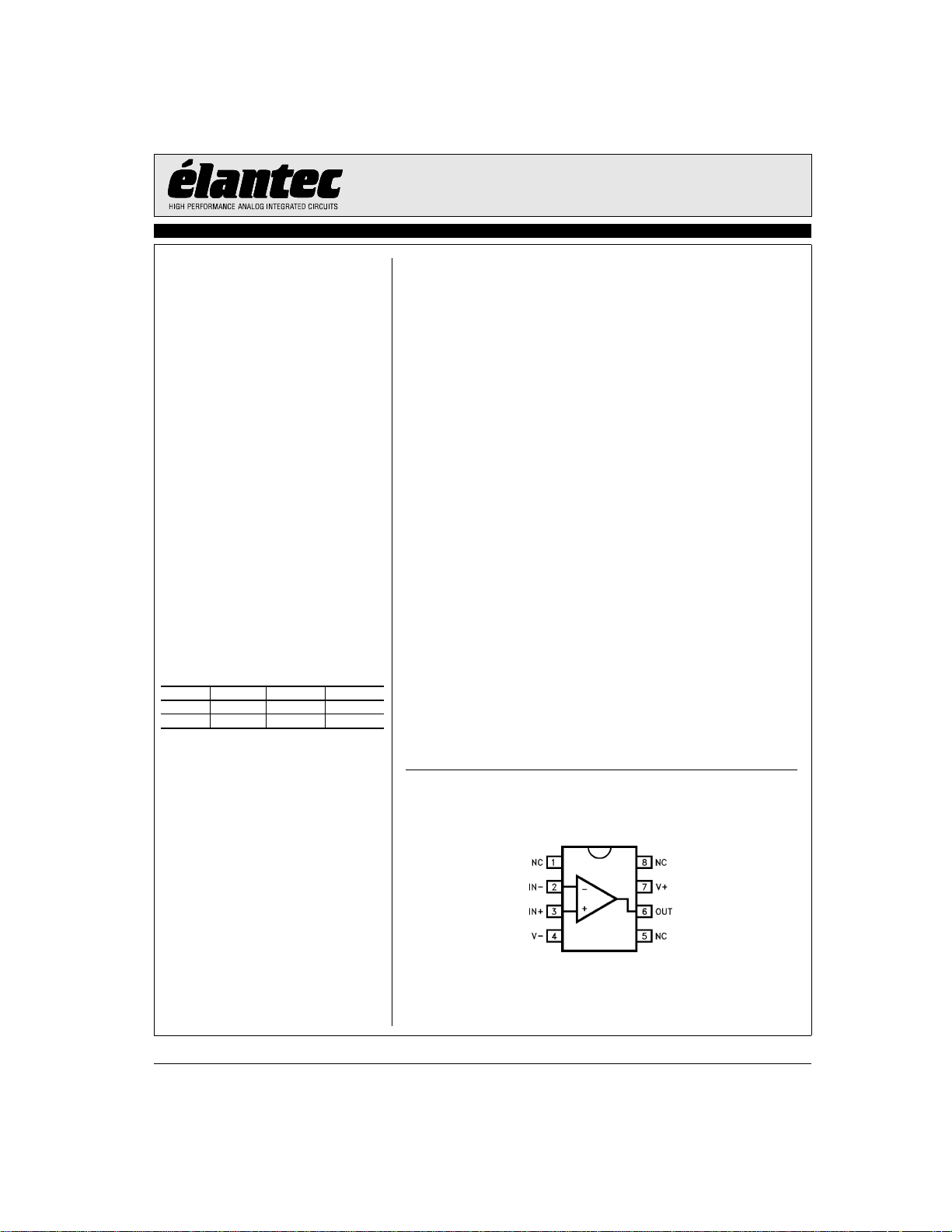
Connection Diagrams
DIP and SO Package
Note: All information contained in this data sheet has been carefully checked and is believed to be accurate as of the date of publication; however, this data sheet cannot be a “controlled document”. Current revisions, if any, to these
specifications are maintained at the factory and are available upon your request. We recommend checking the revision level before finalization of your design documentation.
© 2001 Elantec Semiconductor, Inc.
September 26, 2001
Page 2
EL2075C
2GHz GBWP Gain-of-10 Stable Operational Amplifier
EL2075C
Absolute Maximum Ratings (T
Supply Voltage (VS) ±7V
Output Current Output is short-circuit protected to ground, however,
maximum reliability is obtained if I
Common-Mode Input ±V
Differential Input Voltage 5V
Thermal Resistance θJA = 95°C/W P-DIP
does not exceed 70mA.
OUT
= 25°C)
A
Operating Temperature 0°C to +75°C
θJA = 175°C/W SO-8
Junction Temperature 175°C
S
Storage Temperature -60°C to +150°C
Note: See EL2071/EL2171 for Thermal Impedance curves.
Important Note:
All parameters having Min/Max specifications are guaranteed. Typ values are for information purposes only. Unless otherwise noted, all tests are at the
specified temperature and are pulsed tests, therefore: TJ = TC = TA.
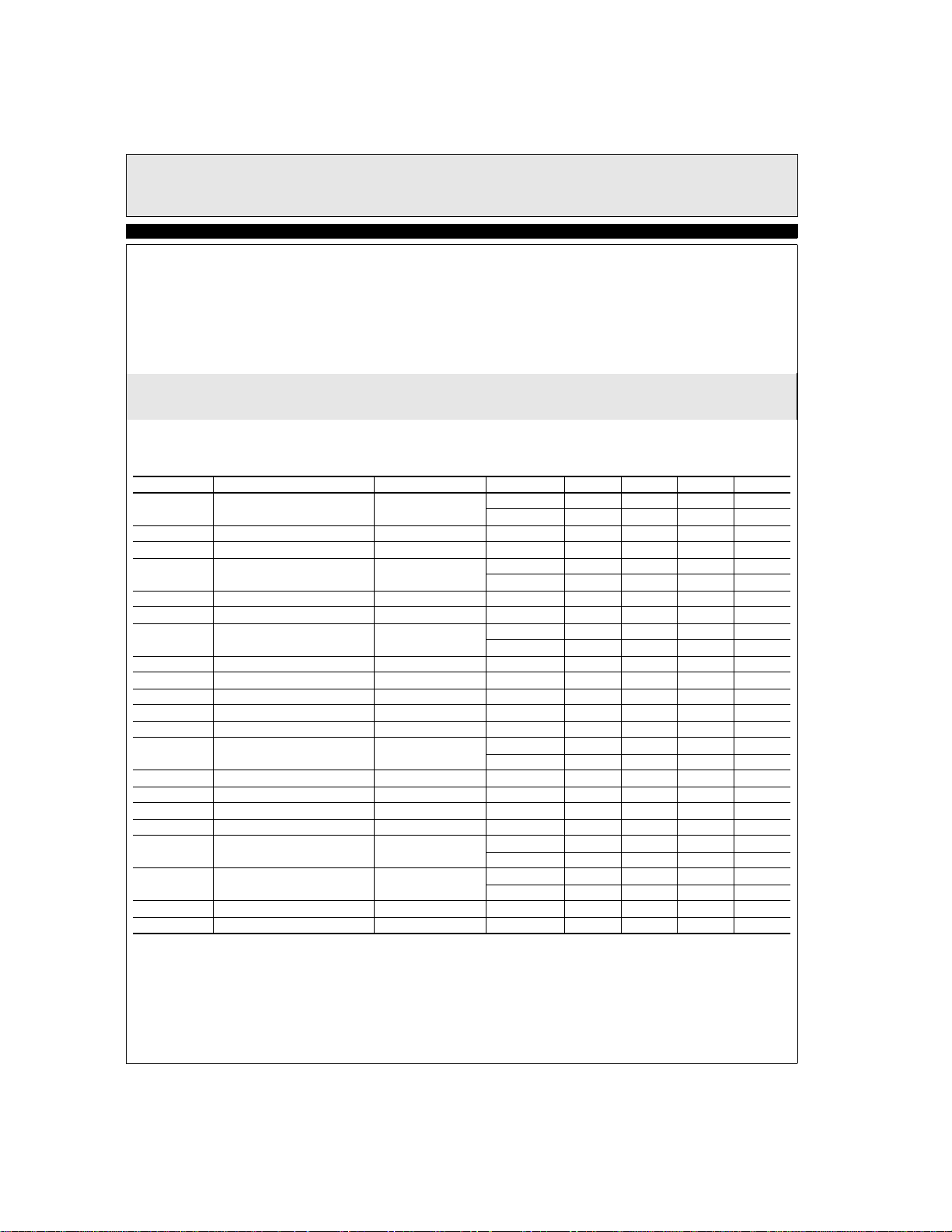
Open Loop DC Electrical Characteristics
VS = ±5V, R
V
TCV
I
B
I
OS
PSRR Power Supply Rejection Ratio
CMRR Common Mode Rejection Ratio
I
S
RIN (diff) RIN (Differential) Open-Loop 25°C 15 kΩ
CIN (diff) CIN (Differential) Open-Loop 25°C 1 pF
RIN (cm) RIN (Common-Mode) 25°C 1 MΩ
CIN (cm) CIN (Common-Mode) 25°C 1 pF
R
CMIR Common-Mode Input
I
OUT
V
V
V
A
A
eN@ > 1MHz Noise Voltage 1–100MHz 25°C 2.3 nV/√Hz
iN@ > 100 kHz Noise Current 100k–100MHz 25°C 3.2 pA/√Hz
= 100Ω, unless otherwise specified
L
Parameter Description Test Conditions Temp Min Typ Max Unit
OS
OS
Input Offset Voltage VCM = 0V 25°C 0.2 1 mV
T
Average Offset Voltage Drift
, T
MIN
[1]
MAX
All 8 µV/°C
2.5 mV
Input Bias Current VCM = 0V All 2 6 µA
Input Offset Current VCM = 0V 25°C 0.1 1 µA
T
, T
MIN
[2]
[3]
MAX
All 70 90 dB
All 70 90 dB
2 µA
Supply Current—Quiescent No Load 25°C 21 25 mA
T
OUT
, T
MIN
MAX
Output Resistance 25°C 50 mΩ
25 mA
25°C ±3 ±3.5 V
Range
T
MIN
, T
MAX
±2.5 V
Output Current All 50 70 mA
OUT
100 Output Voltage Swing 100Ω All ±3 ±3.6 V
OUT
50 Output Voltage Swing 50Ω All ±2.5 ±3.4 V
OUT
100 Open-Loop Gain 100Ω 25°C 1000 2800 V/V
VOL
50 Open-Loop Gain 50Ω 25°C 800 2300 V/V
VOL
1. Measured from T
Output Voltage Swing No Load All ±3.5 ±4 V
T
MIN
, T
MIN
MAX
T
, T
MIN
MAX
, T
.
MAX
800 V/V
600 V/V
2. ±VCC = ±4.5V to 5.5V.
3. ±VIN = ±2.5V, V
OUT
= 0V
2
Page 3
EL2075C
2GHz GBWP Gain-of-10 Stable Operational Amplifier
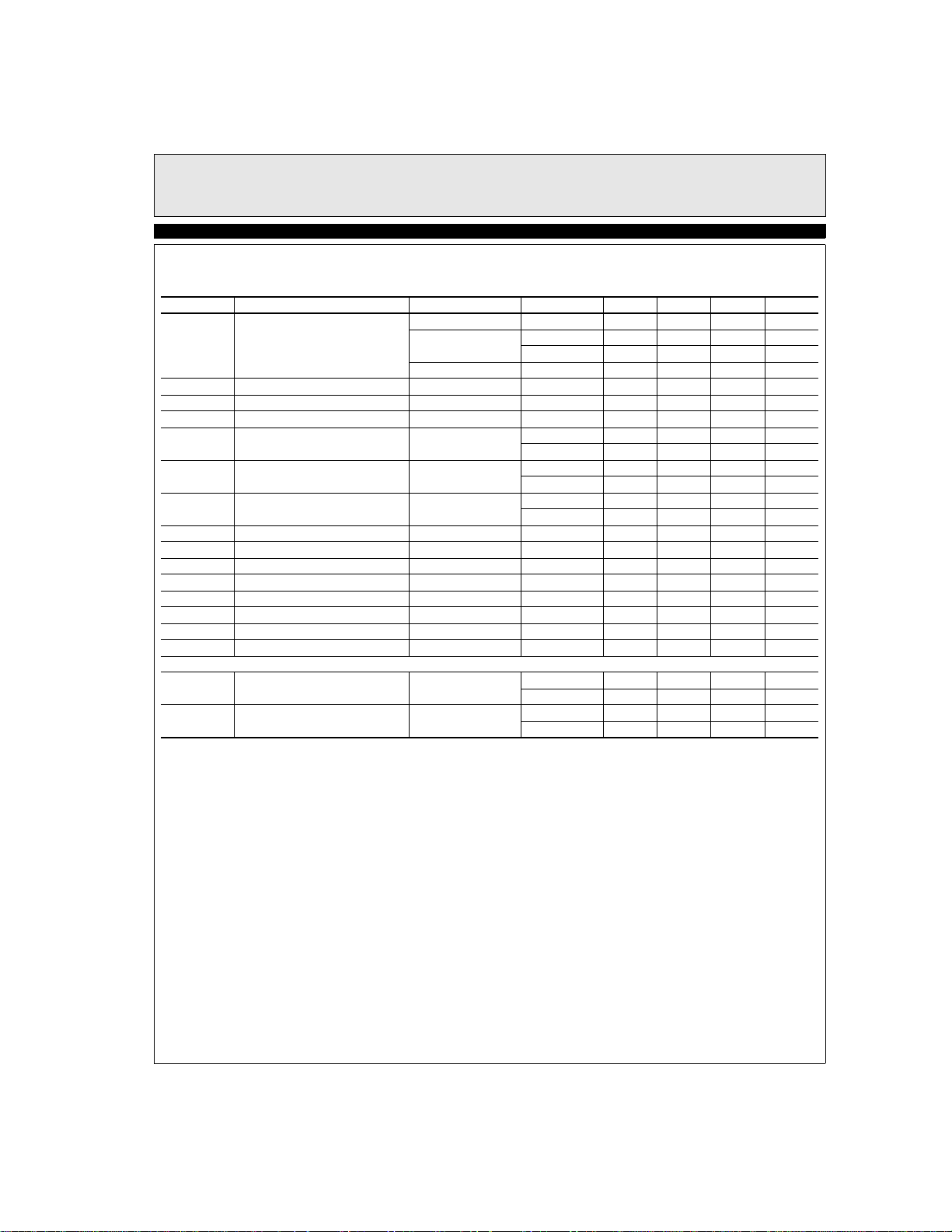
Closed Loop AC Electrical Characteristics
VS = ±5V, A
SSBW -3dB Bandwidth
GBWP Gain-Bandwidth Product AV = +100 25°C 2.0 GHz
LSBWa -3dB Bandwidth V
LSBWb -3dB Bandwidth V
GFPL Peaking (<50MHz) V
GFPH Peaking (>50MHz) V
GFR Rolloff (<100MHz) V
LPD Linear Phase Deviation (<100MHz) V
PM Phase Margin AV = +10 25°C 60 °
tr1, tf1 Rise Time, Fall Time 0.4V Step, AV = +10 25°C 1.2 ns
tr2, tf2 Rise Time, Fall Time 5V Step, AV = +10 25°C 6 ns
ts1 Settling to 0.1% (AV = -20) 2V Step 25°C 13 ns
ts2 Settling to 0.01% (AV = -20) 2V Step 25°C 25 ns
OS Overshoot 2V Step, AV = +10 25°C 10 %
SR Slew Rate 2V Step, AV = +10 All 500 800 V/µs
DISTORTION
HD2 2nd Harmonic Distortion @ 20MHz, AV = +20 25°C -40 -30 dBc
HD3 3rd Harmonic Distortion @ 20MHz, AV = +20 25°C -65 -50 dBc
1. Large-signal bandwidth calculated using LSBW = Slew Rate / (2¼ • V
2. All distortion measurements are made with V
= +20, Rf = 1500Ω, RL = 100Ω unless otherwise specified.
V
Parameter Description Test Conditions Temp Min Typ Max Unit
AV = +10 25°C 400 MHz
(V
= 0.4VPP)
OUT
AV = +20 25°C 150 200 MHz
T
MIN
, T
MAX
125 MHz
AV = +50 25°C 40 MHz
[1]
= 2V
OUT
PP
[1]
= 5V
OUT
PP
= 0.4V
OUT
PP
= 0.4V
OUT
PP
= 0.4V
OUT
PP
= 0.4V
OUT
PP
[2]
).
= 2VPP, RL = 100¾.
OUT
PEAK
All 80 128 MHz
All 32 50 MHz
25°C 0 0.5 dB
T
MIN
, T
MAX
0.5 dB
25°C 0 1 dB
T
MIN
, T
MAX
1 dB
25°C 0.1 0.5 dB
T
MIN
, T
MAX
0.5 dB
All 1 1.8 °
T
, T
MIN
MAX
T
, T
MIN
MAX
-30 dBc
-50 dBc
EL2075C
3
Page 4
EL2075C
2GHz GBWP Gain-of-10 Stable Operational Amplifier
EL2075C
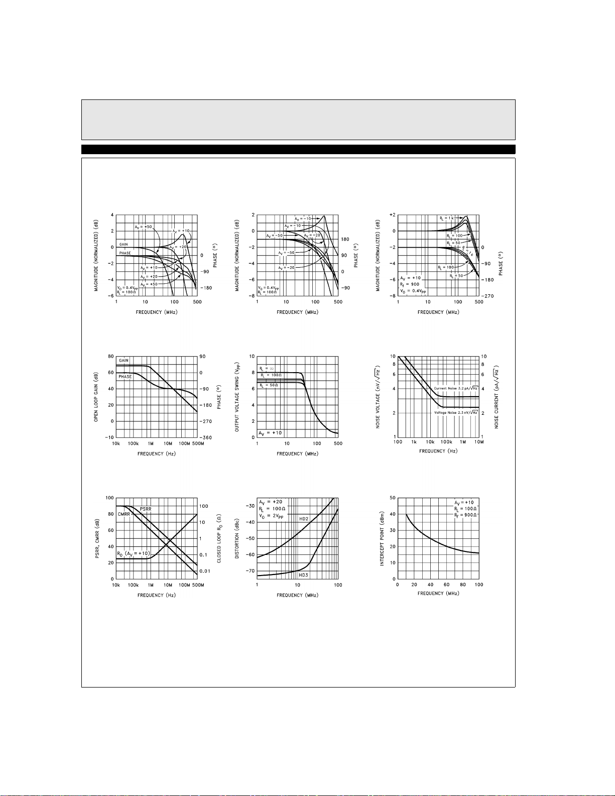
Typical Performance Curves
Non-Inverting
Frequency Response
Open Loop Gain
and Phase
PSRR, CMRR, and Closed-Loop
RO Frequency
Inverting Frequency Response Frequency Response
vs Frequency
2nd and 3rd Harmonic
Distortion vs Frequency
for Various RLs
Equivalent Input NoiseOutput Voltage Swing
2-Tone, 3rd Order
Intermodulation Intercept
4
Page 5

EL2075C
2GHz GBWP Gain-of-10 Stable Operational Amplifier
EL2075C
Series Resistor and Resulting
Bandwidth vs Capacitive Load
Common-Mode Rejection Ratio vs
Input Common-Mode Voltage
Bias and Offset Current
vs Temperature
Settling Time vs
Output Voltage Change
Bias and Offset Current vs
Input Common-Mode Voltage
Offset Voltage
vs Temperature
Settling Time vs
Closed-Loop Gain
Supply Current
vs Temperature
A
, PSRR, and CMRR
VOL
vs Temperature
5
Page 6

EL2075C
2GHz GBWP Gain-of-10 Stable Operational Amplifier
EL2075C
Small Signal Transient Response Large Signal Transient Response
6
Page 7

Equivalent Circuit
EL2075C
EL2075C
2GHz GBWP Gain-of-10 Stable Operational Amplifier
Burn-In Circuit
All Packages Use The Same Schematic
7
Page 8

EL2075C
2GHz GBWP Gain-of-10 Stable Operational Amplifier
EL2075C
Applications Information
Product Description
The EL2075C is a wideband monolithic operational
amplifier built on a high-speed complementary bipolar
process. The EL2075C uses a classical voltage-feedback
topology which allows it to be used in a variety of applications requiring a noise gain ≥10 where currentfeedback amplifiers are not appropriate because of
restrictions placed upon the feedback element used with
the amplifier. The conventional topology of the
EL2075C allows, for example, a capacitor to be placed
in the feedback path, making it an excellent choice for
applications such as active filters, sample-and-holds, or
integrators. Similarly, because of the ability to use
diodes in the feedback network, the EL2075C is an
excellent choice for applications such as log amplifiers.
The EL2075C also has excellent DC specifications:
200µV, VOS, 2µA IB, 0.1µA IOS, and 90dB of CMRR.
These specifications allow the EL2075C to be used in
DC-sensitive applications such as difference amplifiers.
Furthermore, the current noise of the EL2075C is only
3.2 pA/√Hz, making it an excellent choice for high-sensitivity transimpedance amplifier configurations.
Gain-Bandwidth Product
The EL2075C has a gain-bandwidth product of 2GHz.
For gains greater than 40, its closed-loop -3dB bandwidth
is approximately equal to the gain-bandwidth product
divided by the noise gain of the circuit. For gains less
than 40, higher-order poles in the amplifier's transfer
function contribute to even higher closed loop bandwidths. For example, the EL2075C has a -3dB bandwidth
of 400MHz at a gain of +10, dropping to 200MHz at a
gain of +20. It is important to note that the EL2075C has
been designed so that this “extra” bandwidth in low-gain
applications does not come at the expense of stability. As
seen in the typical performance curves, the EL2075C in a
gain of +10 only exhibits 1.5dB of peaking with a 100Ω
load.
Output Drive Capability
The EL2075C has been optimized to drive 50Ω and 75Ω
loads. It can easily drive 6VPP into a 50Ω load. This high
output drive capability makes the EL2075C an ideal
choice for RF and IF applications. Furthermore, the current drive of the EL2075C remains a minimum of 50mA
at low temperatures. The EL2075C is current-limited at
the output, allowing it to withstand momentary shorts to
ground. However, power dissipation with the output
shorted can be in excess of the power-dissipation capabilities of the package.
Capacitive Loads
Although the EL2075C has been optimized to drive
resistive loads as low as 50Ω, capacitive loads will
decrease the amplifier's phase margin which may result
in peaking, overshoot, and possible oscillation. For optimum AC performance, capacitive loads should be
reduced as much as possible or isolated via a series output resistor. Coax lines can be driven, as long as they are
terminated with their characteristic impedance. When
properly terminated, the capacitance of coaxial cable
will not add to the capacitive load seen by the amplifier.
Capacitive loads greater than 10pF should be buffered
with a series resistor (Rs) to isolate the load capacitance
from the amplifier output. A curve of recommended Rs
vs Cload has been included for reference. Values of Rs
were chosen to maximize resulting bandwidth without
additional peaking.
Printed-Circuit Layout
As with any high-frequency device, good PCB layout is
necessary for optimum performance. Ground-plane construction is highly recommended, as is good power
supply bypassing. A 1µF–10µF tantalum capacitor is
recommended in parallel with a 0.01µF ceramic capacitor. All lead lengths should be as short as possible, and
all bypass capacitors should be as close to the device
pins as possible. Parasitic capacitances should be kept to
an absolute minimum at both inputs and at the output.
Resistor values should be kept under 1000Ω to 2000Ω
because of the RC time constants associated with the
parasitic capacitance. Metal-film and carbon resistors
are both acceptable, use of wire-wound resistors is not
recommended because of parasitic inductance. Similarly, capacitors should be low-inductance for best
performance. If possible, solder the EL2075C directly to
the PC board without a socket. Even high quality sockets
8
Page 9

EL2075C
2GHz GBWP Gain-of-10 Stable Operational Amplifier
EL2075C
add parasitic capacitance and inductance which can
potentially degrade performance. Because of the degradation of AC performance due to parasitics, the use of
surface-mount components (resistors, capacitors, etc.) is
also recommended.
9
Page 10

EL2075C
2GHz GBWP Gain-of-10 Stable Operational Amplifier
EL2075C
EL2075C Macromodel
*
* Connections: input
* | -input
* | | +Vsupply
* | | | -Vsupply
* | | | | output
* | | | | |
.subckt M2075C 3 2 7 4 6
*
*Input Stage
*
ie 37 4 1mA
r6 36 37 15
r7 38 37 15
rc1 7 30 200
rc2 7 39 200
q1 30 3 36 qn
q2 39 2 38 qna
ediff 33 0 39 30 1
rdiff 33 0 1 Meg
*
* Compensation Section
*
ga 0 34 33 0 2m
rh 34 0 500K
ch 34 0 0.4 pF
rc 34 40 50
cc 40 0 0.05 pF
*
* Poles
*
ep 41 0 40 0 1
rpa 41 42 250
cpa 42 0 0.8 pF
rpb 42 43 50
cpb 43 0 0.5 pF
*
* Output Stage
*
ios1 7 50 3.0mA
ios2 51 4 3.0mA
q3 4 43 50 qp
q4 7 43 51 qn
q5 7 50 52 qn
q6 4 51 53 qp
ros1 52 6 2
ros2 6 53 2
*
* Power Supply Current
*
ips 7 4 11.4mA
*
* Models
*
.model qna npn(is800e-18 bf170 tf0.2ns)
.model qn npn(is810e-18 bf200 tf0.2ns)
.model qp pnp(is800e-18 bf200 tf0.2ns)
.ends
10
Page 11

EL2075C
2GHz GBWP Gain-of-10 Stable Operational Amplifier
EL2075C
General Disclaimer
Specifications contained in this data sheet are in effect as of the publication date shown. Elantec, Inc. reserves the right to make changes in the circuitry or specifications contained herein at any time without notice. Elantec, Inc. assumes no responsibility for the use of any circuits described
herein and makes no representations that they are free from patent infringement.
WARNING - Life Support Policy
Elantec, Inc. products are not authorized for and should not be used
within Life Support Systems without the specific written consent of
Elantec, Inc. Life Support systems are equipment intended to sup-
Elantec Semiconductor, Inc.
675 Trade Zone Blvd.
Milpitas, CA 95035
Telephone: (408) 945-1323
(888) ELANTEC
Fax: (408) 945-9305
European Office: +44-118-977-6020
Japan Technical Center: +81-45-682-5820
port or sustain life and whose failure to perform when properly used
in accordance with instructions provided can be reasonably
expected to result in significant personal injury or death. Users contemplating application of Elantec, Inc. Products in Life Support
Systems are requested to contact Elantec, Inc. factory headquarters
to establish suitable terms & conditions for these applications. Elantec, Inc.’s warranty is limited to replacement of defective
components and does not cover injury to persons or property or
other consequential damages.
September 26, 2001
11
Printed in U.S.A.
 Loading...