

EL2072C
730 MHz Closed Loop Buffer
EL2072C December 1995 Rev E
Features
# 730 MHzb3 dB bandwidth
(0.5 V
PP
)
# 5 ns settling to 0.2%
e
S
g
5V@15 mA
# V
# Low distortion: HD2, HD3 of
b
65 dBc at 20 MHz
# Overload/short-circuit protected
# Closed-loop, unity gain
# Low cost
# Direct replacement for CLC110
Applications
# Video buffer
# Video distribution
# HDTV buffer
# High-speed A/D buffer
# Photodiode, CCD preamps
# IF processors
# High-speed communications
Ordering Information
Part No. Temp. Range Package Outline
EL2072CNb40§Ctoa85§C 8-Pin P-DIP MDP0031
EL2072CSb40§Ctoa85§C 8-Pin SO MDP0027
General Description
The EL2072 is a wide bandwidth, fast settling monolithic buffer
built using an advanced complementary bipolar process. This
buffer is closed loop to achieve lower output impedance and
higher gain accuracy. Designed for closed-loop unity gain, the
EL2072 has a 730 MHz
b
3 dB bandwidth and 5 ns settling to
0.2% while consuming only 15 mA of supply current.
The EL2072 is an obvious high-performance solution for video
distribution and line-driving applications. With low 15 mA supply current and a 70 mA output drive, performance in these
areas is assured.
The EL2072’s settling to 0.2% in 5 ns, low distortion, and ability to drive capacitive loads make it an ideal flash A/D driver.
The wide 730 MHz bandwidth and extremely linear phase allow
unmatched signal fidelity.
The EL2072 can be used inside an amplifier loop or PLL as its
wide bandwidth and fast rise time have minimal effect on loop
dynamics.
Elantec products and facilities comply with MIL-I-45028A, and
other applicable quality specifications. For information on
Elantec’s processing, see Elantec document QRA-1: Elantec’s
Processing, Monolithic Integrated Circuits.
Ý
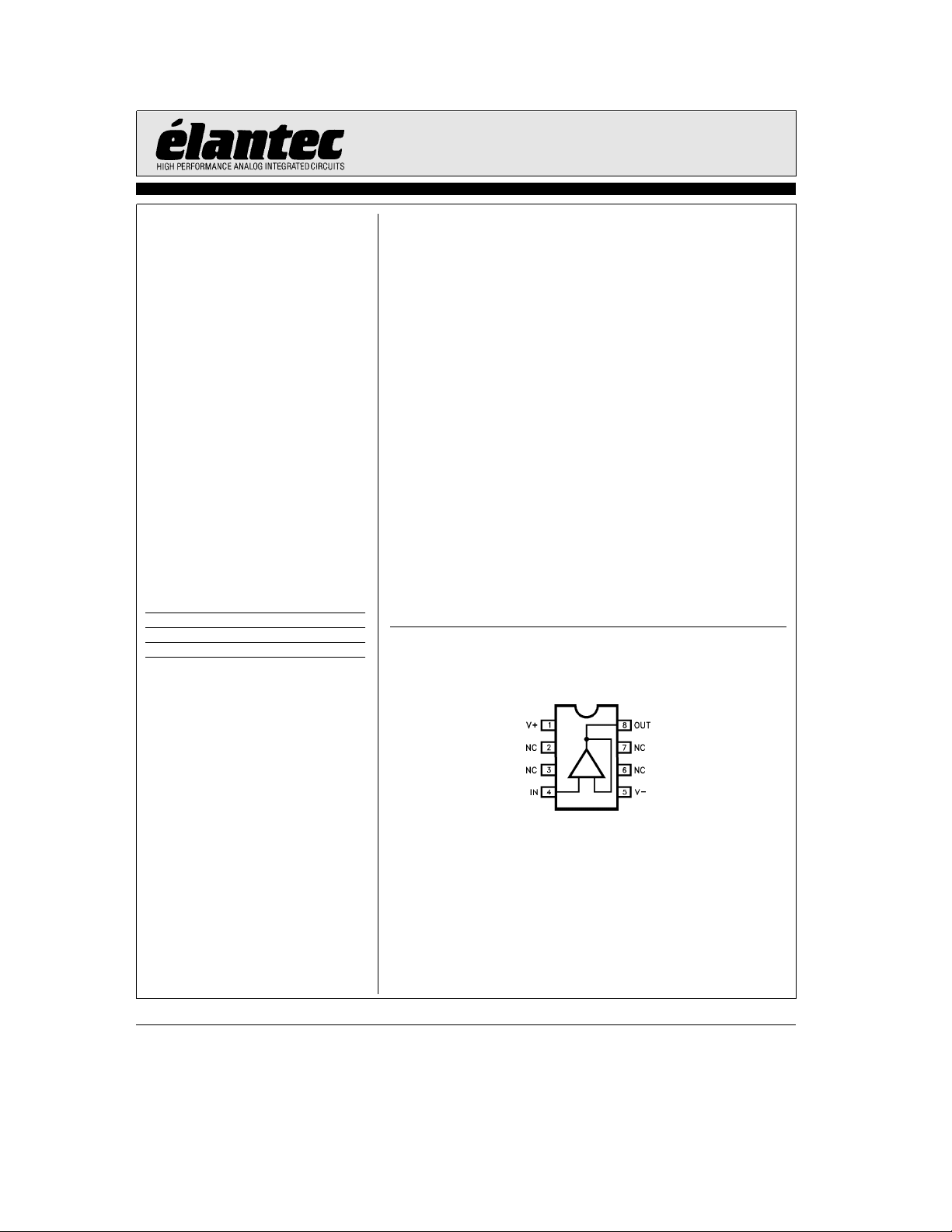
Connection Diagram
DIP and SO Package
Top View
Manufactured under U.S. Patent No. 4,893,091
Note: All information contained in this data sheet has been carefully checked and is believed to be accurate as of the date of publication; however, this data sheet cannot be a ‘‘controlled document’’. Current revisions, if any, to these
specifications are maintained at the factory and are available upon your request. We recommend checking the revision level before finalization of your design documentation.
©
1991 Elantec, Inc.
2072– 1
EL2072C
730 MHz Closed Loop Buffer
Absolute Maximum Ratings
Supply Voltage (V
Output Current Output is short-circuit protect-
Input Voltage
Important Note:
All parameters having Min/Max specifications are guaranteed. The Test Level column indicates the specific device testing actually
performed during production and Quality inspection. Elantec performs most electrical tests using modern high-speed automatic test
equipment, specifically the LTX77 Series system. Unless otherwise noted, all tests are pulsed tests, therefore T
Test Level Test Procedure
I 100% production tested and QA sample tested per QA test plan QCX0002.
II 100% production tested at T
III QA sample tested per QA test plan QCX0002.
IV Parameter is guaranteed (but not tested) by Design and Characterization Data.
V Parameter is typical value at T
)
S
ed to ground, however, maximum reliability is obtained if
does not exceed 70 mA.
I
OUT
T
MAX
and T
MIN
A
per QA test plan QCX0002.
e
(T
25§C)
A
g
7V
Operating Temperature
Junction Temperature 175
Storage Temperature
Thermal Resistance i
g
V
S
Note: See EL2071/EL2171 for Thermal Impedance curves.
e
25§C and QA sample tested at T
e
25§C for information purposes only.
A
b
40§Ctoa85§C
b
60§Ctoa150§C
e
95§C/W P-DIP
JA
e
175§C/W SO
i
JA
e
e
T
TA.
J
C
e
25§C,
A
§
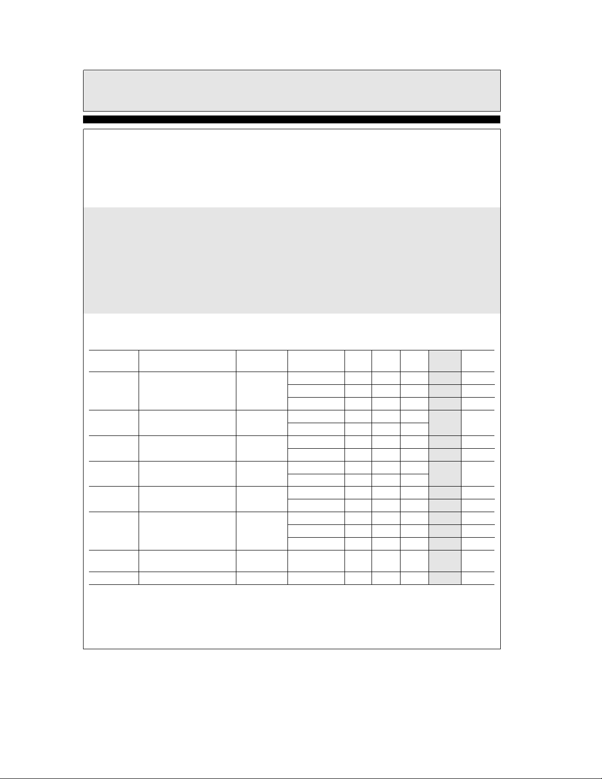
DC Electrical Characteristics
e
g
V
S
Parameter Description
V
OS
TCV
I
B
TCI
B
A
V
ILIN Integral End
PSRR Power Supply All 45.0 65.0 II dB
I
S
OS
5V, R
L
e
100X,R
e
50X unless otherwise specified
S
Test
Conditions Level
Temp Min Typ Max
Test
Output Offset Voltage 25§C 2.0 8.0 I mV
T
MIN
T
MAX
Average Offset 25§CbT
Voltage Drift
25
CbT
§
Input Bias Current 25§C, T
T
MIN
Average Input Bias 25§CbT
Current Drift
Small Signal Gain R
Point linearity
e
100X 25§C 0.96 0.98 I V/V
L
g
2V F.S. 25§C 0.2 0.4 IV %F.S.
25
CbT
§
T
MIN,TMAX
T
MIN
T
MAX
MAX
MIN
MAX
MAX
MIN
200.0 300.0
200.0 700.0
0.95 V V/V
16.0 V mV
13.0 V mV
20.0 50.0
IV mV/
20.0 100.0
10.0 50.0 II mA
100.0 V mA
IV nA/
0.8 IV %F.S.
0.3 IV %F.S.
Rejection Ratio
Supply CurrentÐQuiescent No Load All 15.0 20.0 II mA
Units
C
§
C
§
C
TDis 3.3in
2
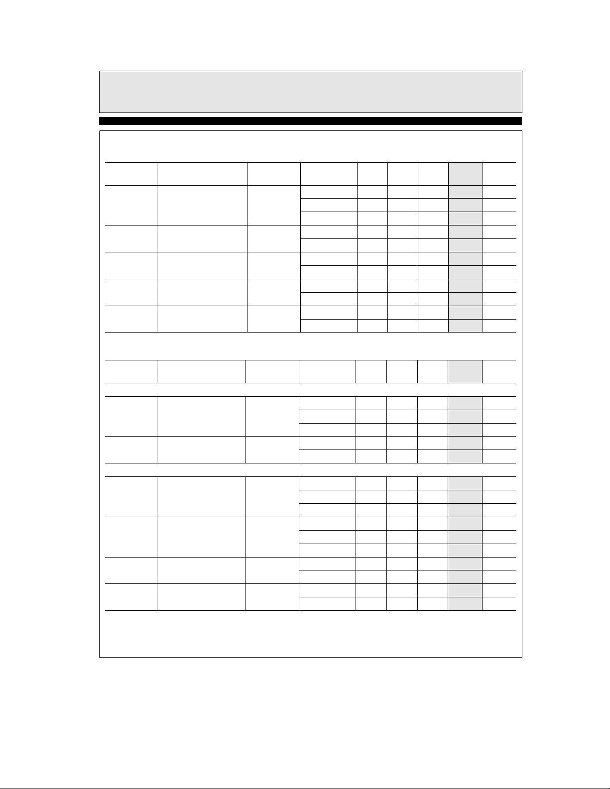
DC Electrical Characteristics
e
g
V
S
Parameter Description
R
IN
C
IN
R
OUT
I
OUT
V
OUT
5V, R
L
e
100X,R
e
50X unless otherwise specified Ð Contd.
S
Conditions Level
Input Resistance 25§C 100.0 160.0 I kX
Input Capacitance 25§C 1.6 2.2 IV pF
Output Impedance (DC) 25§C 2.0 3.0 IV X
Output Current 25§C, T
Output Voltage Swing R
Test
e
100X 25§C, T
L
EL2072C
730 MHz Closed Loop Buffer
Temp Min Typ Max
T
MIN
T
MAX
T
MIN,TMAX
T
MIN,TMAX
T
MIN
T
MIN
MAX
MAX
50.0 V kX
200.0 V kX
2.5 IV pF
3.5 IV X
50.0 70.0 II mA
45.0 V mA
g
g
g
3.2
4.0 II V
3.0 V V
Test
Units
TDis 2.4inTDis 3.5in
AC Electrical Characteristics
Parameter Description
FREQUENCY RESPONSE
SSBW
LSBW
b
3 dB Bandwidth 25§C 400.0 730.0 V MHz
k
(V
b
(V
0.5 VPP)
OUT
3 dB Bandwidth 25§C 55.0 90.0 IV MHz
e
5.0 VPP)
OUT
GAIN FLATNESS
GFPL Peaking
k
V
0.5 V
OUT
PP
GFR Rolloff
k
V
0.5 V
OUT
PP
GDL Group Delay
LPD Linear Phase Deviation
k
V
0.5 V
OUT
PP
Conditions Level
k
k
k
k
Test
e
V
S
g
5V, R
L
e
100X,R
e
50X unless otherwise specified
S
Temp Min Typ Max
T
MIN
T
MAX
T
MIN,TMAX
400.0 IV MHz
300.0 IV MHz
50.0 IV MHz
Test
Units
200 MHz 25§C 0.0 0.5 V dB
T
T
MAX
MIN
0.6 IV dB
0.8 IV dB
200 MHz 25§C 0.0 0.8 V dB
T
MIN
T
MAX
200 MHz 25§C, T
T
MAX
200 MHz 25
§
T
C, T
MAX
MIN
MIN
0.75 1.0 IV ns
0.7 1.5 IV
1.0 IV dB
1.2 IV dB
1.2 IV ns
2.0 IV
§
§
3

EL2072C
730 MHz Closed Loop Buffer
AC Electrical Characteristics
e
g
V
S
Parameter Description
5V, R
L
e
100X,R
e
50X unless otherwise specified
S
Ð Contd.
Test
Conditions Level
Temp Min Typ Max
Test
Units
TIME-DOMAIN RESPONSE
TR1, TF1 Rise Time, Fall Time 0.5V Step 25§C, T
Input Signal Rise/Falle300 ps
T
MAX
MIN
0.4 1.0 IV ns
1.4 IV ns
TR2, TF2 Rise Time, Fall Time 5.0V Step 25§C 4.5 7.5 IV ns
Input Signal Rise/Falls1ns T
TS1 Settling Time to 0.2% 2.0V Step
Input Signal Rise/Falls1ns
MIN,TMAX
All 5.0 10.0 IV ns
8.5 IV ns
OS Overshoot 0.5V Step 25§C 0.0 10.0 IV %
Input Signal Rise/Falle300 ps
T
MIN,TMAX
15.0 IV %
SR Slew Rate 25§C 500.0 800.0 IV V/ms
T
MIN,TMAX
450.0 IV V/ms
DISTORTION
HD2 2nd Harmonic Distortion 2 V
at 20 MHz
HD2A 2nd Harmonic Distortion 2 V
at 50 MHz
HD3 3rd Harmonic Distortion 2 V
at 20 MHz
HD3A 3rd Harmonic Distortion 2 V
at 50 MHz
PP
PP
PP
PP
25§C
T
MIN
T
MAX
25§C,T
T
MIN
25§C
T
MIN,TMAX
25§C,T
T
MAX
MAX
MIN
b
55.0b50.0 V dBc
b
48.0 IV dBc
b
55.0 IV dBc
b
50.0b45.0 IV dBc
b
40.0 IV dBc
b
65.0b55.0 V dBc
b
55.0 IV dBc
b
60.0b50.0 IV dBc
b
45.0 IV dBc
EQUIVALENT INPUT NOISE
NF Noise Floor 25§C, T
l
100 kHz
T
MAX
INV Integrated Noise 25§C, T
100 kHz to 200 MHz
T
MAX
MIN
MIN
b
158.0b155.0 IV dBm (1 Hz)
b
154.0 IV dBm (1 Hz)
40.0 57.0 IV mV
63.0 IV mV
TDis 5.1in
4

EL2072C
730 MHz Closed Loop Buffer
Typical Performance Curves
Forward Gain and Phase from Linear Phase
Input Impedance Output Impedance Load Capacitance
e
g
(V
S
Gain Flatness & Deviation
5V, R
L
e
100X,R
e
50X)
S
Reverse Gain and phase
Recommended R
vs
S
Integral Linearity Error Frequency Response vs R
5
load
S
vs C
l
l
21
load
with Recommended R
s
2072– 2

EL2072C
730 MHz Closed Loop Buffer
Typical Performance Curves
Small Signal
Pulse Response
2nd Harmonic Distortion 3rd Harmonic Distortion Intermodulation Intercept
e
g
(V
5V, R
S
Large Signal
Pulse Response
L
e
100X,R
e
50X) Ð Contd.
S
Long-Term
Settling Time
2-Tone, 3rd Order
2072– 3
6

Burn-In Circuit
EL2072C
730 MHz Closed Loop Buffer
2072– 4
Printed Circuit Layout
As with any high-frequency device, good PCB
layout is necessary for optimum performance.
This is especially important for the EL2072,
which has a typical bandwidth of 730 MHz.
Ground plane construction is a requirement, as is
good power-supply bypassing close to the package. A closely-placed 0.01 mF ceramic capacitor
between each supply pin and the ground plane is
usually sufficient decoupling.
Pins 2, 3, 6, and 7 should be connected to the
ground-plane to minimize capacitive feedthrough, and all input and output traces should
be laid out as transmission lines and terminated
as close to the EL2072 package as possible.
Increasing capacitance on the output of the
EL2072 will add phase shift, decreasing phase
margin and increasing frequency-response peaking. A small series resistor before the capacitance
decouples this effect, and should be used for large
capacitance values. Please refer to the graphs for
the appropriate resistor value to be used.
7

EL2072C
730 MHz Closed Loop Buffer
EL2072CDecember 1995 Rev E
General Disclaimer
Specifications contained in this data sheet are in effect as of the publication date shown. Elantec, Inc. reserves the right to make changes
in the circuitry or specifications contained herein at any time without notice. Elantec, Inc. assumes no responsibility for the use of any
circuits described herein and makes no representations that they are free from patent infringement.
WARNING Ð Life Support Policy
Elantec, Inc. products are not authorized for and should not be
used within Life Support Systems without the specific written
consent of Elantec, Inc. Life Support systems are equipment in-
Elantec, Inc.
1996 Tarob Court
Milpitas, CA 95035
Telephone: (408) 945-1323
(800) 333-6314
Fax: (408) 945-9305
European Office: 44-71-482-4596
tended to support or sustain life and whose failure to perform
when properly used in accordance with instructions provided can
be reasonably expected to result in significant personal injury or
death. Users contemplating application of Elantec, Inc. products
in Life Support Systems are requested to contact Elantec, Inc.
factory headquarters to establish suitable terms & conditions for
these applications. Elantec, Inc.’s warranty is limited to replacement of defective components and does not cover injury to persons or property or other consequential damages.
Printed in U.S.A.8
 Loading...