

Page 1
EL2020C
50 MHz Current Feedback Amplifier
EL2020C December 1995 Rev G
Features
# Slew rate 500 V/ ms
g
#
33 mA output current
# Drives
# Differential phase
g
2.4V into 75X
k
0.1
§
# Differential gaink0.1%
# V supply
g
5V tog18V
# Output short circuit protected
# Uses current mode feedback
# 1% settling time of 50 ns for 10V
step
# Low cost
# 9 mA supply current
# 8-pin mini-dip
Applications
# Video gain block
# Residue amplifier
# Radar systems
# Current to voltage converter
# Coax cable driver with
gain of 2
Ordering Information
Part No. Temp. Range Pkg. Outline
EL2020CNb40§Ctoa85§C P-DIP MDP0031
EL2020CMb40§Ctoa85§C 20-Lead MDP0027
SOL
General Description
The EL2020 is a fast settling, wide bandwidth amplifier optimized for gains between
monolithic Complementary Bipolar process, this amplifier uses
current mode feedback to achieve more bandwidth at a given
gain then a conventional voltage feedback operational amplifier.
The EL2020 will drive two double terminated 75X coax cables
to video levels with low distortion. Since it is a closed loop device, the EL2020 provides better gain accuracy and lower distortion than an open loop buffer. The device includes output short
circuit protection, and input offset adjust capability.
The bandwidth and slew rate of the EL2020 are relatively independent of the closed loop gain taken. The 50 MHz bandwidth
at unity gain only reduces to 30 MHz at a gain of 10. The
EL2020 may be used in most applications where a conventional
op amp is used, with a big improvement in speed power product.
Elantec products and facilities comply with Elantec document,
QRA-1: Processing-Monolithic Products.
b
10 anda10. Built using the Elantec
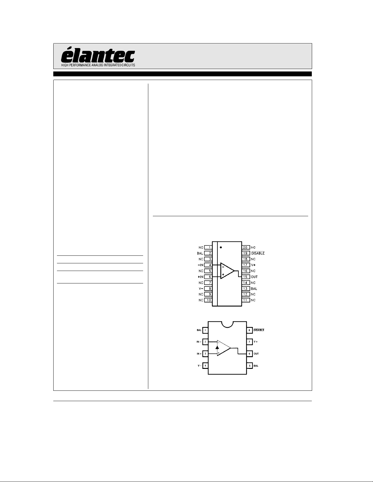
Connection Diagrams
SOL
Ý
2020– 2
DIP
2020– 1
Manufactured under U.S. Patent No. 4,893,091.
Note: All information contained in this data sheet has been carefully checked and is believed to be accurate as of the date of publication; however, this data sheet cannot be a ‘‘controlled document’’. Current revisions, if any, to these
specifications are maintained at the factory and are available upon your request. We recommend checking the revision level before finalization of your design documentation.
©
1989 Elantec, Inc.
Page 2
EL2020C
50 MHz Current Feedback Amplifier
Absolute Maximum Ratings
V
V
DV
I
I
P
I
S
IN
IN
INS
D
OP
Supply Voltage
Input Voltage
Differential Input Voltage
IN
Input Current (Pins 2 or 3)
Input Current (Pins 1, 5, or 8)
Maximum Power Dissipation
(See Curves) 1.25W
Peak Output Current Short Circuit
(25§C)
g
18V or 36V
g
15V or V
g
g
Protected
g
10V
10 mA
5mA
T
Operating Temperature Range
A
T
S
Operating Junction Temperature
J
T
Plastic Package, SOL 150
Storage Temperature
ST
b
40§Ctoa85§C
b
65§Ctoa150§C
C
§
Output Short Circuit Duration
(Note 2) Continuous
Important Note:
All parameters having Min/Max specifications are guaranteed. The Test Level column indicates the specific device testing actually
performed during production and Quality inspection. Elantec performs most electrical tests using modern high-speed automatic test
equipment, specifically the LTX77 Series system. Unless otherwise noted, all tests are pulsed tests, therefore T
Test Level Test Procedure
I 100% production tested and QA sample tested per QA test plan QCX0002.
II 100% production tested at T
III QA sample tested per QA test plan QCX0002.
IV Parameter is guaranteed (but not tested) by Design and Characterization Data.
V Parameter is typical value at T
T
MAX
and T
per QA test plan QCX0002.
MIN
Open Loop Characteristics
Parameter Description Temp
VOS(Note 1) Input Offset Voltage 25§C
DVOS/DT Offset Voltage Drift
e
25§C and QA sample tested at T
A
e
25§C for information purposes only.
A
e
g
V
15V
S
T
MIN,TMAX
e
25§C,
A
Limits
Min Typ Max
b
10 3
b
15
a
a
b
30 V mV/§C
10 I mV
15 III mV
e
e
T
TA.
J
C
Test Level Units
CMRR (Note 3) Common Mode Rejection Ratio ALL 50 60 II dB
PSRR (Note 4) Power Supply Rejection Ratio 25§C6575 I dB
T
a
I
IN
a
R
IN
a
IPSR (Note 4) Non-Inverting Input Current 25§C, T
Non-inverting Input Current 25§C, T
Non-Inverting Input Resistance ALL 1 5 II MX
Power Supply Rejection
b
IIN(Note 1)
b
Input Current 25§C, T
MIN,TMAX
MAX
T
MIN
MAX
T
MIN
MAX
T
MIN
60 III dB
b
15 5
b
25
a
15 II mA
a
25 III mA
0.05 0.5 II mA/V
1.0 III mA/V
b
40 10
b
50
a
40 II mA
a
50 III mA
TDis 2.8in
2
Page 3

50 MHz Current Feedback Amplifier
e
Open Loop Characteristics
Parameter Description Temp
b
ICMR (Note 3)bInput Current 25§C, T
b
IPSR (Note 4)
R
ol
A
VOL1
A
VOL2
V
O
I
OUT
I
s
I
s off
I
logic
I
D
I
e
Common Mode Rejection
b
Input Current 25§C, T
Power Supply Rejection
Transimpedence (DV
e
R
400X,V
L
OUT
e
OUT
g
Open Loop DC Voltage Gain 25§C, T
e
R
400X,V
L
OUT
e
g
Open Loop DC Voltage Gain 25§C, T
e
R
100X,V
L
OUT
e
g
Output Voltage Swing 25§C, T
e
R
400X
L
Output Current 25§C, T
e
R
400X
L
Quiescent Supply Current 25§C 9 12 I mA
Supply Current, Disabled, V
Pin 8 Current, Pin 8e0V ALL 1.1 1.5 II mA
Min Pin 8 Current to Disable ALL 120 250 II mA
Max Pin 8 Current to Enable ALL 30 II mA
g
V
15V Ð Contd.
S
/D(bIIN)) 25§C, T
10V
10V
2.5V
e
0V ALL 5.5 7.5 II mA
8
MAX
T
MIN
MAX
T
MIN
MAX
T
MIN
MAX
T
MIN
MAX
T
MIN
MAX
T
MIN
MAX
T
MIN
T
MIN,TMAX
EL2020C
Limits
Min Typ Max
0.5 2.0 II mA/V
0.05 0.5 II mA/V
300 1000 II V/mA
50 III V/mA
70 80 II dB
60 III dB
60 70 II dB
55 III dB
g
g
g
g
g
12
13 II V
11 III V
g
30
32.5 II mA
27.5 III mA
Test Level Units
4.0 III mA/V
1.0 III mA/V
15 III mA
TDis 4.1in
3
Page 4

EL2020C
50 MHz Current Feedback Amplifier
e
AC Closed Loop Characteristics EL2020C
g
V
S
Parameter Description Min Typ Max
Closed Loop Gain of 1 V/V (0 dB), R
SR1 Slew Rate, R
FPBW1 Full Power Bandwidth (Note 5) 4.77 7.95 I MHz
t
1 Rise Time, R
r
t
1 Fall Time, R
f
tp1 Propagation Delay, R
l
l
e
l
e
400X,V
e
100X,V
100X,V
e
l
e
O
OUT
OUT
100X,V
Closed Loop Gain of 1 V/V (0 dB), R
BW
t
s
t
s
b
3 dB Small Signal Bandwidth, R
1% Settling Time, R
0.1% Settling Time, R
e
l
l
400X,V
e
400X,V
Closed Loop Gain of 10 V/V (20 dB), R
SR10 Slew Rate, R
FPBW10 Full Power Bandwidth (Note 5) 4.77 7.95 I MHz
t
10 Rise Time, R
r
t
10 Fall Time, R
f
t
10 Propagation Delay, R
p
e
l
l
e
l
400X,V
e
100X,V
100X,V
e
l
e
O
OUT
OUT
100X,V
Closed Loop Gain of 10 V/V (20 dB), R
BW
t
s
t
s
Note 1: The offset voltage and inverting input current can be adjusted with an external 10 kX pot between pins 1 and 5 with the
wiper connected to V
Note 2: A heat sink is required to keep the junction temperature below the absolute maximum when the output is short circuited.
Note 3: V
g
Note 4:
Note 5: Full Power Bandwidth is guaranteed based on Slew Rate measurement. FPBW
b
1% Settling Time, R
0.1% Settling Time, R
e
g
10V.
CM
4.5VsV
S
3 dB Small Signal Bandwidth, R
e
400 X,V
l
e
400X,V
l
(Pin 7) to make the output offset voltage zero.
CC
s
g
18V.
e
1kX
F
g
10V, test at V
e
1V, 10% to 90% 6 V ns
e
1V, 10% to 90% 6 V ns
OUT
F
e
l
e
10V 50 V ns
O
e
O
g
10V, Test at V
e
1V, 10% to 90% 25 V ns
e
1V, 10% to 90% 25 V ns
OUT
e
l
e
O
e
O
e
g
5V 300 500 I V/ms
O
e
1V, 50% Points 8 V ns
e
820X
100X,V
e
100 mV 50 V MHz
O
10V 90 V ns
e
1kX,R
F
e
1V, 50% points 12 V ns
e
680X,R
F
100X,V
10V 55 V ns
e
111X
G
e
g
5V 300 500 I V/ms
O
e
76X
G
e
100 mV 30 V MHz
O
10V 280 V ns
15V, T
e
e
25§C
A
SR/2qV
peak
Test
Level
Units
.
TDis 3.2in
4
Page 5
EL2020C
50 MHz Current Feedback Amplifier
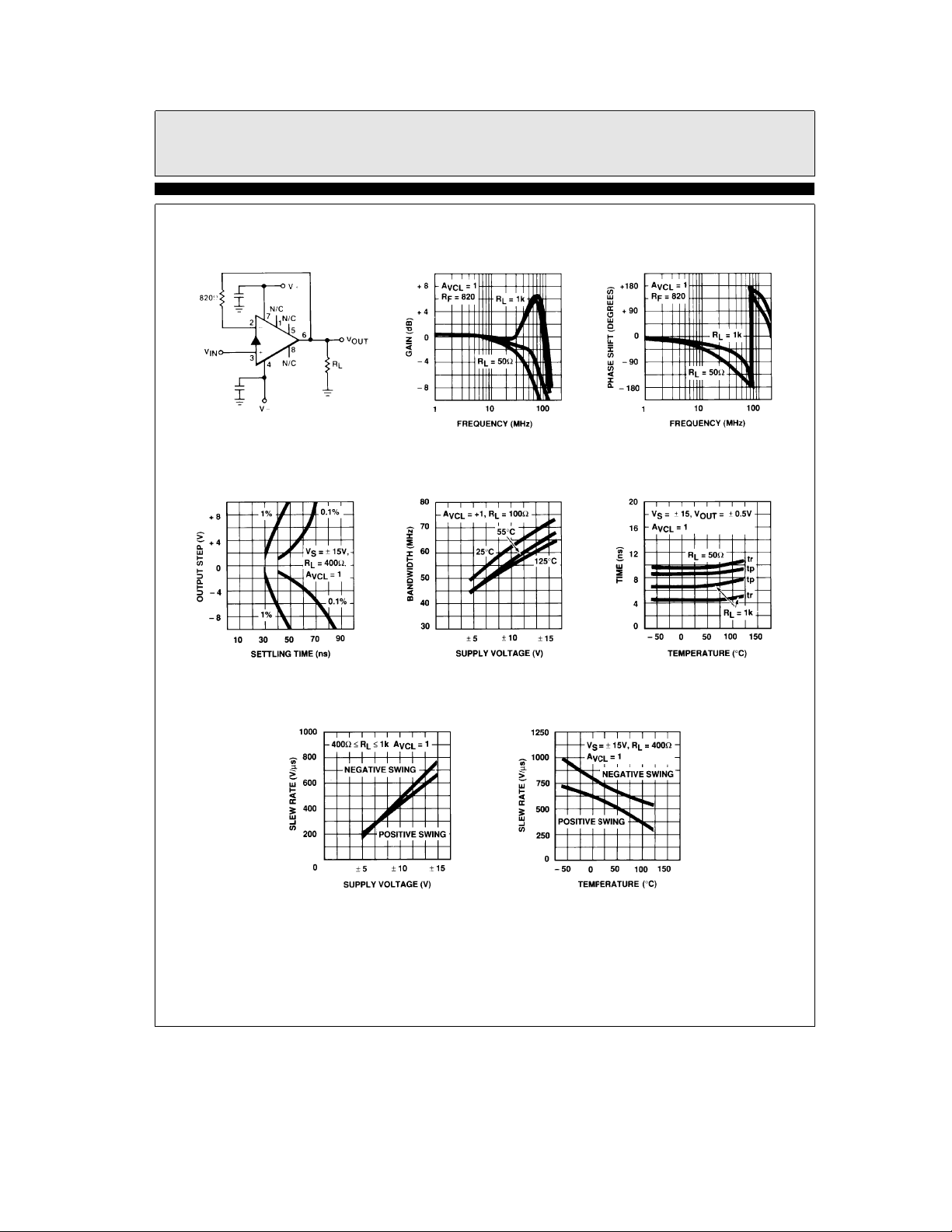
Typical Performance Curves
ea
A
1 Gain vs Frequency Frequency
VCL
Settling Time vs
Output Swing
Non-Inverting Gain of One
b
3 dB Bandwidth vs
Supply Voltage
Phase Shift vs
Rise Time and
Prop Delay vs
Temperature
Slew Rate vs
Supply Voltage
Slew Rate vs
Temperature
2020– 4
5
Page 6
EL2020C
50 MHz Current Feedback Amplifier
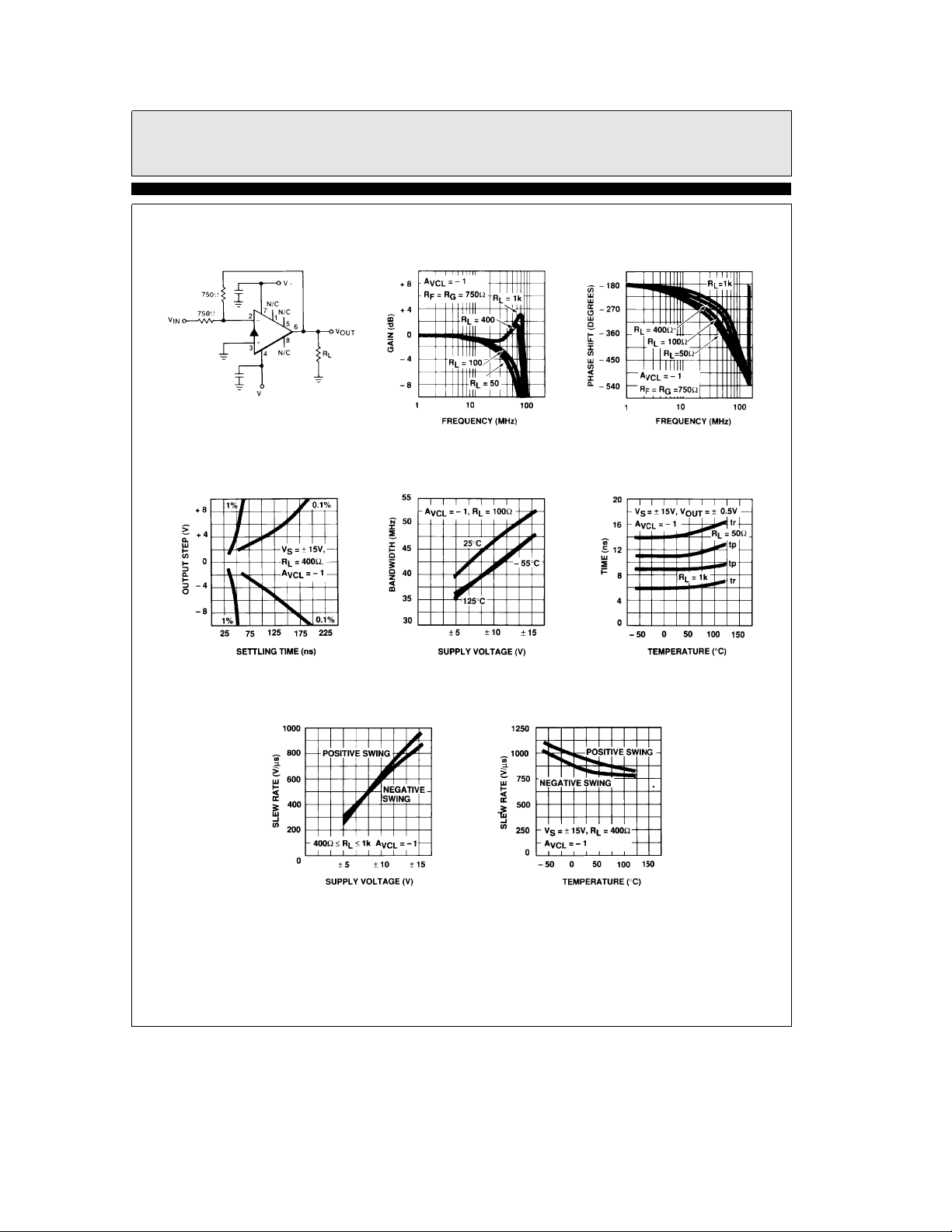
Typical Performance Curves
eb
A
Settling Time vs
Output Swing
1 Gain vs Frequency Frequency
VCL
Ð Contd. Inverting Gain of One
b
3 dB Bandwidth vs
Supply Voltage
Phase Shift vs
Rise Time and
Prop Delay vs
Temperature
Slew Rate vs
Supply Voltage
Slew Rate vs
Temperature
2020– 5
6
Page 7

EL2020C
50 MHz Current Feedback Amplifier
Typical Performance Curves
ea
A
Settling Time vs
Output Swing
2 Gain vs Frequency Frequency
VCL
Ð Contd. Non-Inverting Gain of Two
b
3 dB Bandwidth vs
Supply Voltage
Phase Shift vs
Rise Time and
Prop Delay vs
Temperature
Slew Rate vs
Supply Voltage
Slew Rate vs
Temperature
2020– 6
7
Page 8

EL2020C
50 MHz Current Feedback Amplifier
Typical Performance Curves
ea
A
Settling Time vs
Output Swing
10 Gain vs Frequency Frequency
VCL
Ð Contd. Non-Inverting Gain of Ten
b
3 dB Bandwidth vs
Supply Voltage
Phase Shift vs
Rise Time and
Prop Delay vs
Temperature
Slew Rate vs
Supply Voltage
Slew Rate vs
Temperature
2020– 7
8
Page 9

EL2020C
50 MHz Current Feedback Amplifier
Typical Performance Curves
Maximum Undistorted
Output Voltage vs
Frequency
Voltage Noise vs
Frequency
Ð Contd.
Input Resistance vs
Temperature
Current Noise vs
Frequency
PSRR vs Frequency
Output Impedance vs
Frequency
Supply Current vs
Supply Voltage
8-Lead Plastic DIP
Maximum Power Dissipation
vs Ambient Temperature
9
20-Lead SOL
Maximum Power Dissipation
vs Ambient Temperature
2020– 8
Page 10

EL2020C
50 MHz Current Feedback Amplifier
Application Information
Theory of Operation
The EL2020 has a unity gain buffer similar to the
EL2003 from the non-inverting input to the inverting input. The error signal of the EL2020 is a
current flowing into (or out of) the inverting input. A very small change in current flowing
through the inverting input will cause a large
change in the output voltage. This current amplification is the transresistance (R
EL2020[V
very large (&10
e
OUT
ROL* I
6
), the current flowing into the
INV
inverting input in the steady state (non-slewing)
condition is very small.
Therefore we can still use op-amp assumptions as
a first order approximation for circuit analysis,
namely that. . .
1. The voltage across the inputs&0 and
2. The current into the inputs is&0
Simplified Block Diagram of EL2020
)ofthe
OL
]
. Since R
OL
in a lower
frequency is limited by a zero in the closed loop
transfer function which results from stray capacitance between the inverting input and ground.
Power Supplies
The EL2020 may be operated with single or split
power supplies as low as
high as
significantly for supply voltages less than
(10V total), but the bandwidth only changes 25%
for supplies from
is
sary to use equal value split power supplies, i.e.,
b
video signals. Bypass capacitors from each supply pin to a ground plane are recommended. The
EL2020 will not oscillate even with minimal bypassing, however, the supply will ring excessively
with inadequate capacitance. To eliminate supply
ringing and the errors it might cause, a 4.7 mF
tantalum capacitor with short leads is recommended for both supplies. Inadequate supply bypassing can also result in lower slew rate and
longer settling times.
b
3 dB frequency. Attenuation at high
g
g
18V (36V total). The slew rate degrades
g
3V tog18V. It is not neces-
3V (6V total) to as
g
5V
5V anda12V would be excellent for 0V to 1V
Non-Inverting Amplifier
2020– 10
Resistor Value Selection and
Optimization
The value of the feedback resistor (and an internal capacitor) sets the AC dynamics of the
EL2020. A nominal value for the feedback resistor is 1 kX, which is the value used for production testing. This value guarantees stability. For
a given gain, the bandwidth may be increased by
decreasing the feedback resistor and, conversely,
the bandwidth will be decreased by increasing
the feedback resistor.
Reducing the feedback resistor too much will result in overshoot and ringing, and eventually oscillations. Increasing the feedback resistor results
EL2020 Typical Non-Inverting
Amplifier Characteristics
A
R
V
a
1 820X None 50 MHz 50 ns 90 ns
a
2 750X 750X 50 MHz 50 ns 100 ns
a
5 680X 170X 50 MHz 50 ns 200 ns
a
10 680X 76X 30 MHz 55 ns 280 ns
10
RGBandwidth Settling Time
F
2020– 11
10V
1% 0.1%
Page 11

EL2020C
50 MHz Current Feedback Amplifier
Application Information
Summing Amplifier
EL2020 Typical Inverting
Amplifier Characteristics
A
RFR1,R2Bandwidth Settling Time
V
b
1 750X 750X 40 MHz 50 ns 130 ns
b
2 750X 375X 40 MHz 55 ns 160 ns
b
5 680X 130X 40 MHz 55 ns 160 ns
b
10 680X 68X 30 MHz 70 ns 170 ns
Ð Contd.
2020– 12
10V
1% 0.1%
Input Range
The non-inverting input to the EL2020 looks like
a high resistance in parallel with a few picofarads
in addition to a DC bias current. The input characteristics change very little with output loading,
even when the amplifier is in current limit.
pling. Inductive sources may cause oscillations; a
1kXresistor in series with the input lead will
usually eliminate problems without sacrificing
too much speed.
Current Limit
The EL2020 has internal current limits that protect the output transistors. The current limit
goes down with junction temperature rise. At a
junction temperature of
a
175§C the current limits are at about 50 mA. If the EL2020 output is
shorted to ground when operating on
g
15V sup-
plies, the power dissipation could be as great as
1.1W. A heat sink is required in order for the
EL2020 to survive an indefinite short. Recovery
time to come out of current limit is about 50 ns.
Using the 2020 with Output Buffers
When more output current is required, a wideband buffer amplifier can be included in the feedback loop of the EL2020. With the EL2003 the
subsystem overshoots about 10% due to the
phase lag of the EL2003. With the EL2004 in the
loop, the overshoot is less than 2%. For even
more output current, several buffers can be paralleled.
EL2020 Buffered with an EL2004
The input charactersitics also change when the
input voltage exceeds either supply by 0.5V. This
happens because the input transistor’s base-collector junctions forward bias. If the input exceeds
the supply by LESS than 0.5V and then returns
to the normal input range, the output will recover in less than 10 ns. However if the input exceeds the supply by MORE than 0.5V, the recovery time can be 100’s of nanoseconds. For this
reason it is recommended that Schottky diode
clamps from input to supply be used if a fast recovery from large input overloads is required.
Source Impedance
The EL2020 is fairly tolerant of variations in
source impedances. Capacitive sources cause no
problems at all, resistive sources up to 100 kX
present no problems as long as care is used in
board layout to minimize output to input cou-
2020– 13
Capacitive Loads
The EL2020 is like most high speed feedback amplifiers in that it does not like capacitive loads
between 50 pF and 1000 pF. The output resistance works with the capacitive load to form a
second non-dominate pole in the loop. This results in excessive peaking and overshoot and can
lead to oscillations. Standard resistive isolation
techniques used with other op amps work well to
isolate capacitive loads from the EL2020.
11
Page 12

EL2020C
50 MHz Current Feedback Amplifier
Application Information
Ð Contd.
Offset Adjust
To calculate the amplifier system offset voltage
from input to output we use the equation:
Output Offset Voltage
I
BIAS(RF
The EL2020 output offset can be nulled by using
a10kXpotentiometer from pins 1 to 5 with the
slider tied to pin 7 (
offset voltage and the inverting input bias current. The typical adjustment range is
the output.
)
e
VOS(RF/R
a
VCC). This adjusts both the
a
G
g
80 mV at
g
1)
Compensation
The EL2020 is internally compensated to work
with external feedback resistors for optimum
bandwidth over a wide range of closed loop gain.
The part is designed for a nominal 1 kX of feedback resistance, although it is possible to get
more bandwidth by decreasing the feedback resistance.
The EL2020 becomes less stable by adding capacitance in parallel with the feedback resistor,
so feedback capacitance is not recommended.
The EL2020 is also sensitive to stray capacitance
from the inverting input to ground, so the board
should be laid out to keep the physical size of this
node small, with ground plane kept away from
this node.
Active Filters
The EL2020’s low phase lag at high frequencies
makes it an excellent choice for high performance
active filters. The filter response more closely approaches the theoritical response than with conventional op amps due to the EL2020’s smaller
propagation delay. Because the internal compensation of the EL2020 depends on resistive feedback, the EL2020 should be set up as a gain
block.
Driving Cables
The EL2020 was designed with driving coaxial
cables in mind. With 30 mA of output drive and
low output impedance, driving one to three 75X
double terminated coax cables with one EL2020
is practical. Since it is easy to set up a gain of
a
2, the double matched method is the best way
to drive coax cables, because the impedance
match on both ends of the cable will suppress
reflections. For a discussion on some of the other
ways to drive cables, see the section on driving
cables in the EL2003 data sheet.
Video Performance Characteristics
The EL2020 makes an excellent gain block for
video systems, both RS-170 (NTSC) and faster.
It is capable of driving 3 double terminated 75X
cables with distortion levels acceptable to broadcasters. A common video application is to drive a
75X double terminated coax with a gain of 2.
To measure the video performance of the EL2020
in the non-inverting gain of 2 configuration, 5
identical gain-of-two circuits were cascaded (with
a divide by two 75X attenuator between each
stage) to increase the errors.
The results, shown in the photos, indicate the entire system of 5 gain-of-two stages has a differential gain of 0.5% and a differential phase of 0.5
This implies each device has a differential
gain/phase of 0.1% and 0.1
small to measure on single devices.
Differential Phase Differential Gain
of 5 Cascaded of 5 Cascaded
Gain-Of-Two Stages Gain-Of-Two Stages
, but these are too
§
.
§
2020– 14
12
Page 13

EL2020C
50 MHz Current Feedback Amplifier
Application Information
Ð Contd.
Video Distribution Amplifier
The distribution amplifier shown below features
a difference input to reject common mode signals
on the 75X coax cable input. Common mode rejection is often necessary to help to eliminate
60 Hz noise found in production environments.
Video Distribution Amplifier
with Difference Input
2020– 15
EL2020 Disable/Enable Operation
The EL2020 has an enable/disable control input
at pin 8. The device is enabled and operates normally when pin 8 is left open or returned to pin 7,
V
. When more than 250 mA is pulled from pin
CC
8, the EL2020 is disabled. The output becomes a
high impedance, the inverting input is no longer
driven to the positive input voltage, and the supply current is halved. To make it easy to use this
feature, there is an internal resistor to limit the
current to a safe level (E1.1 mA) if pin 8 is
grounded.
Using the EL2020 as a Multiplexer
An interesting use of the enable feature is to combine several amplifiers in parallel with their outputs common. This combination then acts similar to a MUX in front of an amplifier. A typical
circuit is shown.
When the EL2020 is disabled, the DC output impedance is very high, over 10 kX. However there
is also an output capacitance that is non-linear.
For signals of less than 5V peak to peak, the output capacitance looks like a simple 15 pF capacitor. However, for larger signals the output capacitance becomes much larger and non-linear.
The example multiplexer will switch between
amplifiers in 5 ms for signals of less than
the outputs. For full output signals of 20V peak
to peak, the selection time becomes 25 ms. The
disabled outputs also present a capacitive load
and therefore only three amplifiers can have their
outputs shorted together. However an unlimited
number can sum together if a small resistor
(25X) is inserted in series with each output to
isolate it from the ‘‘bus’’. There will be a small
gain loss due to the resistors of course.
Using the EL2020 as a Multiplexer
g
2V on
To draw current out of pin 8 an ‘‘open collector
output’’ logic gate or a discrete NPN transistor
can be used. This logic interface method has the
advantage of level shifting the logic signal from
5V supplies to whatever supply the EL2020 is operating on without any additional components.
2020– 16
13
Page 14

EL2020C
50 MHz Current Feedback Amplifier
Burn-In Circuit
Equivalent Circuit
Pin numbers are for DIP Packages.
2020– 17
All Packages Use the Same Schematic.
2020– 18
14
Page 15

EL2020C
50 MHz Current Feedback Amplifier
EL2020 Macromodel
* Revision A. March 1992
* Enhancements include PSRR, CMRR, and Slew Rate Limiting
* Connections:
*
*
*
*
*
.subckt M2020 3 2746
*
*Input Stage
*
e1100301.0
vis 10 9 0V
h2 9 12 vxx 1.0
r121150
l1 11 12 29nH
iinp3010mA
iinm205mA
*
*Slew Rate Limiting
*
h1 13 0 vis 600
r2 13 14 1K
d1 14 0 dclamp
d2 0 14 dclamp
*
* High Frequency Pole
*
*e2 30 0 14 0 0.00166666666
15 30 17 1.5mH
c5 17 0 1pF
r5 17 0 500
*
* Transimpedance Stage
*
g10181701.0
rol 18 0 1Meg
cdp 18 0 5pF
*
* Output Stage
*
q141819qp
q271820qn
q371921qn
q442022qp
r7 21 6 4
r8 22 6 4
a
input
b
input
l
ll
lll
llll
a
Vsupply
b
Vsupply
output
lllll
TABWIDE
TDis 6.4in
15
Page 16

EL2020C
50 MHz Current Feedback Amplifier
EL2020 Macromodel
ios1 7 19 2.5mA
ios2 20 4 2.5mA
*
* Supply
*
ips 7 4 3mA
*
* Error Terms
*
ivos 0 23 5mA
vxx 23 0 0V
e4240601.0
e5250701.0
e6260401.0
r9 24 23 1K
r10 25 23 1K
r11 26 23 1K
*
* Models
*
.model qn npn (is
.model qp pnp (is
.model dclamp d(is
.ends
e5eb
15 bfe100 tfe0.2nS)
e5eb
15 bfe100 tfe0.2nS)
e1eb
30 ibve0.266 bve1.67 ne4)
Ð Contd.
TDis 3.1in
16
Page 17

EL2020 Macromodel
EL2020C
50 MHz Current Feedback Amplifier
2020– 22
17
Page 18

BLANK
18
Page 19

BLANK
19
Page 20

EL2020C
50 MHz Current Feedback Amplifier
EL2020CDecember 1995 Rev G
General Disclaimer
Specifications contained in this data sheet are in effect as of the publication date shown. Elantec, Inc. reserves the right to make changes
in the circuitry or specifications contained herein at any time without notice. Elantec, Inc. assumes no responsibility for the use of any
circuits described herein and makes no representations that they are free from patent infringement.
WARNING Ð Life Support Policy
Elantec, Inc. products are not authorized for and should not be
used within Life Support Systems without the specific written
consent of Elantec, Inc. Life Support systems are equipment in-
Elantec, Inc.
1996 Tarob Court
Milpitas, CA 95035
Telephone: (408) 945-1323
(800) 333-6314
Fax: (408) 945-9305
European Office: 44-71-482-4596
tended to support or sustain life and whose failure to perform
when properly used in accordance with instructions provided can
be reasonably expected to result in significant personal injury or
death. Users contemplating application of Elantec, Inc. products
in Life Support Systems are requested to contact Elantec, Inc.
factory headquarters to establish suitable terms & conditions for
these applications. Elantec, Inc.’s warranty is limited to replacement of defective components and does not cover injury to persons or property or other consequential damages.
Printed in U.S.A.20
 Loading...