

Page 1
EL2009C
90 MHz 1 Amp Buffer Amplifier
EL2009C December 1995 Rev C
Features
# High slew rateÐ3000 V/ ms
# Wide bandwidthÐ
@
125 MHz
90 MHz
e
R
50X
L
@
e
R
10X
L
# Output currentÐ1A continuous
# Output impedanceÐ1X
# Short circuit protected
# Power package with isolated
metal tab
Applications
# Video distribution amplifier
# Fast op amp booster
# Flash converter driver
# Motor driver
# Pulse transformer driver
# A.T.E. pin driver
Ordering Information
Part No. Temp. Range Package Outline
EL2009CT 0§Ctoa75§C TO-220 MDP0028
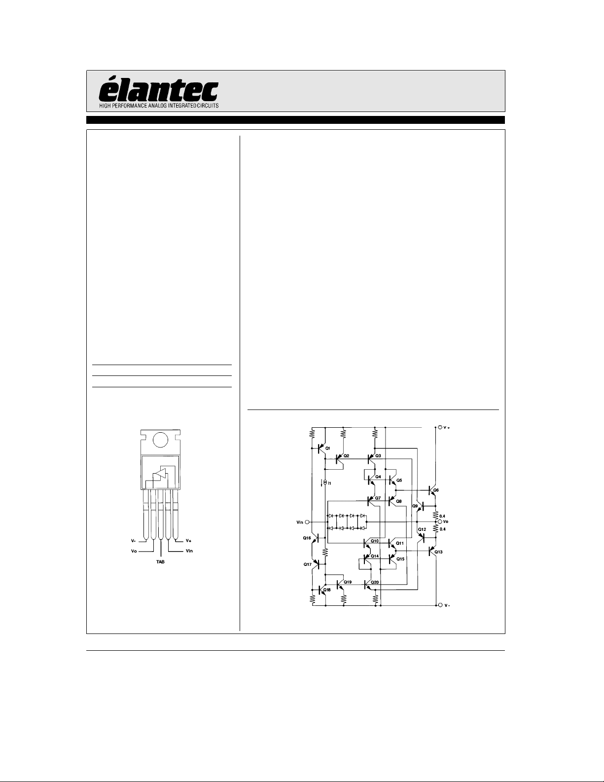
Connection Diagram
5-Pin TO-220
General Description
The EL2009 is a patented high speed bipolar monolithic buffer
amplifier designed to provide currents over 1 amp at high frequencies, while drawing 40 mA of quiescent supply current. The
EL2009’s 3000 V/ms slew rate and 90 MHz bandwidth driving a
10X load insures stability in fast op amp feedback loops. Elantec has applied for patents on unique circuitry within the
EL2009.
Used as an open loop buffer, the EL2009’s low output impedance (1X) gives a gain of 0.99 when driving a 100X load and 0.9
driving a 10X load.
The EL2009 has an output short circuit current limit which will
protect the device under both a DC fault condition and AC operation with reactive loads.
The EL2009 is constructed using Elantec’s proprietary Complementary Bipolar process that produces PNP and NPN transistors with essentially identical AC and DC characteristics. In the
EL2009, the Complementary Bipolar process also insulates the
package’s metal heat sink tab from all supply voltages. Therefore, the tab may be mounted to an external heat sink or the
chassis without an insulator.
Ý
The EL2009CT is specified for operation over the 0
temperature range and is provided in a 5-lead TO-220 plastic
power package.
Simplified Schematic
Ctoa75§C
§
Top View
Note: All information contained in this data sheet has been carefully checked and is believed to be accurate as of the date of publication; however, this data sheet cannot be a ‘‘controlled document’’. Current revisions, if any, to these
specifications are maintained at the factory and are available upon your request. We recommend checking the revision level before finalization of your design documentation.
©
1989 Elantec, Inc.
2009– 1
2009– 2
Manufactured under U.S. Patent No. 4,833,424 and 4,827,223 and U.K. Patent No.
2217134.
Page 2

EL2009C
90 MHz 1 Amp Buffer Amplifier
Absolute Maximum Ratings
V
S
V
IN
I
IN
P
D
Important Note:
All parameters having Min/Max specifications are guaranteed. The Test Level column indicates the specific device testing actually
performed during production and Quality inspection. Elantec performs most electrical tests using modern high-speed automatic test
equipment, specifically the LTX77 Series system. Unless otherwise noted, all tests are pulsed tests, therefore T
Test Level Test Procedure
Supply Voltage (VabVb)
Input Voltage (Note 1)
Input Current (Note 1)
Power Dissipation (Note 2) See Curves
I 100% production tested and QA sample tested per QA test plan QCX0002.
II 100% production tested at T
III QA sample tested per QA test plan QCX0002.
IV Parameter is guaranteed (but not tested) by Design and Characterization Data.
V Parameter is typical value at T
T
MAX
and T
MIN
A
per QA test plan QCX0002.
Electrical Characteristics
Parameter Description
V
OS
I
IN
R
IN
A
V1
A
V2
A
V3
V
O1
V
O2
R
O1
R
O2
I
O
I
S
Output Offset Voltage 0
Input Current 0
Input Impedance
Voltage Gain
Voltage Gain
Voltage Gain,
e
g
5V
V
S
Output Voltage Swing
Output Voltage Swing
Output Impedance
Output Impedance
Output Current
Supply Current 0
PSRR Supply Rejection
(Note 4)
V
IN
g
12V 100X 25§C 250 900 I kX
g
10V
g
10V 10X 25§C 0.88 0.90 I V/V
g
3V 10X 25§C 0.87 0.89 I V/V
g
14V 100X 25§C
g
12V 10X 25§C
g
10Vg10 mA 25§C 1.5 I X
g
10V
g
12V (Note 3) 25§C 1.4 1.8 I A
0
e
(T
25§C)
A
g
18V or 36V
g
15V or V
S
g
50 mA
e
25§C and QA sample tested at T
e
25§C for information purposes only.
A
e
g
V
S
15V, R
e
50X, unless otherwise specified
S
Operating Temperature Range 0§Ctoa75§C
T
A
T
Operating Junction Temp. 175§C
J
T
Storage Temp. Range
ST
T
Lead Solder Temp.k10 seconds 300§C
LD
e
25§C,
A
Test Conditions Limits
Load Temp Min Typ Max
%
%
%
g
1A 25§C 0.9 1.0 I X
%
%
25§C
T
MIN,TMAX
25§C
T
MIN,TMAX
25§C 0.985 0.999 I V/V
T
MIN,TMAX
25§C304565ImA
25
C60 IdB
§
b
60 60 I mV
b
80 80 IV mV
b
125
b
200 200 IV mA
g
13 I V
g
10.5
1IVA
b
65§Ctoa150§C
e
e
T
TA.
J
C
Test
Level
b
5 125 I mA
g
11 I V
Units
TDis 3.6in
2
Page 3
EL2009C
90 MHz 1 Amp Buffer Amplifier
e
Electrical Characteristics
Parameter Description
a
b
V
,V
S
SR
1
SR
2
tr,t
f
BW
C
IN
THD Total Harmonic Distortion 25§C1I%
Note 1: If the input exceeds the ratings shown (or the supplies) or if the input voltage exceedsg7.5V then the input current must be
limited to
Note 2: The maximum power dissipation depends on package type, ambient temperature and heat sinking. See the characteristic
curves for more details.
Note 3: Force the input to
the output.
Note 4: V
Note 5: V
a
Note 6: Slew Rate is measured between V
Note 7: Slew Rate is measured between V
Voltage Gain and
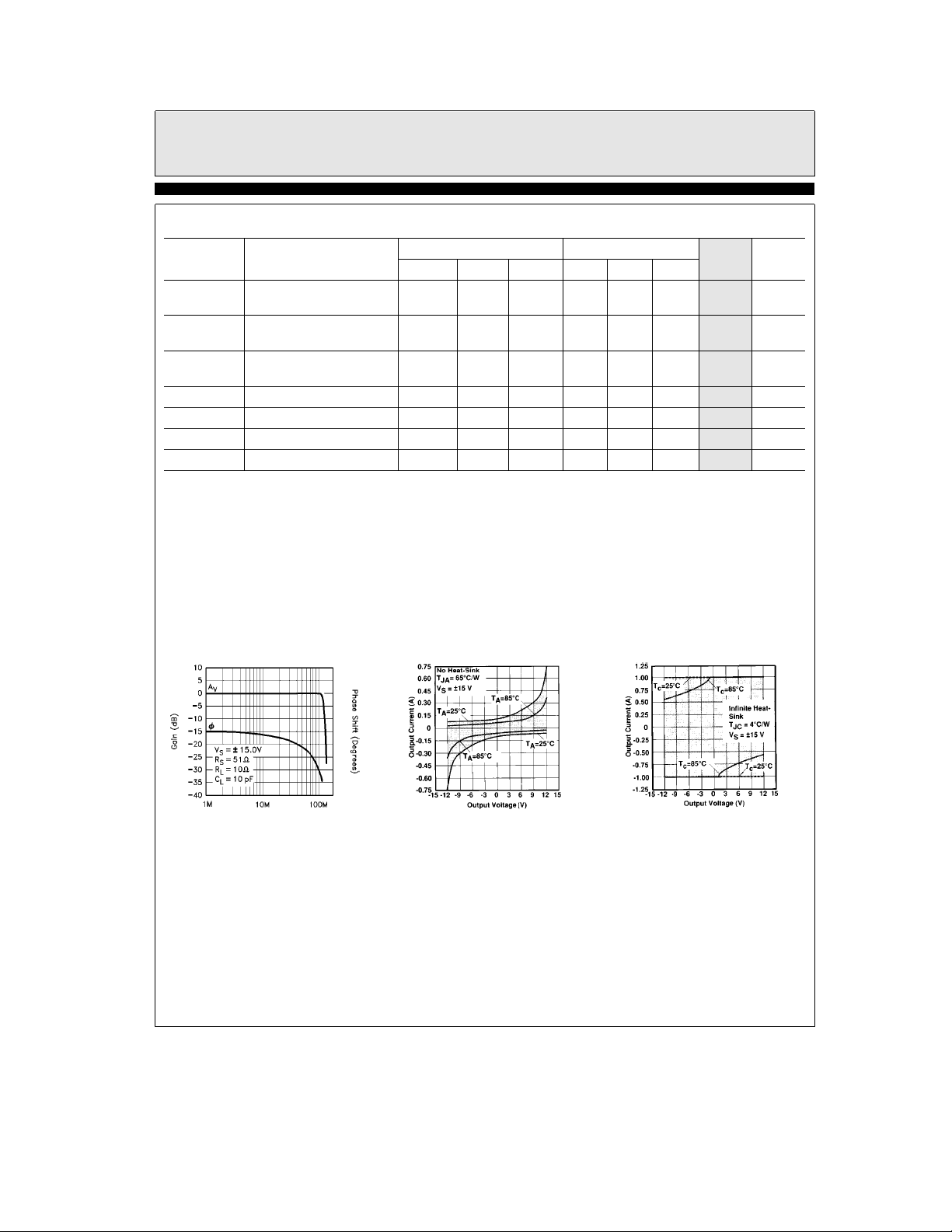
Phase vs Frequency
Supply Sensitivity
S
(Note 5)
Slew Rate
(Note 6) 10X 2500
Slew Rate
(Note 7)
Rise/Fall Time 100 mV 10X 25§C7 Vns
b
3 dB Bandwidth 100 mV 10X 25§C 90 V MHz
Input Capacitance 25§C25 VpF
g
50 mA.
a
12V and the output toa10V and measure the output current. Repeat withb12V input andb10V on
e
g
4.5V then VSis changed tog18V.
S
aea
S
18V.
15V, V
be
S
4.5V then V
OUT
OUT
g
V
S
V
IN
g
10V 50X 25§C 3000
g
5V 10X 25§C 1250 V V/ms
b
is changed tob18V and V
S
ea
5V andb5V.
ea
2.5V andb2.5V.
e
15V, R
Test Conditions Limits
Active operating area Active operating area
50X, unless otherwise specified Ð Contd.
S
Load Temp Min Typ Max
%
C 2 I mV/V
25
§
beb
S
15V, V
aea
S
4.5V then V
Test
Level
VV/ms
a
is changed to
S
Units
TDis 2.1in
2009– 4
Applications Information
The EL2009 is a higher bandwidth of the
EL2008. It is recommended that you read the
EL2008 application section.
Video Distribution Amplifier
The EL2009 can drive 15 double matched 75X
cables. If the EL2009 is used within an op amp
feedback loop the output levels are independent
of loading. The circuit below accepts 1 of 2 inputs
2009– 5
and drives 15 cables. Pin 8 of the EL2020 (Disable) is used to multiplex between the inputs and
can be easily expanded to accept more inputs.
The circuit as shown when fully loaded has differential phase
k
0.1%. The 100X resistor at the EL2009 input
k
0.1§and differential gain
(R1) is necessary to stabilize the loop. The
EL2009 operates with a CLASS AB output which
exhibits a slight rise in output impedance when-
3
2009– 6
Page 4

EL2009C
90 MHz 1 Amp Buffer Amplifier
Applications Information
ever the current it sources into the load approaches zero. In those cases, where differential
gain and phase are measurably affected, resistor
R2 may be added to ensure that the EL2009 out-
Ð Contd.
Video Mux and Distribution Amp.
put current never reaches zero. This will result in
a CLASS A output stage with active pulldown
but with the penalty of power dissipation in R2.
More information about driving cables can be
found in the EL2003 data sheet.
2009– 3
4
Page 5

EL2009 Macromodel
EL2009C
90 MHz 1 Amp Buffer Amplifier
* Connections:
*
*
*
*
.subckt M2009 4512
*
*Input Stage
*
e1100401.0
r1 10 0 1K
rh 10 11 1K
ch 11 0 1pF
rc 11 12 6.3K
cc 12 0 0.159pF
e2 13 0 12 0 1.0
*
* Output Stage
*
q111314qp
q251315qn
q351416qn10
q411519qp10
r2 16 2 0.2
r3 19 2 0.2
c1 14 0 1.7pF
c1 15 0 1.7pF
i15145mA
i2 15 1 5mA
*
* Bias Current
*
a
iin
405mA
*
*Models
*
.model qn npn (is
.model qp pnp (is
*
.ends
a
input
a
l
ll
lll
Vsupply
b
Vsupply
output
llll
e5eb
15 bfe500)
e5eb
15 bfe500)
TDis 5.3in
5
Page 6

BLANK
6
Page 7

BLANK
7
Page 8

EL2009C
90 MHz 1 Amp Buffer Amplifier
EL2009CDecember 1995 Rev C
Package Outline
MDP0028 Rev. A
5-Pin TO-220 Package
General Disclaimer
Specifications contained in this data sheet are in effect as of the publication date shown. Elantec, Inc. reserves the right to make changes
in the circuitry or specifications contained herein at any time without notice. Elantec, Inc. assumes no responsibility for the use of any
circuits described herein and makes no representations that they are free from patent infringement.
WARNING Ð Life Support Policy
Elantec, Inc. products are not authorized for and should not be
used within Life Support Systems without the specific written
consent of Elantec, Inc. Life Support systems are equipment in-
Elantec, Inc.
1996 Tarob Court
Milpitas, CA 95035
Telephone: (408) 945-1323
(800) 333-6314
Fax: (408) 945-9305
European Office: 44-71-482-4596
tended to support or sustain life and whose failure to perform
when properly used in accordance with instructions provided can
be reasonably expected to result in significant personal injury or
death. Users contemplating application of Elantec, Inc. products
in Life Support Systems are requested to contact Elantec, Inc.
factory headquarters to establish suitable terms & conditions for
these applications. Elantec, Inc.’s warranty is limited to replacement of defective components and does not cover injury to persons or property or other consequential damages.
Printed in U.S.A.8
 Loading...