

Page 1
EL2008C
55 MHz 1 Amp Buffer Amplifier
EL2008C
Features
• High slew rate 2500 V/µs
• Wide bandwidth 100MHz @ RL =
50Ω and 55MHz @ RL = 10Ω
• Output current 1A continuous
• Output impedance 1Ω
• Quiescent current 13mA
• Short circuit protected
• Power package with isolated metal
tab
Applications
• Video distribution amplifier
• Fast op amp booster
• Flash converter driver
• Motor driver
• Pulse transformer driver
• A.T.E. pin driver
Ordering Information
Part No. Temp. Range Package Outline#
EL2008CT 0°C to +75°C TO-220 MDP0028
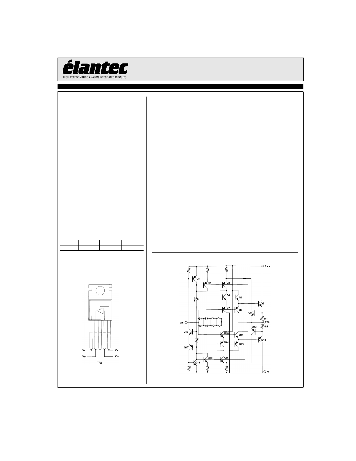
Connection Diagrams
General Description
The EL2008C is a patented high speed bipolar monolithic buffer
amplifier designed to provide currents over 1 amp at high frequencies,
while drawing only 13 mA of quiescent supply current. The
EL2008C's 1500 V/µs slew rate and 55 MHz bandwidth driving a 10Ω
load is second only to the EL2009 and insures stability in fast op amp
feedback loops. Elantec has applied for patents on unique circuitry
within the EL2008C.
Used as an open loop buffer, the EL2008C's low output impedance
(1Ω) gives a gain of 0.99 when driving a 100Ω load and 0.9 driving a
10Ω load. The EL2008C has output short circuit current limiting
which will protect the device under both a DC fault condition and AC
operation with reactive loads.
The EL2008C is constructed using Elantec's proprietary Complementary Bipolar process that produces PNP and NPN transistors with
essentially identical AC and DC characteristics. In the EL2008C, the
Complementary Bipolar process also insulates the package's metal
heat sink tab from all supply voltages. Therefore the tab may be
mounted to an external heat sink or the chassis without an insulator.
The EL2008CT is specified for operation over the 0°C to +75°C temperature range and is provided in a 5-lead TO-220 plastic power
package.
Simplified Schematic
5-Pin TO-220
Top View
Manufactured under U.S. Patent No. 4,833,424 and 4,827,223 and U.K. Patent No. 2217134.
Note: All information contained in this data sheet has been carefully checked and is believed to be accurate as of the date of publication; however, this data sheet cannot be a “controlled document”. Current revisions, if any, to these
specifications are maintained at the factory and are available upon your request. We recommend checking the revision level before finalization of your design documentation.
© 2001 Elantec Semiconductor, Inc.
December 23, 1999
Page 2
EL2008C
55 MHz 1 Amp Buffer Amplifier
EL2008C
Absolute Maximum Ratings (T
V
S
V
IN
If the input exceeds the ratings shown (or the supplies) or if the input voltage exceeds ±7.5V
then the input current must be limited to ±50 mA. See the application hints for information.
I
IN
P
D
Supply Voltage (V+ - V-) ±18V or 36V
Input Voltage ±15 or V
Input Current (See note above) ±50 mA
Power Dissipation See Curves
= 25°C)
A
The maximum power dissipation depends on package type, ambient temperature and heat
sinking. See the characteristic curves for more details.
S
T
A
T
J
T
ST
T
LD
Operating Temperature Range 0°C to +75°C
Operating Junction Temp 175°C
Storage Temp Range -65°C to +150°C
Lead Solder Temp <10 seconds 300°C
Important Note:
All parameters having Min/Max specifications are guaranteed. The Test Level column indicates the specific device testing actually performed during
production and Quality inspection. Elantec performs most electrical tests using modern high-speed automatic test equipment, specifically the LTX77
Series system. Unless otherwise noted, all tests are pulsed tests, therefor TJ = TC = TA.
Test Level Test Procedure
I 100% production tested and QA sample tested per QA test plan QCX0002.
II 100% production tested at TA = 25°C and QA sample tested at TA = 25°C, T
MAX
and T
per QA test plan QCX0002.
MIN
III QA sample tested per QA test plan QCX0002.
IV Parameter is guaranteed (but not tested) by Design and Characterization Data.
V Parameter is typical value at TA = 25°C for information purposes only.
Electrical Characteristics
VS = ±15V, R
Parameter Description
V
OS
I
IN
R
IN
A
V1
A
V2
A
V3
V
01
V
02
R
01
R
02
I
O
I
S
PSRR Supply Rejection
VS+, VS- Supply Sensitivity
SR
SR
tr, t
= 50Ω, unless otherwise specified
S
Output Offset Voltage 0 × 25°C -40 10 +40 I mV
Input Current 0 × 25°C -35 -5 +35 I µA
Input Impedance ±12V 100Ω 25°C 0.5 2 I MΩ
Voltage Gain
Voltage Gain
Voltage Gain, VS = ±15V
Output Voltage Swing ±14V 100Ω 25°C ±13 I V
Output Voltage Swing ±12V 10Ω 25°C ±10.5 ±11 I V
Output Impedance ±10V ±10 mA 25°C 1.8 2.5 I Ω
Output Impedance ±10V ±1A 25°C 0.8 1.15 I Ω
Output Current ±12V
Supply Current 0 × 25°C 12 17 26 I mA
1
2
f
Slew Rate
Slew Rate
Rise/Fall Time 100 mV 10Ω 25°C 7 V ns
Test Conditions Limits
IN
±10V
±10V
±3V
[2]
[3]
[4]
[5]
0 × 25°C 60 I dB
±10V
±10V
±5V 10Ω 25°C 800 V V/µs
Load Temp Min Typ Max
T
,
-50 +50 IV mV
,
-50 +50 IV µA
0.985
0.88
0.87
,
1 IV A
0.9995
0.91
0.89
10Ω
10Ω
[1]
MIN
T
MAX
T
MIN
T
MAX
×
25°C
25°C
25°C
25°C 1.25 1.8 I A
T
MIN
T
MAX
× 25°C 2 I mV/V
50Ω
10Ω
25°C
25°C
2500
1500
Test Level UnitsV
I
I
I
V
V
V/V
V/V
V/V
V/µs
V/µs
2
Page 3
EL2008C
55 MHz 1 Amp Buffer Amplifier
Electrical Characteristics
VS = ±15V, R
Parameter Description
BW -3 dB Bandwidth 100 mV 10Ω 25°C 55 V MHz
C
IN
THD 25°C 1 I %
1. Force the input to +12V and the output to +10V and measure the output current. Repeat with -12V and -10V on the output.
2. VS = ±4.5V then VS is changed to ±18V.
3. VS+ = +15V, VS- = -4.5V then VS - is changed to -18V and VS- = -15V, VS+ = +4.5V then VS+ is changed to +18V.
4. Slew Rate is measured between V
5. 7:Slew Rate is measured between V
= 50Ω, unless otherwise specified
S
Test Conditions Limits
IN
Input Capacitance 25°C 25 V pF
= +5V and -5V.
OUT
= +2.5V and -2.5V.
OUT
Load Temp Min Typ Max
Test Level UnitsV
EL2008C
3
Page 4
EL2008C
55 MHz 1 Amp Buffer Amplifier
EL2008C
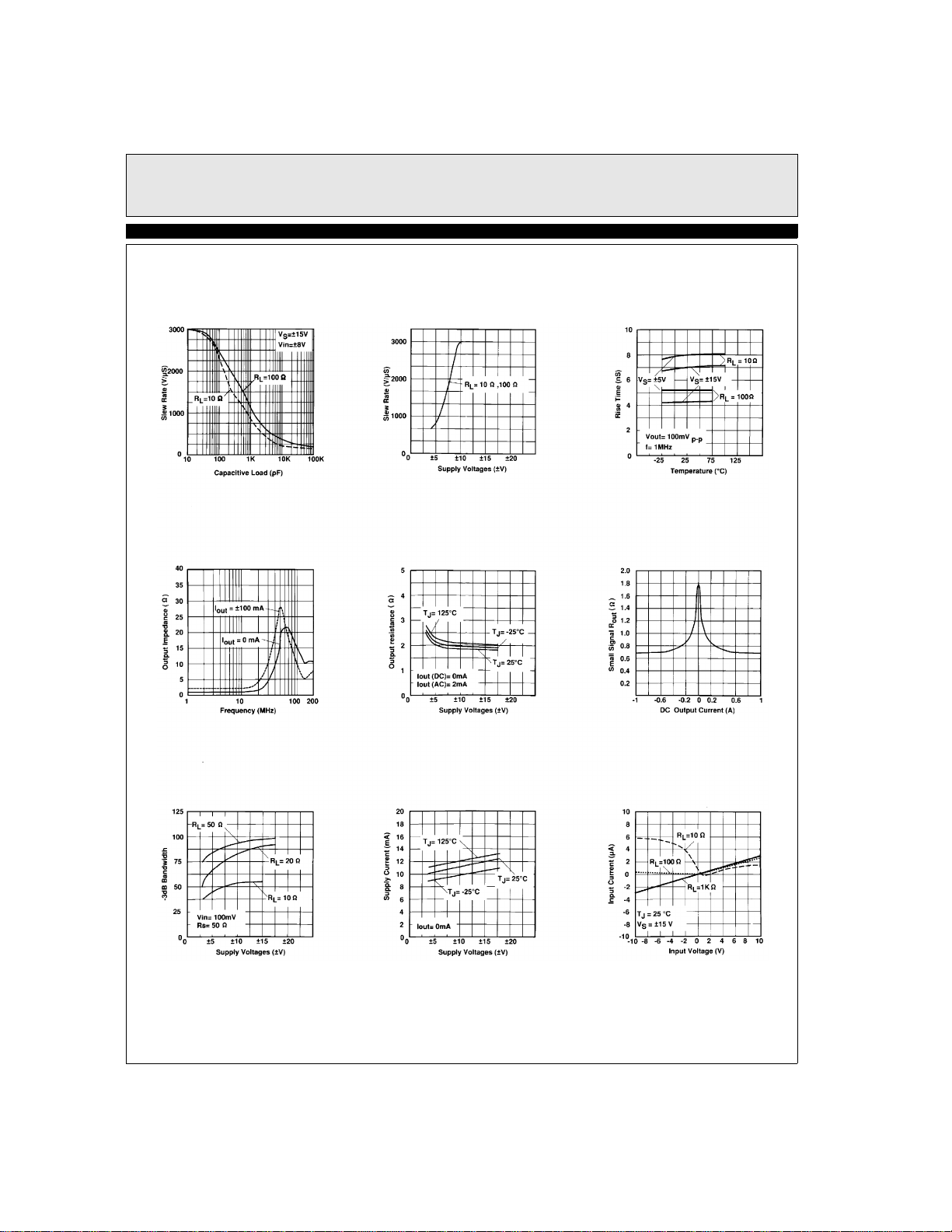
Typical Performance Curves
Slew Rate
vs Capacitance Load
Output Impedance
vs Frequency
Slew Rate
vs Supply Voltage
Output Resistance
vs Supply Voltage
Rise Time
vs Temperature
Small Signal Output
Resistance
vs DC Output Current
-3 dB Bandwidth
vs Supply Voltage
Quiescent Supply Current
vs Supply Voltage
4
Input Current
vs Input Voltage
Page 5

EL2008C
55 MHz 1 Amp Buffer Amplifier
EL2008C
Voltage Gain
vs Frequency at
Various Resistive Loads
Phase Shift
vs Frequency at
Various Resistive Loads
Voltage Gain
vs Frequency at
Various Capacitive Loads
Reverse Isolation
vs Frequency
Voltage Gain
vs Frequency at
Various Capacitive Loads
Power Supply
Rejection Ratio
vs Frequency
Active operating area. Active operating area.
5
Page 6

EL2008C
55 MHz 1 Amp Buffer Amplifier
EL2008C
Burn-In Circuit
Applications Information
The EL2008C is a monolithic buffer amplifier built on
Elantec's proprietary dielectric isolation process that
produces NPN and PNP transistors with essentially
identical DC and AC characteristics. The EL2008C
takes full advantage of the complementary process with
a unique circuit topology.
Elantec has applied for two patents based on the
EL2008C's topology. The patents relate to the base drive
and feedback mechanism in the buffer. This feedback
makes 3000 V/µs slew rates with 10Ω load possible with
modest supply current.
Power Supplies
The EL2008C may be operated with single or split supplies with total voltage difference between 10V (±5V)
and 36V (±18V). However, bandwidth, slew rate and
output impedance are affected by total supply voltages
below 20V (±10V) as shown by the characteristic
curves. It is not necessary to use equal split value supplies. For example -5V and +12V would be excellent for
signals from -2V to +9V.
Bypass capacitors from each supply pin to ground are
highly recommended to reduce supply ringing and the
interference it can cause. At a minimum a 10 µF tantalum capacitor in parallel with a 0.1 µF capacitor with
short leads should be used for both supplies.
Input Characteristics
The input to the EL2008C looks like a resistance in parallel with about 25 pF in addition to a DC bias current.
The DC bias current is due to the mismatch in beta and
collector current between the NPN and PNP transistors
connected to the input pin. The bias current can be either
positive or negative. The change in input current with
input voltage (RIN) is affected by the output load, beta
and the internal boost. RIN can actually appear negative
over portions of the input range in some units. A few
typical input current (IIN) curves are shown in the characteristic curves.
Internal clamp diodes from the input to the output are
provided. These diodes protect the transistor base emitter junctions and limit the boost current during slew to
avoid saturation of internal transistors. The diodes begin
conduction at about ±2.5V input to output differential.
When that happens the input resistance drops dramatically. The diodes are rated at 50 mA. When conducting
6
Page 7

EL2008C
55 MHz 1 Amp Buffer Amplifier
EL2008C
they have a series resistance of about 20Ω. If the output
of the EL2008C is accidentally shorted it is possible that
some devices driving the EL2008C's input could be
damaged or destroyed driving the EL2008C's load
through the diodes while the EL2008C is unaffected. In
such cases a resistor in series with the input of the
EL2008C can limit the current.
Source Impedance
The EL2008C has good input to output isolation. Open
loop, capacitive and resistive sources up to 100 kΩ
present no oscillation problem driving resistive loads as
long as care is used in board layout to minimize output
to input coupling and the supplies are properly bypassed.
When driving capacitive loads in the 100 pF to 1000 pF
region source resistances above 25Ω can cause peaking
and oscillation. Such problems can be eliminated by
placing a capacitor from the EL2008C's input to ground.
The value should be about 1/4 the load capacitance. In a
feedback loop there is a speed penalty and a possibility
of oscillation when the EL2008C is driven with a source
impedance of 200Ω or more. Significant phase shift can
occur due to the EL2008C's 25 pF input capacitance.
Inductive sources can cause oscillations. A series resis-
tor of a few hundred ohms to 1 kΩ will usually solve the
problem.
Current Limit
The EL2008C has internal current limiting to protect the
output transistors. The current limit is about 1.5A at
room temperature and decreases with junction temperature. At 150°C junction temperature it is above 1A.
Heat Sinking
A suitable heat sink will be required for most applications. The thermal resistance junction to case for the TO220 package is 4°C per watt. No voltage appears at the
heat sink tab so no precautions need to be taken to avoid
shorting the tab to a supply voltage or ground. As there
is a small parasitic capacitance between the tab and the
buffer circuitry, it is recommended that the tab be connected to AC ground (either supply voltage or DC
ground). The center lead is internally connected to the
tab so the connection can be made at the tab or the center
lead.
Parallel Operation
If more than 1A is required or if heat management is a
problem, several EL2008Cs may be paralleled together.
The result is as through each device was driving only
part of the load. For example, if two units are paralleled
then a 5Ω load looks like 10Ω to each EL2008C. Of
course, parallel operation reduces both the input and output impedance and increases bias current. But there is no
increase in offset voltage. Three units in parallel can
drive a 3Ω load ±10V at 2500 V/µs. The output impedance will be about 0.33Ω.
Resistive Loads
The DC gain of the EL2008C is the product of the
unloaded gain (0.999) and the voltage divider formed by
the device output resistance and the load resistance.
AV = 0.999* (RL/RL + R
The high frequency response varies with the load resistance as shown by the characteristic curves. Both gain
and phase are shown. If the 80 MHz peaking is undesir-
able when driving load resistors greater than 50Ω, an RC
snubber circuit can be used from output to ground. The
capacitive load section discusses snubber usage in more
detail.
OUT
)
Capacitive Loads
The EL2008C is not stable driving purely capacitive
loads between 100 pF and 500 pF. Purely capacitive
loads from 500 pF to 1000 pF will also have excessive
peaking as shown in the characteristic curves. The
squarewave response will have large overshoots and
ring for hundreds of nanoseconds.
When driving capacitive loads, stability can be achieved
and peaking and ringing can be minimized either by add-
ing a 50Ω (or less) load in parallel with the capacitive
load or by an RC snubber circuit from output to ground.
The snubber values can be found empirically by observing a squarewave or the frequency response. First just
put a resistor alone from the output to ground until the
desired response is achieved. The gain will be reduced
due to the output resistance of the EL2008C and power
consumption will be high. Then put a capacitor in series
with the resistor to restore gain at low frequencies and
eliminate the DC current. Start with a small capacitor
and increase until the response is optimum. The figure
7
Page 8

EL2008C
55 MHz 1 Amp Buffer Amplifier
EL2008C
below shows an example of an EL2008C driving a 100
pF load.
Driving a pure capacitive load. Top trace is without a snubber.
Bottom trace is with a snubber circuit.
frequency compensation is required. An op amp fol-
lowed with the EL2008C can drive loads as low as 10Ω
to ±10V.
Driving capacitive loads with any closed loop system
creates special problems. The open loop output impedance works into the load capacitance to generate phase
lag which can make the loop unstable. The EL2008C
output impedance is less than 10Ω from DC to 30 MHz.
But a capacitive load of 1000 pF will generate about 45
degrees of phase shift at 30 MHz. More capacitance will
cause the problem at lower frequency.
With enough capacitance even slow op amps will
become unstable. The simplest way to drive capacitive
loads is to isolate them from the feedback with a series
resistor. 1Ω to 5Ω is usually enough but the final value
will depend on the op amp used and the range of load
capacitance.
Inductive Loads
The EL2008C with its 1A output current can drive small
motors and other inductive loads. The EL2008C's current limiting into inductive loads does NOT in and of
itself cause spikes and kickbacks. However, if the
EL2008C is in current limit and the input voltage is
changing very quickly (i.e., a squarewave) the inductive
load can kick the output beyond the supply voltages.
Motors are also able to generate kickback voltages when
the EL2008C is in current limit.
To prevent damage to the EL2008C when the output
kicks beyond the supplies it is recommended that catch
diodes be placed from each supply to the output.
Op Amp Booster
The EL2008C can boost the output drive of almost any
monolithic op amp. If the phase shift in the EL2008C is
low at the op amp's unity gain frequency, no additional
C
L
13 pF
470 pF
1000 pF
3300 pF
0.1 µF
1 µF
5 µF
t
r
45 ns
50 ns
55 ns
60 ns
350 ns
4 µs
20 µs
O.S.
20%
20%
30%
30%
0%
0%
0%
Unfortunately the isolation resistor is not inside the op
amp feedback loop and cannot be neglected when computing the DC voltage gain into a resistive load. If load
dependent DC gain is not tolerable then additional high
frequency feedback from the op amp output (the
EL2008C input) and an isolation resistor from the buffer
output can be used to stabilize the loop. This configuration requires the op amp to be unity gain stable. This
feedback method will allow the EL2008C to boost the
output of the EHA2505 amplifier below and serve as a
8
Page 9

EL2008C
55 MHz 1 Amp Buffer Amplifier
EL2008C
variable, bipolar 1A voltage supply with short circuit
protection.
Slew Rate = 1A/C
L
Video Distribution Amplifier
The EL2008C can drive 15 double matched 75Ω cables.
If the EL2008C is used within an op amp feedback loop
the output levels are independent of loading. The circuit
below accepts 1 of 2 inputs and drives 15 cables. Pin 8 of
the EL2020 (Disable) is used to multiplex between the
inputs and can be easily expanded to accept more inputs.
The circuit as shown when fully loaded has differential
phase <0.1° and differential gain <0.1%. The 100Ω
resistor at the EL2008C input (R1) is necessary to stabi-
lize the loop. The 100Ω resistor at the EL2008C output
(R2) to the -12V supply, insures that the EL2008C
sources current even when the output voltage is at 0V.
This is necessary to achieve the excellent differential
gain and phase values. More information about driving
cables can be found in the EL2003 data sheet. See the
EL2020 data sheet to learn more about using it as a
multiplexer.
Input (top trace) and output (bottom trace)
of EHA2505 op amp boosted by EL2008C.
9
Page 10

EL2008C
55 MHz 1 Amp Buffer Amplifier
EL2008C
Video Mux and Distribution Amplifier
10
Page 11

EL2008C Macromodel
* Connections: +input
* | +Vsupply
* | | -Vsupply
* | | | output
* | | | |
.subckt M2008 4 5 1 2
*
* Input Stage
*
e1 10 0 4 0 1.0
r1 10 0 1K
rh 10 11 1K
ch 11 0 2.65pF
rc 11 12 10K
cc 12 0 0.159pF
e2 13 0 12 0 1.0
*
* Output Stage
*
q1 1 13 14 qp
q2 5 13 15 qn
q3 5 14 16 qn 15
q4 1 15 19 qp 15
r2 16 2 0.4
r3 19 2 0.4
c1 14 0 0.6pF
c2 15 0 0.6pF
i1 5 14 1.2mA
i2 15 1 1.2mA
*
* Bias Current
*
iin+ 4 0 5µA
*
* Models
*
.model qn npn (is=5e-15 bf=1500)
.model qp pnp (is=5e-15 bf=1500)
.ends
EL2008C
EL2008C
55 MHz 1 Amp Buffer Amplifier
11
Page 12

EL2008C
55 MHz 1 Amp Buffer Amplifier
EL2008C
General Disclaimer
Specifications contained in this data sheet are in effect as of the publication date shown. Elantec, Inc. reserves the right to make changes in the circuitry or specifications contained herein at any time without notice. Elantec, Inc. assumes no responsibility for the use of any circuits described
herein and makes no representations that they are free from patent infringement.
WARNING - Life Support Policy
Elantec, Inc. products are not authorized for and should not be used
within Life Support Systems without the specific written consent of
Elantec, Inc. Life Support systems are equipment intended to sup-
Elantec Semiconductor, Inc.
675 Trade Zone Blvd.
Milpitas, CA 95035
Telephone: (408) 945-1323
(888) ELANTEC
Fax: (408) 945-9305
European Office: +44-118-977-6020
Japan Technical Center: +81-45-682-5820
port or sustain life and whose failure to perform when properly used
in accordance with instructions provided can be reasonably
expected to result in significant personal injury or death. Users contemplating application of Elantec, Inc. Products in Life Support
Systems are requested to contact Elantec, Inc. factory headquarters
to establish suitable terms & conditions for these applications. Elantec, Inc.’s warranty is limited to replacement of defective
components and does not cover injury to persons or property or
other consequential damages.
December 23, 1999
12
Printed in U.S.A.
 Loading...