

Page 1
EL2006/EL2006A November 1993 Rev F
EL2006/EL2006A
High Gain Fast FET Input Op Amp
Note: All information contained in this data sheet has been carefully checked and is believed to be accurate as of the date of publication; however, this data sheet cannot be a ‘‘controlled document’’. Current revisions, if any, to these
specifications are maintained at the factory and are available upon your request. We recommend checking the revision level before finalization of your design documentation.
©
1989 Elantec, Inc.
Features
# 90 dB open loop gain
# 450 V/ms slew rate
# 40 MHz bandwidth
# No thermal tail
# 3 mV max input offset voltage
# Offset nulls with single pot
# No compensation required for
gains above 50
# Peak output current to 200 mA
# Pin compatible with LH0032
# 80 dB common mode rejection
Ordering Information
Part No. Temp. Range Pkg. Outline
Ý
EL2006CG
b
25§Ctoa85§C TO-8 MDP0002
EL2006G
b
55§Ctoa125§C TO-8 MDP0002
EL2006G/883Bb55§Ctoa125§C TO-8 MDP0002
EL2006ACG
b
25§Ctoa85§C TO-8 MDP0002
EL2006AG
b
55§Ctoa125§C TO-8 MDP0002
EL2006AG/883Gb55§Ctoa125§C TO-8 MDP0002
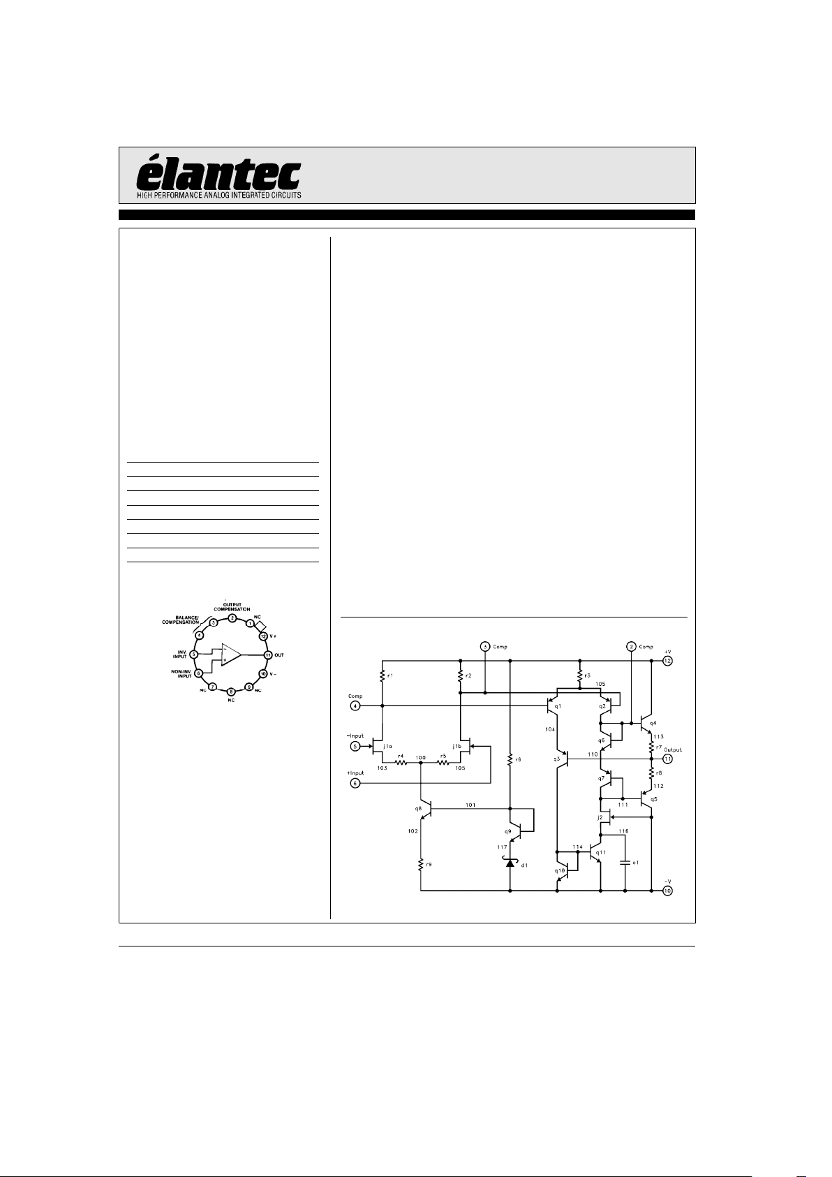
Connection Diagrams
2006– 1
Top View
General Description
The EL2006/EL2006A are high slew rate, wide bandwidth, high
input impedance, high gain and fully differential input operational amplifiers. They exhibit excellent open loop gain characteristics making them suitable for a broad range of high speed
signal processing applications. These patented devices have
open loop gains in excess of 86 dB making the EL2006/
EL2006A ideal choices for current mode video bandwidth digital to analog converters of 10 bits or higher resolution. The
EL2006’s FET input structure, high slew rate, and high output
drive capability allow use in applications such as buffers for
flash converter inputs. In general, the EL2006/EL2006A allow
the user to take relatively high closed loop gains without compromising gain accuracy or bandwidth.
The EL2006/EL2006A are pin compatible with the popular industry standard ELH0032/ELH0032A offering comparable
bandwidth and slew rate, while offering significant improvements in open loop gain, common mode rejection and power
supply rejection.
Elantec facilities comply with MIL-I-45208A and are
MIL-STD-1772 certified. Elantec’s Military devices comply
with MIL-STD-883 Class B Revision C and are manufactured
in our rigidly controlled, ultra-clean facilities in Milpitas, California. For additional information on Elantec’s Quality and Reliability Assurance Policy and procedures request brochure
QRA-1.
Simplified Schematic
2006– 3
Manufactured under U.S. Patent No. 4,746,877
Page 2
EL2006/EL2006A
High Gain Fast FET Input Op Amp
Absolute Maximum Ratings
(T
A
e
25§C)
V
S
Supply Voltage
g
18V
V
IN
Input Voltage
g
15V
Differential Input Voltage 30V
I
OUT
Peak Output Current (Note 1)
g
200 mA
P
D
Power Dissipation
T
A
e
25§C 1.5W, derate 100§C/W toa125§C
T
C
e
25§C 2.2W, derate 70§C/W toa125§C
T
A
Operating Temperature Range
EL2006, EL2006A
b
55§Ctoa125§C
EL2006C, EL2006AC
b
25§Ctoa85§C
T
J
Operating Junction Temperature 175§C
T
ST
Storage Temperature
b
65§Ctoa150§C
Lead Temperature
(Soldering 10 seconds) 300
§
C
Important Note:
All parameters having Min/Max specifications are guaranteed. The Test Level column indicates the specific device testing actually
performed during production and Quality inspection. Elantec performs most electrical tests using modern high-speed automatic test
equipment, specifically the LTX77 Series system. Unless otherwise noted, all tests are pulsed tests, therefore T
J
e
T
C
e
TA.
Test Level Test Procedure
I 100% production tested and QA sample tested per QA test plan QCX0002.
II 100% production tested at T
A
e
25§C and QA sample tested at T
A
e
25§C,
T
MAX
and T
MIN
per QA test plan QCX0002.
III QA sample tested per QA test plan QCX0002.
IV Parameter is guaranteed (but not tested) by Design and Characterization Data.
V Parameter is typical value at T
A
e
25§C for information purposes only.
DC Electrical Characteristics
V
S
e
g
15V, T
MIN
k
T
A
k
T
MAX
EL2006 EL2006C
Parameter Description Test Conditions
Min Typ Max
Test
Min Typ Max
Test Units
Level Level
V
OS
Offset Voltage T
J
e
25§C5I5ImV
10 I 10 III mV
DVOS/DT Offset Voltage Drift 15 V 15 V mV/§C
I
B
Bias Current T
J
e
25§C 100 I 500 I pA
1 10 I 1 10 III nA
I
OS
Offset Current T
J
e
25§C 25 I 50 I pA
0.2 2.5 I 0.2 2.5 III nA
V
CM
Common Mode Range
g
10 I
g
10 II V
CMRR Common Mode DV
IN
e
g
10V
70 80 I 70 80 II dB
Rejection Ratio
PSRR Power Supply
g
5VsV
S
s
g
15V
70 88 I 70 88 II dB
Rejection Ratio
A
VOL
Large Signal R
L
e
1kX,V
OUT
e
g
10V,
74 90 I 74 90 I dB
Voltage Gain T
J
e
25§C
R
L
e
1kX,V
OUT
e
g
10V 80 I 74 III dB
V
O
Output Voltage Swing R
L
e
1kX
g
12 I
g
12 II V
I
OUT
Output Current V
OUT
e
g
10V,
g
100 Ig100 I mA
T
J
e
25§C, (Note 1)
I
CC
Supply Current 20 23 I 20 23 II mA
2
TDis 0.9inTDis 3.9in
Page 3
EL2006/EL2006A
High Gain Fast FET Input Op Amp
DC Electrical Characteristics
Ð Contd.
V
S
e
g
15V, T
MIN
k
T
A
k
T
MAX
(Note: These tests are in addition to those listed above.)
EL2006A EL2006AC
Parameter Description Test Conditions
Min Typ Max
Test
Min Typ Max
Test Units
Level Level
V
OS
Offset Voltage T
J
e
25§C3I3ImV
DV
OS
/DT Offset Voltage Drift 15 25 I 15 25 I mV/§C
A
VOL
Large Signal T
J
e
25§C, R
L
e
1kX,
74 90 I 74 90 II dB
Voltage Gain V
OUT
e
g
10V
R
L
e
1kX,V
OUT
e
g
10V 74 I 74 III dB
AC Electrical Characteristics
V
S
e
g
15V, R
L
e
1kX,T
J
e
25§C (See AC Test Circuits)
EL2006, EL2006A EL2006C, EL2006AC
Parameter Description Test Conditions
Min Typ Max
Test
Min Typ Max
Test Units
Level Level
t
r
Rise Time A
V
e
10V, V
OUT
e
1V
P-P
18 V 18 V ns
A
V
e
1V, V
OUT
e
1V
P-P
12 15 I 12 15 I ns
SR Slew Rate (Note 2) A
V
e
1V, V
OUT
e
20 V
P-P
350 450 I 350 450 I V/ms
t
s
Settling Time to 1.0% A
V
eb
1V, V
OUT
e
10 V
P-P
90 V 90 V ns
t
s
Settling Time to 0.1% A
V
eb
1V, V
OUT
e
10 V
P-P
160 V 160 V ns
t
s
Settling Time to 0.01% A
V
eb
1V, V
OUT
e
10 V
P-P
250 V 250 V ns
GBW Gain Bandwidth Product A
V
t
20V 500 V 500 V MHz
Pull Power V
OUT
e
g
10V
5.5 7 I 5.5 7 I MHz
Bandwidth (Note 3)
Unity Gain Bandwidth C
A
e
8 pF, C
B
e
100 pF 40 V 40 V MHz
e
N
Noise Voltage 1 kHz to 1 MHz 20 V 20 V nV/0Hz
t
D
Small Signal Delay A
V
e
1V 13 15 I 13 15 I ns
C
IN
Input Capacitance 2 V 2 V pF
Note 1: T
J
e
25§C, duty cyclek1%, pulse widthk10 ms.
Note 2: Slew rate is measured at the 25% and 75% points.
Note 3: The Full Power bandwidth is guaranteed by testing slew rate.
EL2006 Recommended Compensation
(See Figure 1)
A
VOL
C
A
C
B
R
S
a
R
S
b
R
F
a
1 5–8 pF 100 pF 2k Open Circuit 100
b
1toa5 5 pF 68 pF 0
k
1k 1k
g
10 5pF 10pF
k
1k 1k
l
10k
l
g
20 3pF 10pF
k
1k 1k
l
20k
Note: Use a small capacitor of about 1 pF in parallel with RFto compensate for stray
input capacitance.
2006– 4
Figure 1
3
TDis 1.4inTDis 2.9in
Page 4
EL2006/EL2006A
High Gain Fast FET Input Op Amp
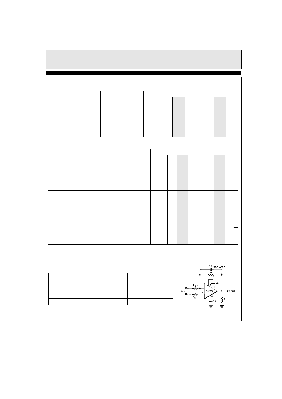
Typical Performance Curves
Bode Plot, Unity Gain
Compensation
Supply Current vs
Temperature
Inverting Gain ofb1
Settling Time
Voltage
Function of Input
Input Bias Currents as a
Dissipation
Maximum Power
TO-8
Junction Temperature
and Offset Current vs
Normalized Input Bias
2006– 5
Applications Information
General
The EL2006 was designed to overcome the gain
and stability limitations of prior high speed FET
input operational amplifiers like the LH0032.
Open loop gain is typically 90 dB allowing gain
setting to 12-bit accuracy. This new design also
eliminates ‘‘thermal tail’’, which is the tendency
for the gain to diminish at very low frequencies
to DC due to thermal feedback. The EL2006 is
also easier to stabilize than earlier designs,
thanks to an Elantec proprietary internal compensation technique which eliminates the ‘‘second stage bump.’’ The EL2006 open loop gain
4
Page 5

EL2006/EL2006A
High Gain Fast FET Input Op Amp
Applications Information
Ð Contd.
characteristic is well behaved well beyond the
unity gain frequency so that spurious ringing or
oscillation in the 100 MHZ – 200 MHz region is
avoided. Finally, we have provided temperature
compensation so that gain and stability are relatively constant over temperature.
These improvements are provided in a configuration which is plug compatible with LH0032 and
similar products so that designers can easily upgrade their system performance without extensive re-design. In most cases, the EL2006 can be
used to replace LH0032 with no change in external compensation.
Video DAC Amplifiers
A typical application for the EL2006 is to provide gain for video signals. In the example
shown, the EL2006 provides a gain of 2 with settling time around 35 ns to 10 mV.
Power Supply Decoupling
The EL2006/EL2006A, like most high-speed circuits, is sensitive to layout and stray capacitance.
Power supplies should be bypassed as near to
pins 10 and 12 as possible with low inductance
capacitors such as 0.01 mF disc ceramics. Compensation components should also be located
close to the appropriate pins to minimize stray
reactances.
Input Current
Because the input devices are FETs, the input
bias current may be expected to double for each
11
§
C junction temperature rise. This characteristic is plotted in the typical performance characteristics graphs. The device will self-heat due to
internal power dissipation after application of
power, thus raising the FET junction temperature 40
§
C–60§C above the free-air ambient tem-
perature when supplies are
g
15V. The device
temperature will stabilize within 5–10 minutes
after application of power, and the input bias currents measured at the time will be indicative of
normal operating currents. An additional rise will
occur as power is delivered to a load due to additional internal power dissipation.
Power Dissipation
There is an additional effect on input bias current
as the input voltage is changed. The effect, common to all FETs, is an avalanche-like increase in
gate current as the FET gate-to-drain voltage is
increased above a critical value, depending on
FET geometry and doping levels. This effect will
be noted as the input voltage of the EL2006 is
taken below ground potential when the supplies
are
g
15V. All of the effects described here may
be minimized by operating the device with
V
S
s
g
15V.
These effects are indicated in the typical performance curves.
Input Capacitance
The input capacitance to the EL2006/EL2006A
is typically 2 pF and thus may form a significant
time constant with high value resistors. For optimum performance, the input capacitance to the
inverting input should be compensated by a
small capacitor across the feedback resistor. The
value is strongly dependent on layout and closed
loop gain, but will typically be in the neighborhood of several picofarads.
In the non-inverting configuration, it may be advantageous to bootstrap the case and/or a guard
conductor to the inverting input. This serves
both to divert leakage currents away from the
non-inverting input and to reduce the effective
input capacitance. A unity gain follower so treated will have an input capacitance undera1pF.
2006– 6
5
Page 6

EL2006/EL2006A
High Gain Fast FET Input Op Amp
Applications Information
Ð Contd.
Heatsinking
While the EL2006/EL2006A are specified for operation without any explicit heatsink, internal
power dissipation does cause a significant temperature rise. Improved bias current performance
can thus be obtained by limiting this tempera-
ture rise with a small heat sink such as the Thermalloy No. 2241 or equivalent. The case of the
device has no internal connection, so it may be
electrically connected to the sink if this is advantageous. Be aware, however, that this will affect
the stray capacitances to all pins and may thus
require adjustment of circuit compensation values.
Voltage Follower (A
V
ea
1)
Large Signal Pulse Response
2006– 12
V
S
e
g
15V, V
IN
ea
10V tob10V andb10V toa10V
Large Signal Pulse Response
Test Circuit
2006– 7
EL2006 Settling Time Test Circuit
2006– 8
Inverting Unity Gain
2006– 9
Inverting Gain of 10
2006– 10
6
Page 7

EL2006/EL2006A
High Gain Fast FET Input Op Amp
Burn-In Circuit
2006– 11
Pin Numbers are for TO-8 package. LCC uses the same schematic.
7
Page 8

EL2006/EL2006A
High Gain Fast FET Input Op Amp
EL2006 Macromodel
* Connections:
a
input
*
l
b
input
*
ll
a
Vsupply
*
lll
b
Vsupply
*
llll
Comp 3
*
lllll
Comp 4
*
llllll
Comp 2
*
lllllll
Output
*
llllllll
.subckt M2006 6 5 12 10 3 4 2 11
* Models
.model qfa njf (vto
eb
2.5V betae1.11eb3 cgde2pF cgse5pF me0.3744)
.model qp pnp (is
e5Eb
14 bfe150 vafe100 ikfe100mA tfe.53nS vtfe0 isee1 nA,
a
cjce4pF cjee5.7pF tre170nS rbe3bre5 mjee.32 mjce.43 xtbe2.1 nee4
a
isce1nA nce4 itfe.4 vtfe4 xtfe6)
.model qn npn (is
e5eb
14 bfe150 vafe800 ikfe200mA tfe.54nS vtfe0
a
cjce4pF cjee5pF rbe3bre5 mjee.42 mjce.23 tre200nS xtbe2.1
a
isee4nA nee4 isce4nA nce4 itfe.4 vtfe4 xtfe2)
.model qfb njf (vto
eb
2.8V betae4eb3 cgde7pF cgse8pF lambdae4eb3)
.model zener d (bv
e
2.49V ibve1mA)
* Resistors and Capacitors
r1 12 4 700
r2 12 3 700
r3 12 105 160
r4 103 100 10
r5 108 100 10
r6 12 101 22K
r7 113 11 10
r8 11 112 10
r9 102 10 407
cs2 10 116 100pF
* Transistors and Diodes
j1a 4 5 103 qfa
j1b 3 6 108 qfa
j2 111 10 116 qfb
q1 104 4 105 qp
q2 2 3 105 qp
q3 114 11 104 qp
q4 12 2 113 qn
q5 10 111 112 qp
q6 2 2 110 qn
q7 111 111 110 qp
q8 100 101 102 qn
d1 10 117 zener
q9 101 101 117 qn
q10 114 114 10 qn
q11 116 114 10 qn
.ends
8
TABWIDE
TDis 6.4in
Page 9

EL2006/EL2006A
High Gain Fast FET Input Op Amp
EL2006 Macromodel
Ð Contd.
2006– 3
9
Page 10

BLANK
10
Page 11

BLANK
11
Page 12

EL2006/EL2006ANovember 1993 Rev F
EL2006/EL2006A
High Gain Fast FET Input Op Amp
General Disclaimer
Specifications contained in this data sheet are in effect as of the publication date shown. Elantec, Inc. reserves the right to make changes
in the circuitry or specifications contained herein at any time without notice. Elantec, Inc. assumes no responsibility for the use of any
circuits described herein and makes no representations that they are free from patent infringement.
Elantec, Inc.
1996 Tarob Court
Milpitas, CA 95035
Telephone: (408) 945-1323
(800) 333-6314
Fax: (408) 945-9305
European Office: 44-71-482-4596
WARNING Ð Life Support Policy
Elantec, Inc. products are not authorized for and should not be
used within Life Support Systems without the specific written
consent of Elantec, Inc. Life Support systems are equipment intended to support or sustain life and whose failure to perform
when properly used in accordance with instructions provided can
be reasonably expected to result in significant personal injury or
death. Users contemplating application of Elantec, Inc. products
in Life Support Systems are requested to contact Elantec, Inc.
factory headquarters to establish suitable terms & conditions for
these applications. Elantec, Inc.’s warranty is limited to replacement of defective components and does not cover injury to persons or property or other consequential damages.
Printed in U.S.A.12
 Loading...