

Page 1
EL2005/EL2005C January 1990 Rev F
EL2005/EL2005C
High Accuracy Fast Buffer
Note: All information contained in this data sheet has been carefully checked and is believed to be accurate as of the date of publication; however, this data sheet cannot be a ‘‘controlled document’’. Current revisions, if any, to these
specifications are maintained at the factory and are available upon your request. We recommend checking the revision level before finalization of your design documentation. Patent pending.
CMSÝ2005DS
©
1989 Elantec, Inc.
Features
# Low input currentÐ50 pA
# Low offset and driftÐ
2 mV/25 mV/
§
C
# High slew rateÐ1500 V/ms
# Fast rise and fall timeÐ2.5 ns
# High input resistanceÐ1000 GX
# BandwidthÐ140 MHz
# Pin compatible with ELH0033
# MIL-STD-883 Revision C devices
manufactured in U.S.A.
Advantages
# No input loading
# Input current independent of
input voltage
# Eliminates offset adjustments
# Drives cables directly
Ordering Information
Part No. Temp. Range Package Outline
Ý
EL2005CGb25§Ctoa85§C TO-8 MDP0002
EL2005G
b
55§Ctoa125§C TO-8 MDP0002
EL2005G/883Bb55§Ctoa125§C TO-8 MDP0002
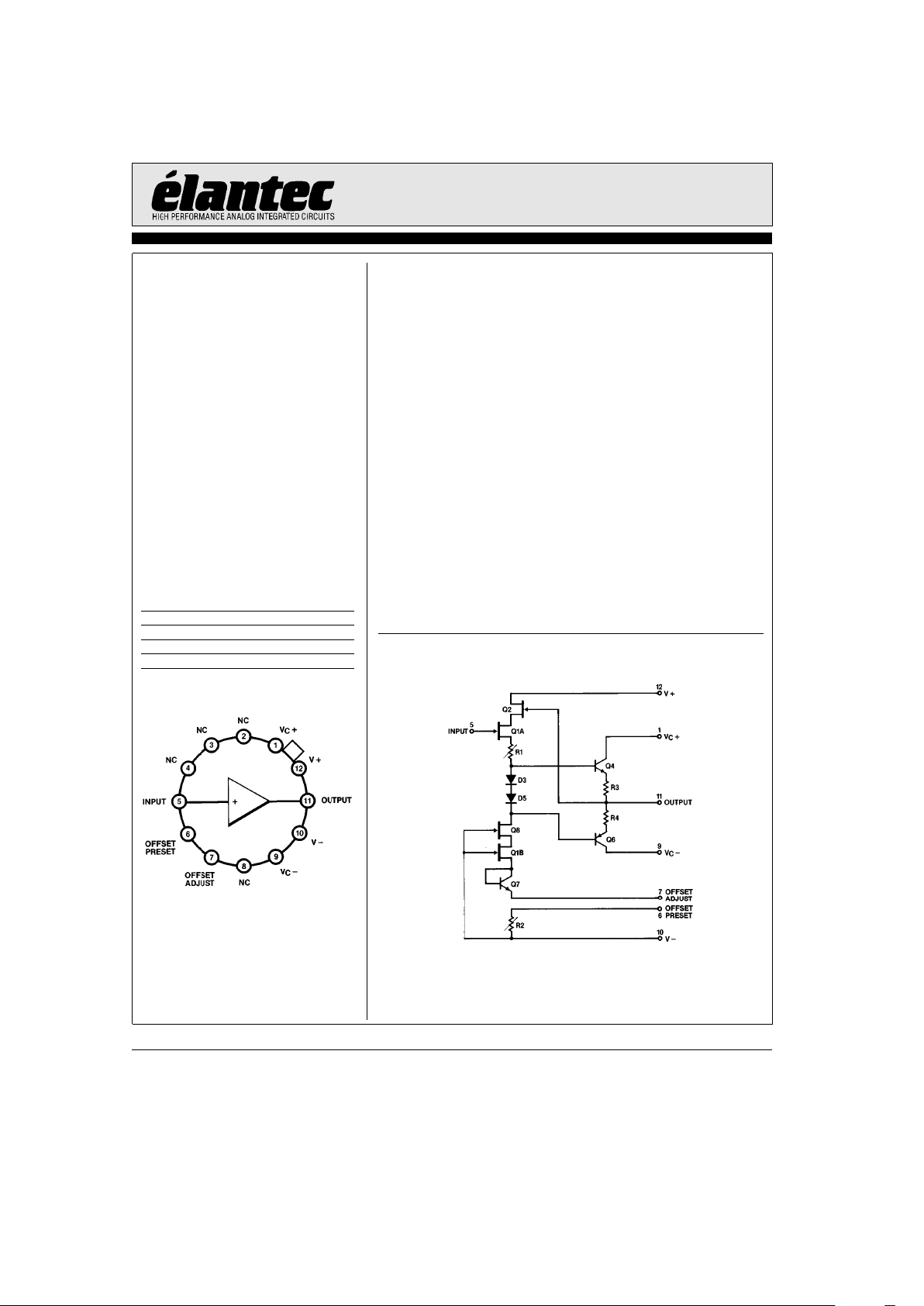
Connection Diagram
2005– 1
Top View
Note: Case is electrically isolated.
General Description
The EL2005 is a high-speed, FET input buffer similar to
ELH0033 and EL2004 but with input specifications significantly improved over the previous types. The input stage employs a
cascode configuration to maintain constant input characteristics over the full
g
10V input range. The input looks likea3pF
capacitor to ground in almost all cases since the DC bias current
is constant with input voltage. In sample and hold circuits this
results in an order of magnitude improvement in hold characteristics. Input offset voltage and offset voltage drift are also
improved a factor of two over previous types.
These excellent DC characteristics are complemented by a wide
140 MHz bandwidth while the 1500 V/ms slew rate and excellent phase linearity of the ELH0033 family are preserved allowing direct plug-in replacement for upgraded performance. (For
even faster operation see EL2004.)
Elantec facilities comply with MIL-I-45208A and are MILSTD-1772 certified. Elantec’s Military devices comply with
MIL-STD-883B Revision C and are manufactured in our rigidly
controlled, ultra-clean facilities in Milpitas, California. For additional information on Elantec’s Quality and Reliability Assurance Policy and procedures request brochure QRA-1.
Simplified Schematic
2005– 2
Page 2
EL2005/EL2005C
High Accuracy Fast Buffer
Absolute Maximum Ratings
(T
A
e
25§C)
V
S
Supply Voltage (VabVb) 40V
V
IN
Input Voltage 40V
P
D
Power Dissipation (See curves) 1.5W
I
OC
Continuous Output Current
g
100 mA
I
OP
Peak Output Current
g
250 mA
T
A
Operating Temperature Range
EL2005
b
55§Ctoa125§C
EL2005C
b
25§Ctoa85§C
T
J
Operating Junction Temperature 175§C
T
ST
Storage Temperature
b
65§Ctoa150§C
Lead Temperature
(Soldering, 10 seconds) 300
§
C
Important Note:
All parameters having Min/Max specifications are guaranteed. The Test Level column indicates the specific device testing actually
performed during production and Quality inspection. Elantec performs most electrical tests using modern high-speed automatic test
equipment, specifically the LTX77 Series system. Unless otherwise noted, all tests are pulsed tests, therefore T
J
e
T
C
e
TA.
Test Level Test Procedure
I 100% production tested and QA sample tested per QA test plan QCX0002.
II 100% production tested at T
A
e
25§C and QA sample tested at T
A
e
25§C,
T
MAX
and T
MIN
per QA test plan QCX0002.
III QA sample tested per QA test plan QCX0002.
IV Parameter is guaranteed (but not tested) by Design and Characterization Data.
V Parameter is typical value at T
A
e
25§C for information purposes only.
DC Electrical Characteristics
V
S
e
g
15V, V
IN
e
0V, T
MIN
s
T
A
s
T
MAX
Parameter Description Test Conditions
EL2005 EL2005C
Units
Min Typ Max
Test
Min Typ Max
Test
Level Level
V
OS
Output Offset R
S
s
100 kX,T
J
e
25§C
2 5 I 3 10 I mV
Voltage (Note 1)
R
S
s
100 kX 10 I 15 III mV
DVOS/DT Average Temperature
Coefficient of R
S
e
100X 25 V 25 V mV/§C
Offset Voltage
PSRR Supply Rejection
g
10VsV
S
s
g
20V 65 75 I 60 75 II dB
I
B
Input Bias Current T
J
e
25§C (Notes 1 and 3) 2 50 I 5 100 I pA
T
A
e
25§C (Notes 2 and 3) 50 500 IV 100 1000 IV pA
T
J
e
T
A
e
T
MAX
2 5 I 0.5 5 III nA
A
V
Voltage Gain R
S
e
100X,R
L
e
1kX,
0.97 0.98 1.0 I 0.96 0.98 1.0 II V/V
V
IN
e
g
10V
R
S
e
100X,R
L
e
100X,
0.88 0.95 0.98 I 0.88 0.95 0.99 II V/V
v
IN
e
g
10V
R
IN
Input Impedance R
L
e
1kX,
2
c
10910
12
I2c10910
12
IV X
b
10VsV
IN
s
g
10V
T
J
e
25§C (Note 1),
10
101012
I101010
12
I X
R
L
e
1kX
R
O
Output R
L
e
1kX,
48 I 49 II X
Impedance V
IN
e
g
1V
2
TDis 3.8in
Page 3
EL2005/EL2005C
High Accuracy Fast Buffer
DC Electrical Characteristics
V
S
e
g
15V, V
IN
e
0V, T
MIN
s
T
A
s
T
MAX
Ð Contd.
Parameter Description Test Conditions
EL2005 EL2005C
Units
Min Typ Max
Test
Min Typ Max
Test
Level Level
V
O
Output Voltage V
IN
e
g
14V,
g
12.5 V
g
12.5 V V
Swing R
L
e
1kX
V
IN
e
g
10.5V, R
L
e
100X,
g9g
9.8 I
g9g
9.8 I V
T
A
e
25§C
I
S
Supply Current V
IN
e
0 (Note 1) 19 22 I 19 24 II mA
PD Power V
IN
e
0
570 660 I 570 720 II mW
Consumption
AC Electrical Characteristics
T
C
e
25§C, V
S
e
g
15V, R
S
e
50X,R
L
e
1kX
Parameter Description Test Conditions
EL2005 EL2005C
Units
Min Typ Max
Test
Min Typ Max
Test
Level Level
SR Slew Rate V
IN
e
g
10V, V
OUT
e
g
5V 1000 1500 III 1000 1500 III V/ms
BW Bandwidth V
IN
e
1V
rms
140 V 140 V MHz
w
NL
Phase BWe1 MHz to 20 MHz
2 V 2 V Degree
Non-Linearity
t
r
Rise Time DV
IN
e
0.5V 2.5 V 2.5 V ns
t
P
Propagation Delay DV
IN
e
0.5V 1.0 V 1.0 V ns
HD Harmonic fl1 kHz
k
0.1 V
k
0.1 V %
Distortion
A
V
Voltage Gain R
S
e
100X,V
IN
e
1V
rms
,
0.97 0.99 1.0 I 0.96 0.99 1.0 II V/V
f
e
1 kHz
R
O
Output Impedance V
IN
e
1V
rms
,
48 I 49 II X
f
e
1 kHz
Note 1: Specification is at 25§C junction temperature due to requirements of high-speed automatic testing. Actual values at operating
temperatures will exceed the value at T
J
e
25§C. When supply voltages areg15V, no-load operating junction temperatures
may rise 40
§
Cto60§C above ambient and more under load conditions. Accordingly, VOSmay change one to several mV, and
I
B
will change significantly during warm-up. Refer to IBvs Temperature graph for expected values.
Note 2: Measured in still air seven minutes after application of power.
Note 3: Input bias current is guaranteed over the input range of
b
10VsV
IN
s
a
10V.
3
TDis 1.7inTDis 2.5in
Page 4
EL2005/EL2005C
High Accuracy Fast Buffer
Typical Performance Curves
Dissipation
Maximum Power
Gain vs Input Voltage
Output Resistance vs
Output Current
Frequency Response Supply Voltage
Supply Current vs
Offset Voltage vs
Supply Voltage
2005– 3
Input Voltage
Input Bias Current vs
Temperature
Input Bias Current vs
During Warm-up
Input Bias Current
Temperature
Rise Time vs
Small Signal Pulse
Response
Large Signal Pulse
Response
2005– 4
4
Page 5

EL2005/EL2005C
High Accuracy Fast Buffer
Typical Applications
Offset Zero Adjust
2005– 5
Using Resistor
Current Limiting
2005– 6
Current Limiting
Using Current Sources
2005– 7
Q1eQ2e2N2905
Q3
eQ4e
2N2219
High Input Impedance
AC Coupled Amplifier
2005– 8
Coaxial Cable Driver
*Select C1 for optimum pulse response
2005– 9
5
Page 6

EL2005/EL2005C
High Accuracy Fast Buffer
Typical Applications
Ð Contd.
50X Cable Driver with
Short Circuit Protection
NPNe2N6551
(
PNPe2N6554
or equivalent
2W devices
2005– 10
Bootstrapped Supplies for
High Voltage Applications
2005– 11
High-Speed Sample and Hold
2005– 12
6
Page 7

EL2005/EL2005C
High Accuracy Fast Buffer
Applications Information
Recommended Layout Precautions
RF/video printed circuit board layout rules
should be followed when using the EL2005 since
it will provide power gain to frequencies over
100 MHz. Ground planes are recommended and
power supplies should be decoupled at each device with low inductance capacitors. In addition,
ground plane shielding may be extended to the
metal case of the device since it is electrically isolated from internal circuitry. Alternatively, the
case should be connected to the output to minimize input capacitance.
Offset Voltage Adjustment
The EL2005’s offset voltages have been actively
trimmed by laser to meet guaranteed specifications when the offset preset pin is shorted to the
offset adjust pin. The pre-calibration allows the
devices to be used in most DC or AC applications
without individually offset nulling each device. If
offset null is desirable, it is simply obtained by
leaving the offset preset pin open and connecting
a trim pot of 200X between the offset adjust pin
and V
b
as illustrated on page 4.
Operation from Single or Asymmetrical
Power Supplies
This device type may be readily used in applications where symmetrical supplies are unavailable
or not desirable. In this case, an apparent output
offset occurs due to the device’s voltage gain of
less than unity. This additional output offset error may be predicted by:
DV
O
j
(1
b
AV)
(V
abVb
)
2
e
0.005 (VabVb)
where: A
V
e
No load voltage gain, typically 0.99
V
ae
Positive supply voltage
V
be
Negative supply voltage
For example, with V
aea
5V and V
be
b
12V, DVOwould beb35 mV. This may be ad-
justed to zero as described above.
Short Circuit Protection
In order to optimize transient response and output swing, output current limit has been omitted
from the EL2005. Short circuit protection may be
added by inserting appropriate value resistors between V
a
and V
C
a
pins and Vband V
C
b
pins
as shown on page 4.
Resistor values may be predicted by:
R
LIM
j
V
a
I
SC
e
V
b
I
SC
where: I
SC
s
100 mA for EL2005
The inclusion of limiting resistors in the collectors of the output transistors reduces output voltage swing. Decoupling V
C
a
and V
C
b
pins with
capacitors to ground will retain full output swing
for transient pulses. An alternate active current
limit technique that retains full DC output swing
is also shown on page 4. In this circuit, the current sources are saturated during normal operation thus applying full supply voltage to the V
C
pins. Under fault conditions, the voltage decreases as required by the overload.
R
LIM
j
V
BE
I
SC
e
0.6V
60 mA
e
10X
Capacitive Loading
The EL2005 is designed to drive capacitive loads
such as coaxial cables in excess of several thousand picofarads without susceptibility to oscillation. However, peak current resulting from
(C
c
dV/dt) should be limited below absolute
maximum peak current ratings for the devices.
Thus:
DV
IN
Dt
c
C
L
s
I
OUT
s
g
250 mA
In addition, power dissipation resulting from
driving capacitive loads plus standby power
should be kept below the total package power
rating:
P
D
pkgtP
DC
a
P
AC
PDpkgt(V
abVb
)cI
S
a
P
AC
P
AC
j
(V
P-P
)
2
c
fcC
L
where: V
P-P
e
Peak-to-peak output voltage
swing
f
e
Frequency
C
L
e
Load Capacitance
7
Page 8

EL2005/EL2005C
High Accuracy Fast Buffer
Applications Information
Ð Contd.
Operation within an Op Amp Loop
The EL2005 may be used as a current booster or
isolation buffer within a closed loop with op
amps such as the ELH0032 and HA2500 and
HA2600 series. An isolation resistor of 47X
should be used between the op amp output and
the input of EL2005. The wide bandwidth and
high slew rates of the EL2005 assure that the
loop has the characteristics of the op amp and
that additional rolloff is not required.
Burn-In Circuit
2005– 13
Hardware
In order to utilize the full drive capabilities of the
EL2005, it should be mounted with a heatsink,
particularly for extended temperature operation.
The case is isolated from the circuit and may be
connected to system chassis.
IMPORTANT!
Power supply bypassing is necessary to prevent
oscillation with the EL2005 in all circuits. Low
inductance ceramic disc capacitors with the
shortest practical lead lengths must be connected
from each supply lead (within (/4
×
to (/2×of the
device package) to a ground plane. Capacitors
should be one or two 0.1 mF in parallel; adding a
4.7 mF solid tantalum capacitor will help in troublesome instances.
8
Page 9

EL2005/EL2005C
High Accuracy Fast Buffer
EL2005 Macromodel
* Connections: input
*
l
V
a
*
ll
aVca
*
lll
V
b
*
llll
Vc
b
*
lllll
output
*
llllll
.subckt M2005 5 12 1 10 9 11
* Models
.model qn npn (is
e5eb
14 bfe150 vafe100 rce1rbe5ree1 ikfe200mA
a
cjee5pF cjce5pF mjee.42 mjce.23 tfe.3nS tre200nS bre5 vtfe0)
.model qp pnp (is
e5eb
14 bfe150 vafe100 rce.2 rbe3ree1 ikfe100mA
a
cjee5.7pF cjce4pF tfe.3nS mjee.32 mjce.43 tre170nS bre5 vtfe0)
.model qfa njf (vto
eb
8V betae2.344eb3 cgde10pF cgse7pF lambdae671eb6)
.model qfb njf(vto
eb
4V betae1.06eb3 cgde3pF cgse3pF)
* Resistors
r1 21 22 30
r271030
r3 25 11 3
r4 11 26 3
* Transistors
j1a 20 5 21 qfb
j1b 28 10 27 qfb
j2 12 11 20 qfa
j4 24 10 28 qfa
q3 22 22 23 qn
q412225qn
q5 24 24 23 qp
q692426qp
q7 27 27 7 qn
.ends
9
TABWIDE
TDis 4.1in
Page 10

EL2005/EL2005C
High Accuracy Fast Buffer
EL2005 Macromodel
Ð Contd.
2005– 14
10
Page 11

BLANK
11
Page 12

EL2005/EL2005CJanuary 1990 Rev F
EL2005/EL2005C
High Accuracy Fast Buffer
General Disclaimer
Specifications contained in this data sheet are in effect as of the publication date shown. Elantec, Inc. reserves the right to make changes
in the circuitry or specifications contained herein at any time without notice. Elantec, Inc. assumes no responsibility for the use of any
circuits described herein and makes no representations that they are free from patent infringement.
Elantec, Inc.
1996 Tarob Court
Milpitas, CA 95035
Telephone: (408) 945-1323
(800) 333-6314
Fax: (408) 945-9305
European Office: 44-71-482-4596
WARNING Ð Life Support Policy
Elantec, Inc. products are not authorized for and should not be
used within Life Support Systems without the specific written
consent of Elantec, Inc. Life Support systems are equipment intended to support or sustain life and whose failure to perform
when properly used in accordance with instructions provided can
be reasonably expected to result in significant personal injury or
death. Users contemplating application of Elantec, Inc. products
in Life Support Systems are requested to contact Elantec, Inc.
factory headquarters to establish suitable terms & conditions for
these applications. Elantec, Inc.’s warranty is limited to replacement of defective components and does not cover injury to persons or property or other consequential damages.
Printed in U.S.A.12
 Loading...