

Page 1
EL2003C, EL2033C
100MHz Video Line Driver
EL2003C, EL2033C
Features
• Differential gain 0.1%
• Differential phase 0.1°
• 100mA continuous output current
guaranteed
• Short circuit protected
• Wide bandwidth - 100MHz
• High slew rate - 1200V/µs
• High input impedance - 2MΩ
• Low quiescent current drain
Applications
• Co-ax cable driver
• Flash converter driver
• Video DAC buffer
• Op amp booster
Ordering Information
Part No. Package Tape & Reel Outline#
EL2003CN 8-Pin PDIP MDP0031
EL2003CM 20-Lead SOL MDP0027
EL2033CN 8-Pin PDIP MDP0031
General Description
The EL2003C and EL2033C are general purpose monolithic unity
gain buffers featuring 100MHz, -3dB bandwidth and 4ns small signal
rise time. These buffers are capable of delivering a ±100mA current to
a resistive load and are oscillation free into capacitive loads. In addition, the EL2003C and EL2033C have internal output short circuit
current limiting which will protect the devices under both a DC fault
condition and AC operation with reactive loads. The extremely fast
slew rate of 1200V/µs, wide bandwidth, and high output drive make
the EL2003C and EL2033C ideal choices for closed loop buffer applications with wide band op amps. These same characteristics and
excellent DC performance make the EL2003C and EL2033C excellent
choices for open loop applications such as driving coaxial and twisted
pair cables.
The EL2003C and EL2033C are constructed using Elantec's proprietary dielectric isolation process that produces PNP and NPN
transistors with essentially identical AC and DC characteristics.
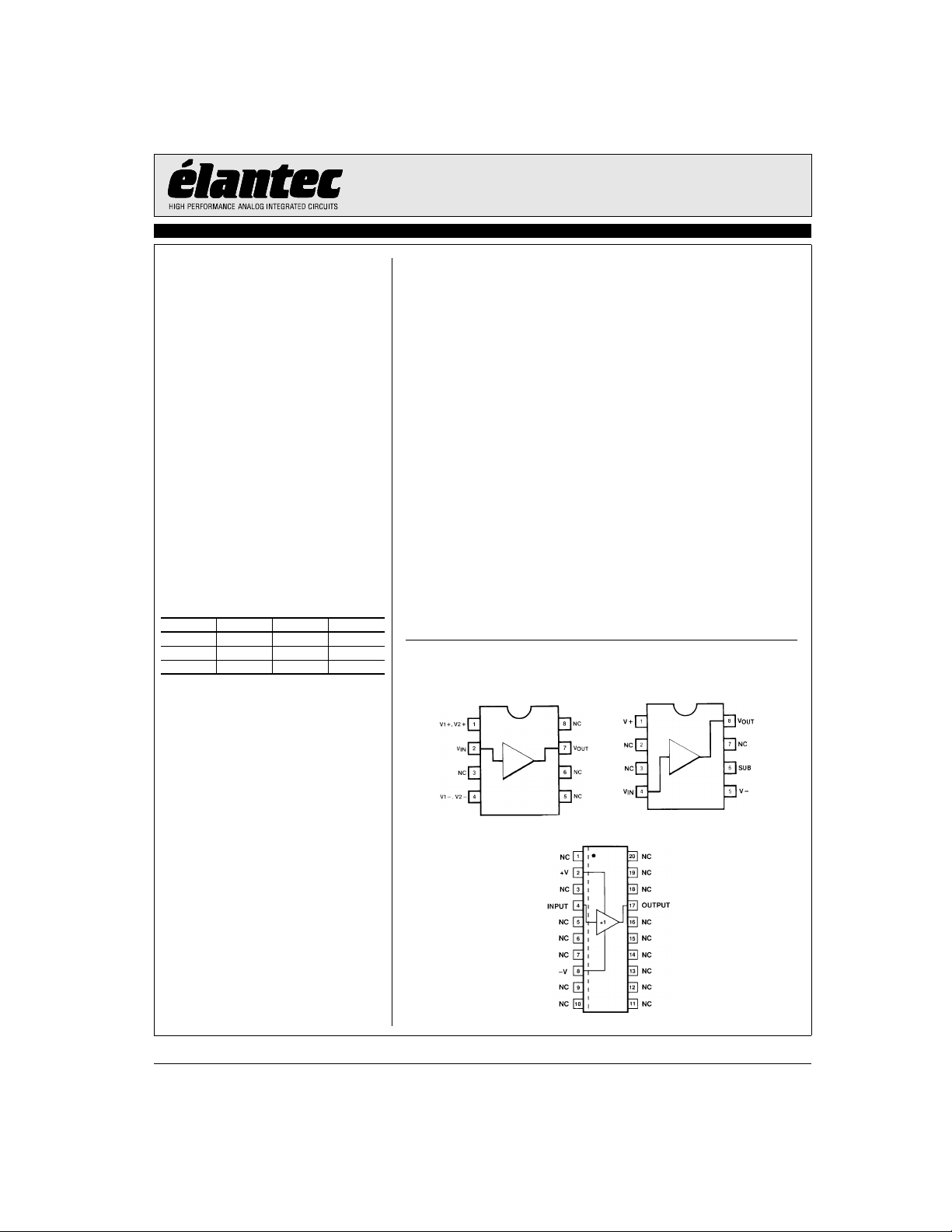
Connection Diagrams
EL2003CN EL2033CN
EL2003CM
Note: All information contained in this data sheet has been carefully checked and is believed to be accurate as of the date of publication; however, this data sheet cannot be a “controlled document”. Current revisions, if any, to these
specifications are maintained at the factory and are available upon your request. We recommend checking the revision level before finalization of your design documentation.
© 2001 Elantec Semiconductor, Inc.
September 1998, Rev F
Page 2
EL2003C, EL2033C
100MHz Video Line Driver
Absolute Maximum Ratings (T
VSSupply Voltage (V+ - V-) ±18V or 36V
VINInput Voltage ±15V or V
EL2003C, EL2033C
If the input exceeds the ratings shown (or the supplies) or if the input to output voltage
exceeds ±7.5V then the input current must be limited to ±50 mA. See the application
hints for more information.
IINInput Current (See note above) ±50mA
PDPower Dissipation See Curves
The maximum power dissipation depends on package type, ambient temperature and
heat sinking. See the characteristic curves for more details.
= 25°C)
A
Output Short Circuit Duration Continuous
A heat sink is required to keep the junction temperature below the absolute maximum
S
when the output is short circuited.
TAOperating Temperature Range EL2003C/EL2033C -40°C to +85°C
TJOperating Junction Temperature
Metal Can 175°C
Plastic 150°C
TSTStorage Temperature -65°C to +150°C
Important Note:
All parameters having Min/Max specifications are guaranteed. Typ values are for information purposes only. Unless otherwise noted, all tests are at the
specified temperature and are pulsed tests, therefore: TJ = TC = TA.
Electrical Characteristics
VS = ±15V, R
Parameter Description
V
OS
I
IN
R
IN
A
V1
A
V2
A
V3
V
01
V
02
R
OUT
I
OUT
I
S
PSRR Supply Rejection
= 50Ω
S
Test Conditions Limits
IN
Load Temp Min Typ Max
Output Offset Voltage 0 × 25°C -40 5 40 mV
T
Input Current 0 × 25°C, T
MIN
T
Input Resistance ±12V 100Ω 25°C, T
T
, T
MIN
MIN
MAX
MAX
MAX
-50 50 mV
-25 -5 25 µA
-50 50 µA
0.5 2 MΩ
0.05 MΩ
Voltage Gain ±12V 1kΩ 25°C 0.98 0.99 V/V
T
MIN
, T
MAX
0.97 V/V
Voltage Gain ±6V 50Ω 25°C 0.83 0.90 V/V
T
Voltage Gain with V
, T
MIN
= ±5V ±3V 50Ω 25°C 0.82 0.89 V/V
S
MAX
T
, T
MIN
MAX
0.80 V/V
0.79 V/V
Output Voltage Swing ±14V 1kΩ 25°C ±13 ±13.5 V
T
MIN
, T
MAX
±12.5 V
Output Voltage Swing ±12V 100Ω 25°C ±10.5 ±11.3 V
T
MIN
, T
MAX
±10 V
Output Resistance ±2V 50Ω 25°C 7 10 Ω
T
Output Current ±12V
[1]
MIN
25°C ±105 ±230 mA
T
MIN
Supply Current 0 × 25°C, T
[2]
0 × 25°C 60 80 dB
T
T
MIN
, T
, T
MIN
, T
MAX
MAX
MAX
MAX
±100 mA
10 15 mA
50 dB
12 Ω
20 mA
UnitV
2
Page 3
EL2003C, EL2033C
100MHz Video Line Driver
Electrical Characteristics
VS = ±15V, R
Parameter Description
SR1 Slew Rate
SR2 Slew Rate
THD Distortion @ 1kHz 4 V
1. Force the input to +12V and the output to +10V and measure the output current. Repeat with -12V in and -10V on the output.
2. VS = ±4.5V to ±18V.
3. Slew rate is measured between V
4. Slew rate is measured between V
= 50Ω
S
Test Conditions Limits
[3]
[4]
= +5V and -5V.
OUT
= +2.5V and -2.5V.
OUT
IN
±10V 1kΩ 25°C 600 1200 V/µs
±5V 50Ω 25°C 200 400 V/µs
RMS
Load Temp Min Typ Max
50Ω 25°C 0.2 1 %
EL2003C, EL2033C
UnitV
3
Page 4
EL2003C, EL2033C
100MHz Video Line Driver
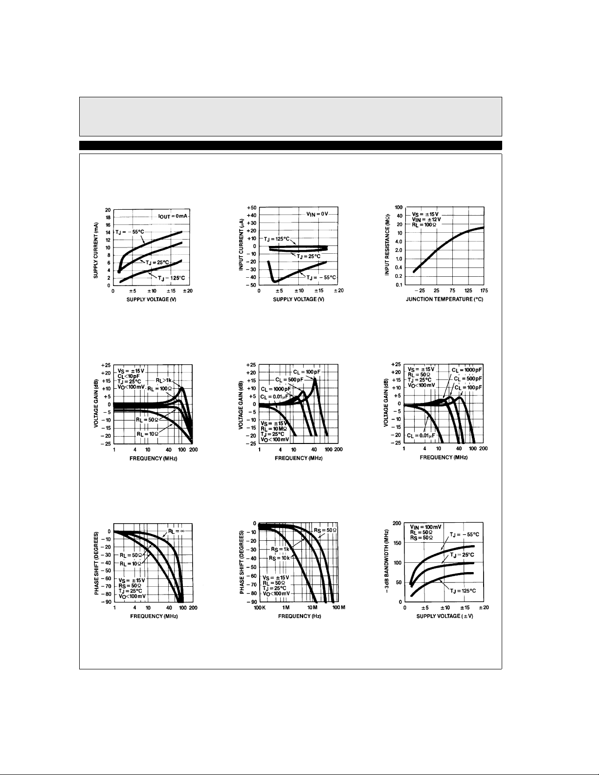
Typical Performance Curves
EL2003C, EL2033C
Quiescent Supply Current
vs Supply Voltage
Voltage Gain vs Frequency
Various Resistive Loads
Input Current
vs Supply Voltage
Voltage Gain vs Frequency
No Resistive Load
Various Capacitive Loads
3Input Resistance
vs Temperature
Voltage Gain vs Frequency
50¾ Resistive Load
Various Capacitive Loads
Phase Shift vs Frequency
Various Resistive Loads
Phase Shift vs Frequency
Various Source Resistors
4
-3 dB Bandwidth
vs Supply Voltage
Page 5
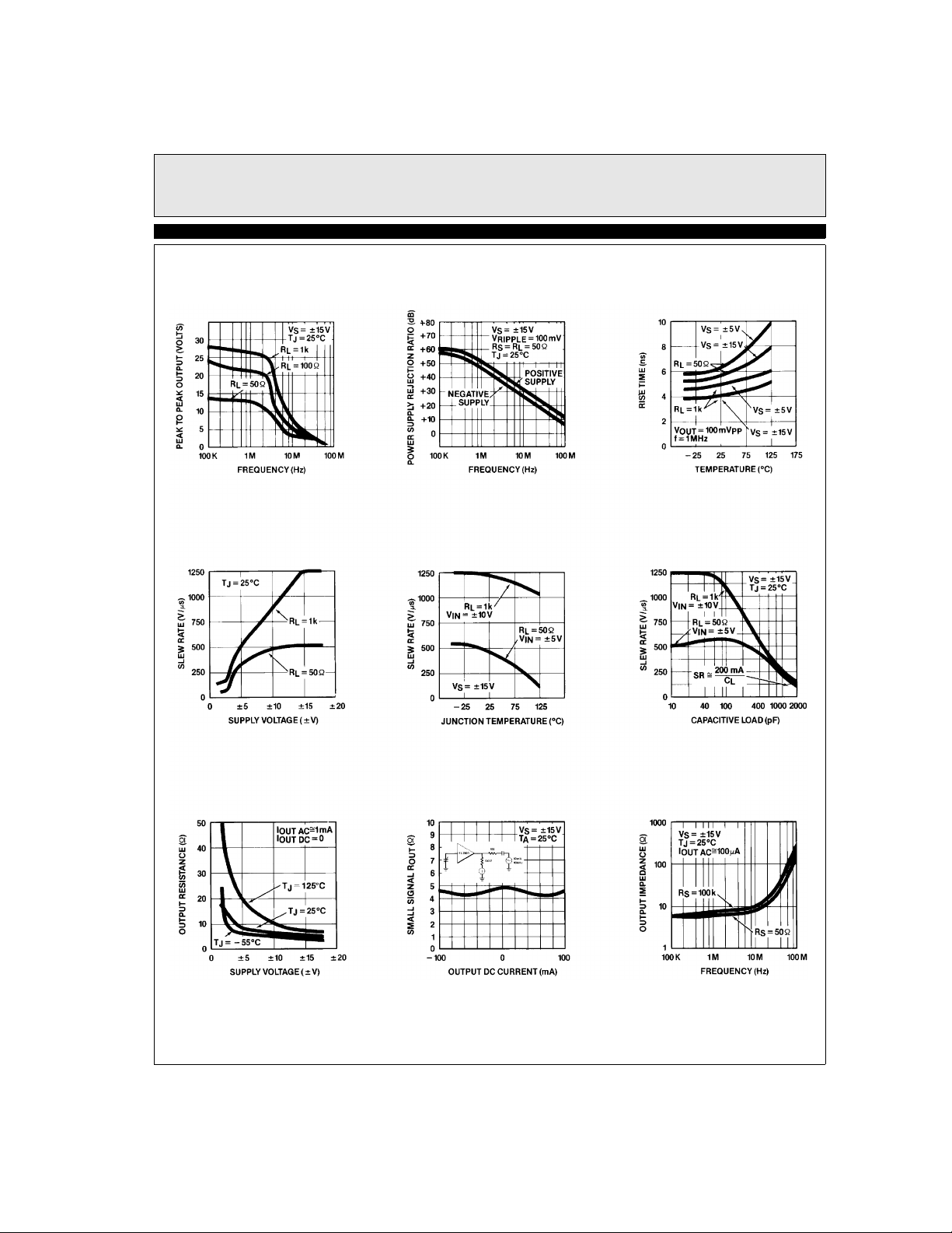
EL2003C, EL2033C
100MHz Video Line Driver
EL2003C, EL2033C
Maximum Undistorted
Output Voltage
vs Frequency
Slew Rate
vs Supply Voltage
Power Supply Rejection
Ratio vs Frequency
Slew Rate
vs Temperature
Rise Time
vs Temperature
Slew Rate
vs Capacitive Load
Output Resistance
vs Supply Voltage
Small Signal
Output Resistance
vs DC Output Current
5
Output Impedance
vs Frequency
Page 6
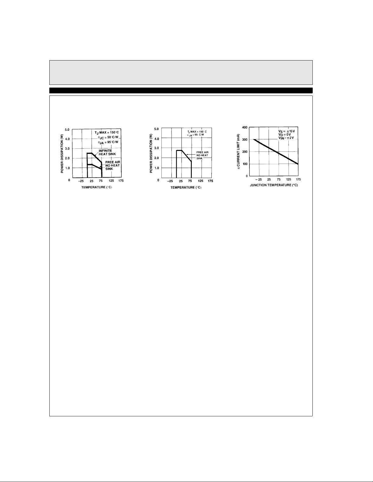
EL2003C, EL2033C
100MHz Video Line Driver
EL2003C, EL2033C
8-Lead Plastic DIP
Maximum Power Dissipation
vs Ambient Temperature
20-Lead SOL
Maximum Power Dissipation
vs Ambient Temperature
Current Limit
vs Temperature
6
Page 7

Applications Information
The EL2003C and EL2033C are monolithic buffer
amplifiers built with Elantec's proprietary dielectric isolation process that produces NPN and PNP
complimentary transistors. The circuits are connection
of symmetrical common collector transistors that provide both sink and source current capability independent
of output voltage while maintaining constant output and
input impedances. The high slew rate and wide bandwidth of the EL2003C and EL2033C make them useful
beyond video frequencies.
Power Supplies
The EL2003C and EL2033C may be operated with single or split supplies as low as ±2.5V (5V total) to as high
as ±18V (36V total). However, the bandwidth, slew rate,
and output impedance degrade significantly for supply
voltages less than ±5V (10V total) as shown in the characteristic curves. It is not necessary to use equal value
split supplies, for example -5V and +12V would be
excellent for 0V to 1V video signals.
Bypass capacitors from each supply pin to a ground
plane are recommended. The EL2003C and EL2033C
will not oscillate even with minimal bypassing, however, the supply will ring excessively with inadequate
capacitance. To eliminate a supply ringing and the interference it can cause, a 10µF tantalum capacitor with
short leads is recommended for both supplies. Inadequate supply bypassing can also result in lower slew
rates and longer settling times.
Input Range
The input to the EL2003C and EL2033C looks like a
high resistance in parallel with a few picofarads in addition to a DC bias current. The input characteristics
change very little with output loading, even when the
amplifier is in current limit. However, there are clamp
diodes from the input to the output that protect the transistor base emitter junctions. These diodes start to
conduct at about ±9.5V input to output differential voltage. Of course the input resistance drops dramatically
when the diodes start conducting; the diodes are rated at
±50mA.
The input characteristics also change when the input
voltage exceeds either supply by 0.5V. This happens
EL2003C, EL2033C
EL2003C, EL2033C
100MHz Video Line Driver
because the input transistor's base-collector junctions
forward bias. If the input exceeds the supply by LESS
than 0.5V and then returns to the normal input range, the
output will recover in less than 10ns. However, if the
input exceeds the supply by MORE than 0.5V, the
recovery time can be hundreds of nanoseconds. For this
reason it is recommended that schottky diode clamps
from input to supply be used if a fast recovery from large
input overloads is required.
Source Impedance
The EL2003C and EL2033C have excellent input-output
isolation and are very tolerant of variations in source
impedances. Capacitive sources cause no problems at
all, resistive sources up to 100kΩ present no problems as
long as care is used in board layout to minimize output
to input coupling. Inductive sources can cause oscilla-
tions; a 1kΩ resistor in series with the buffer input lead
will usually eliminate problems without sacrificing too
much speed. An unterminated cable or other resonant
source can also cause oscillations. Again, an isolating
resistor will eliminate the problem.
Current Limit
The EL2003C and EL2033C have internal current limits
that protect the output transistors. The current limit goes
down with junction temperature rise as shown in the
characteristic curves. At a junction temperature of
+175°C the current limits are at about 100mA. If the
EL2003C or EL2033C output is shorted to ground when
operating on ±15V supplies, the power dissipation will
be greater than 1.5W. A heat sink is required in order for
the EL2003C or EL2033C to survive an indefinite short.
Recovery time to come out of current limit is about
250ns.
Heat Sinking
When operating the EL2003C and EL2033C in elevated
ambient temperatures and/or high supply voltages and
low impedance loads, the internal power dissipation can
force the junction temperature above the maximum rating (150°C for the plastic DIP). Also, an indefinite short
of the output to ground will cause excessive power
dissipation.
7
Page 8

EL2003C, EL2033C
100MHz Video Line Driver
The thermal resistance junction to case is 50°C/W for
the plastic DIP. A suitable heat sink will increase the
power dissipation capability significantly beyond that of
EL2003C, EL2033C
the package alone. Several companies make standard
heat sinks for both packages. Aavid and Thermalloy heat
sinks have been used successfully.
Parallel Operation
If more than 100mA output is required or if heat management is a problem, several EL2003C or EL2033Cs
may be paralleled together. The result is as though each
device was driving only part of the load. For example, if
two units are paralleled then a 50Ω load looks like 100Ω
to each EL2003C. Parallel operation results in lower
input and output impedances, increased bias current but
no increase in offset voltage. An example showing three
EL2003Cs in parallel and also the addition of a FET
input buffer stage is shown below. By using a dual FET
the circuit complexity is minimal and the performance is
excellent. Take care to minimize the stray capacitance at
the input of the EL2003Cs for maximum slew rate and
bandwidth.
Parallel Operation
I
≥ ±300 mA
OUT
R
2Ω
OUT
BW 100MHz
SR = 1000V/µs
formed by the device output resistance and the load
resistance.
R
AV0.995
------------------------------×=
RLR
+
L
OUT
The high frequency response of the EL2003C and
EL2033C varies with the value of the load resistance as
shown in the characteristic curves. If the 100MHz peaking is undesirable when driving load resistors greater
than 50Ω, an RC snubber circuit can be used from the
output to ground. The snubber circuit works by present-
ing a high frequency load resistance of less than 50Ω
while having no loading effect at low frequencies.
Small Signal Response
RL = 50Ω, CL = 10pF, VS = ±15V
Top is VIN, Bottom is V
OUT
J1, J2 2N5911 Dual FET
R1, R2 Offset Adjust
FET Input Buffer with High Output Currents
Resistive Loads
The DC gain of the EL2003C and EL2033C is the product of the unloaded gain (0.995) and the voltage divider
Large Signal Response
RL = 100Ω, CL = 10pF, VS = ±15V
Top is VIN, Bottom is V
8
OUT
Page 9

EL2003C, EL2033C
100MHz Video Line Driver
EL2003C, EL2033C
Capacitive Loads
The EL2003C and EL2033C are stable driving any type
of capacitive load. However, when driving a pure capacitance of less than a thousand picofarads the frequency
response has excessive peaking as shown in the characteristic curves. The squarewave response will have large
overshoots and will ring for several hundred
nanoseconds.
If the peaking and ringing cause system problems they
can be eliminated with an RC snubber circuit from the
output to ground. The values can be found empirically
by observing a squarewave or the frequency response.
First just put the resistor alone from output to ground
until the desired response is obtained. Of course the gain
will be reduced due to R
series with the resistor to restore the gain at low frequencies. Start with a small capacitor and increase until the
response is optimum. Too large a capacitor will roll the
gain off prematurely and result in a longer settling time.
The figure below shows an example of an EL2003C
driving a 330pF load, which is similar to the input of a
flash converter.
. Then put capacitance in
OUT
Inductive Loads
The EL2003C and EL2033C can drive small motors,
solenoids, LDT's and other inductive loads. Foldback
current limiting is NOT used in the EL2003C or
EL2033C and current limiting into an inductive load
does NOT in and of itself cause spikes or kickbacks.
However, if the EL2003C or EL2033C is in current limit
and the input voltage is changing quickly (i.e., a squarewave) the inductive load can kick the output beyond the
supply voltage. Motors are also able to generate kickbacks when the EL2003C or EL2033C is in current
limit.
To prevent damage to the EL2003C and EL2033C when
the output kicks beyond the supplies it is recommended
that catch diodes be placed from each supply to the
output.
Reverse Isolation
The EL2003C and EL2033C have excellent output to
input isolation over a wide frequency range. This characteristic is very important when the buffer is used to
drive signals between different equipment over cables.
Often the cable is not perfect or the termination is
improper and reflections occur that act like a signal
source at the output of the buffer. Worst case the cable is
connected to a source instead of where it is supposed to
go. In both situations the buffer must keep these signals
from its input. The following curve shows the reverse
isolation of the EL2003C and EL2033C verses frequency for various source resistors.
Driving a Pure Capacitance
Top Trace is without Snubber.
Bottom Trace is with Snubber Circuit.
9
Page 10

EL2003C, EL2033C
100MHz Video Line Driver
Driving Cables
There are at least three ways to use the EL2003C and
EL2033C to drive cables, as shown in the adjacent fig-
EL2003C, EL2033C
ure. The most obvious is to directly connect the cable to
the output of the buffer. This results in a gain determined
by the output resistance of the EL2003C or EL2033C
and the characteristic impedance of the cable, assuming
it is properly terminated. For RG-58 into 50Ω the gain is
about -1dB, exclusive of cable losses. For optimum
response and minimum reflections it is important for the
cable to be properly terminated.
Double termination of a cable is the cleanest way to
drive it since reflections are absorbed on both ends of the
cable. The cable source resistor is equal to the characteristic impedance of the cable less the output resistance of
the EL2003C and EL2033C. The gain is -6dB exclusive
of the cable attenuation.
Back matching is the last and most interesting way to
drive a cable. The cable source resistor is again the characteristic impedance less the output resistance of the
EL2003C and EL2033C; the termination resistance is
now much greater than the cable impedance. The gain is
0dB and DC levels waste no power.
An additional EL2003C or EL2033C make a good
receiver at the terminating end. Because an unterminated
cable looks like a resonant circuit, the receiving
EL2003C or EL2033C should have an isolating resistor
in series with its input to prevent oscillations when the
cable is not connected to the driver. Of course if the
cable is always connected to the back match, no resistor
is necessary.
WARNING: ONE END OF A CABLE MUST BE
PROPERLY TERMINATED. If neither end is terminated in the cable characteristic impedance, the cable
will have standing waves that appear as resonances in
the frequency response. The resonant frequencies are a
function of the cable length and even relatively short
cables can cause problems at frequencies as low as
1MHz. Longer cables should be terminated on both
ends.
Direct Drive
Double Matched
Back Matched
Op Amp Booster
The EL2003C or EL2033C can boost the output drive of
almost any monolithic op amp. Because the phase shift
in the EL2003C and EL2033C is low at the op amp's
unity gain frequency, no additional compensation is
required. By following an op amp with an EL2003C or
EL2033C, the buffered op amp can drive cables and
other low impedance loads directly. Even decompensated high speed op amps can take advantage of the
EL2003C’s or EL2033C’s 100mA drive.
Op Amp Booster
Driving capacitive loads with any closed loop amplifier
creates special problems. The open loop output impedance works into the load capacitance to generate phase
lag which can make the loop unstable. The output
10
Page 11

EL2003C, EL2033C
100MHz Video Line Driver
EL2003C, EL2033C
impedance of the EL2003C or EL2033C is less than
10Ω from DC to about 10MHz, but a capacitive load of
1000pF will generate about 45° phase shift at 10MHz
and make high speed op amps unstable. Obviously more
capacitance will cause the same problem but at lower
frequencies, and slower op amps as well would become
unstable.
The easiest way to drive capacitive loads is to isolate
them from the feedback with a series resistor. Ten to
twenty ohms is usually enough but the final value
depends on the op amp used and the range of load
capacitance.
10Ω is enough isolation and speed
is determined by the isolation
resistor and capacitive load time
constant.
Op Amp Booster with Capacitive Load
C
L
10pF 17ns 10%
470pF 20ns 50%
0.001µF 30ns 35%
0.005µF 80ns 0
0.01µF 220ns 0
0.05µF 1.1µs 0
0.1µF 2.2µs 0
t
r
OS
If the system requirements will not tolerate the isolation
resistor, then additional high frequency feedback from
the op amp output (the buffer input) and an isolating
resistor from the buffer output is required. This requires
that the op amp be unity gain stable.
Complex Feedback with the Buffer to Drive Capacitive Loads
This works with any unity gain stable OA.
Snubber Circuit (51Ω 470 pF) is optional.
11
Page 12

EL2003C, EL2033C
1
100MHz Video Line Driver
Typical Applications
EL2003C, EL2033C
Butterworth
Low Pass Filter
-3dB @ 1MHz
Butterworth
High Pass Filter
-3dB @ 1MHz
Turbo Amplifier, BW = 30 MHz for Gains from 1 to 5
High Q Notch Filter
------------------------------------------
f
= 4.4MHz≈
O
2π 100pF()360()
Simulated Inductor
12
Page 13

EL2003C, EL2033C
100MHz Video Line Driver
EL2003C, EL2033C
Video Distribution Amplifier
In this broadcast quality circuit, the EL2006C FET input
amplifier provides a very high input impedance so that it
may be used with a wide variety of signal sources
including video DACs, CCD cameras, video switches or
75Ω cables. The EL2006C provides a voltage gain of 2.5
while the potentiometer allows the overall gain to be
Video Distribution Amplifier
adjusted to drive the standard signal levels into the back
matched 75Ω cables. Back matching prevents multiple
reflections in the event that the remote end of the cable is
not properly terminated. The 1k pull up resistors reduce
the differential gain error from 0.15% to less than 0.1%.
13
Page 14

EL2003C, EL2033C
100MHz Video Line Driver
Burn-In Circuits
EL2003C, EL2033C
Simplified Schematic
EL2003 DIP
EL2033 DIP
14
Page 15

EL2003C Macromodel
* Connections: +input
* | +Vsupply
* | | -Vsupply
* | | | output
* | | | |
.subckt M2003 2 1 4 7
* Input Stage
e1 10 0 2 0 1.0
r1 10 0 1K
rh 10 11 150
ch 11 0 10pF
rc 11 12 100
cc 12 0 3pF
e2 13 0 12 0 1.0
* Output Stage
q1 4 13 14 qp
q2 1 13 15 qn
q3 1 14 16 qn
q4 4 15 19 qp
r2 16 7 5
r3 19 7 5
c1 14 0 3pF
c2 15 0 3pF
i1 1 14 3mA
i2 15 4 3mA
* Bias Current
iin+ 2 0 5uA
* Models
.model qn npn(is=5e-15 bf=150 rb=350 ptf=45 cjc=2pF tf=0.3nS)
.model qp pnp(is=5e-15 bf=150 rb=350 ptf=45 cjc=2pF tf=0.3nS)
.ends
EL2003C, EL2033C
EL2003C, EL2033C
100MHz Video Line Driver
15
Page 16

EL2003C, EL2033C
100MHz Video Line Driver
EL2003C Macromodel
EL2003C, EL2033C
16
Page 17

EL2003C, EL2033C
100MHz Video Line Driver
EL2003C, EL2033C
General Disclaimer
Specifications contained in this data sheet are in effect as of the publication date shown. Elantec, Inc. reserves the right to make changes in the circuitry or specifications contained herein at any time without notice. Elantec, Inc. assumes no responsibility for the use of any circuits described
herein and makes no representations that they are free from patent infringement.
WARNING - Life Support Policy
Elantec, Inc. products are not authorized for and should not be used
within Life Support Systems without the specific written consent of
Elantec, Inc. Life Support systems are equipment intended to sup-
Elantec Semiconductor, Inc.
675 Trade Zone Blvd.
Milpitas, CA 95035
Telephone: (408) 945-1323
(888) ELANTEC
Fax: (408) 945-9305
European Office: +44-118-977-6020
Japan Technical Center: +81-45-682-5820
port or sustain life and whose failure to perform when properly used
in accordance with instructions provided can be reasonably
expected to result in significant personal injury or death. Users contemplating application of Elantec, Inc. Products in Life Support
Systems are requested to contact Elantec, Inc. factory headquarters
to establish suitable terms & conditions for these applications. Elantec, Inc.’s warranty is limited to replacement of defective
components and does not cover injury to persons or property or
other consequential damages.
September 1998, Rev F
17
Printed in U.S.A.
 Loading...