

Page 1
EL2001C
Low Power, 70 MHz Buffer Amplifier
EL2001C December 1995 Rev G
Features
# 1.3 mA supply current
# 70 MHz bandwidth
# 2000 V/ms slew rate
# Low bias current, 1 mA typical
# 100 mA output current
# Short circuit protected
# Low cost
# Stable with capacitive loads
# Wide supply range
g
5V tog15V
# No thermal runaway
Applications
# Op amp output current booster
# Cable/line driver
# A/D input buffer
# Low standby current systems
Ordering Information
Part No. Temp. Range Pkg. Outline
EL2001ACN 0§Ctoa75§C P-DIP MDP0031
EL2001CM 0§Ctoa75§C 20-Lead SOL MDP0027
EL2001CN 0§Ctoa75§C P-DIP MDP0031
General Description
The EL2001 is a low cost monolithic, high slew rate, buffer
amplifier. Built using the Elantec monolithic Complementary
Bipolar process, this patented buffer has a
b
3 dB bandwidth of
70 MHz, and delivers 100 mA, yet draws only 1.3 mA of supply
current. It typically operates from
will work with as little as
g
5V.
g
15V power supplies but
This high speed buffer may be used in a wide variety of applications in military, video and medical systems. A typical example
is a general purpose op amp output current booster where the
buffer must have sufficiently high bandwidth and low phase
shift at the maximum frequency of the op amp.
Elantec’s products and facilities comply with MIL-I-45208A,
and other applicable quality specifications. For information on
Elantec’s processing, see the Elantec document, QRA-1: Elan-
tec’s Processing, Monolithic Integrated Circuits.
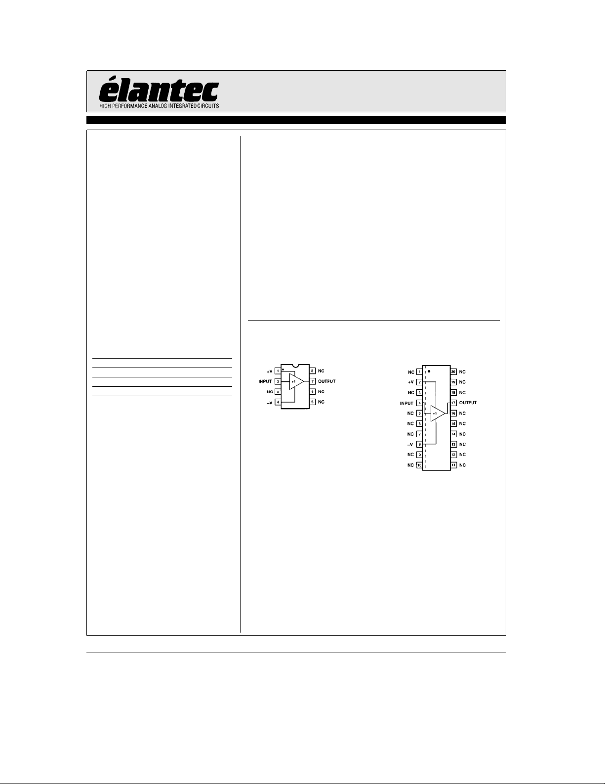
Connection Diagrams
Ý
EL2001 DIP Pinout EL2001 SOL Pinout
2001– 1
Top View
Top View
Note: Non-designated pins are no connects and are not electrically connected
internally.
Manufactured under U.S. Patent No. 4,833,424, 4,827,223 U.K. Patent No.
2217134
Note: All information contained in this data sheet has been carefully checked and is believed to be accurate as of the date of publication; however, this data sheet cannot be a ‘‘controlled document’’. Current revisions, if any, to these
specifications are maintained at the factory and are available upon your request. We recommend checking the revision level before finalization of your design documentation.
©
1989 Elantec, Inc.
2001– 2
Page 2
EL2001C
Low Power, 70 MHz Buffer Amplifier
Absolute Maximum Ratings
V
S
V
IN
I
IN
P
D
Supply Voltage (VabVb)
Input Voltage (Note 1)
Input Current (Note 1)
Power Dissipation (Note 2) See Curves
Output Short Circuit
g
18V or 36V
g
15V or V
g
50 mA
Duration (Note 3) Continuous
Important Note:
All parameters having Min/Max specifications are guaranteed. The Test Level column indicates the specific device testing actually
performed during production and Quality inspection. Elantec performs most electrical tests using modern high-speed automatic test
equipment, specifically the LTX77 Series system. Unless otherwise noted, all tests are pulsed tests, therefore T
Test Level Test Procedure
I 100% production tested and QA sample tested per QA test plan QCX0002.
II 100% production tested at T
III QA sample tested per QA test plan QCX0002.
IV Parameter is guaranteed (but not tested) by Design and Characterization Data.
V Parameter is typical value at T
T
MAX
and T
per QA test plan QCX0002.
MIN
e
25§C and QA sample tested at T
A
e
25§C for information purposes only.
A
T
Operating Temperature Range
A
S
EL2001AC/EL2001C 0
T
Operating Junction Temperature 150§C
J
T
Storage Temperature
ST
J
e
25§C,
A
Ctoa75§C
§
b
65§Ctoa150§C
e
e
T
TA.
C
Electrical Characteristics
Parameter Description
V
OS
I
IN
R
IN
Offset Voltage
EL2001A/EL2001AC
EL2001/EL2001C
Input Current
EL2001A/EL2001AC
EL2001/EL2001C
Input Resistance
e
g
V
S
15V, R
e
50X, unless otherwise specified
S
Test Conditions Limits
V
Load Temp Min Typ Max
IN
25
C
0
0
0
0
g
12V 100X
%
%
%
%
§
T
MIN,TMAX
25
C
§
T
MIN,TMAX
25
C
§
T
MIN,TMAX
25
C
§
T
MIN,TMAX
25
§
T
MIN,TMAX
EL2001AC
EL2001C
Units
Test
Level
b
10 2 I I mV
b
15
b
30 2
b
40
b
31
b
6
b
51
b
10
a
15 III mV
a
30 I mV
a
40 III mV
a
3I mA
a
6 III mA
a
5I mA
a
10 III mA
18 I MX
0.5 III MX
TDis 2.5in
2
Page 3
EL2001C
Low Power, 70 MHz Buffer Amplifier
Electrical Characteristics
Parameter Description
A
V1
A
V2
A
V3
V
O
R
OUT
I
OUT
I
S
PSRR Supply Rejection,
t
r
t
d
Voltage Gain
Voltage Gain
Voltage Gain
e
with V
g
S
Output Voltage
Swing
Output Resistance
Output Current
5V
g
g
g
g
g
g
Supply Current
(Note 5)
Rise Time 0.5V 100X 25§C 4.2 V ns
Propagation Delay 0.5V 100X 25§C 2.0 V ns
e
g
V
S
Test Conditions Limits
V
Load Temp Min Typ Max
in
12V
%
10V 100X
3V 100X
12V 100X
2V 100X
12V (Note 4)
0
0
%
%
e
15V, R
50X, unless otherwise specified Ð Contd.
S
T
MIN,TMAX
T
MIN,TMAX
T
MIN,TMAX
T
MIN,TMAX
T
MIN,TMAX
T
MIN,TMAX
T
MIN,TMAX
T
MIN,TMAX
EL2001AC
EL2001C
Units
Test
Level
25
C 0.990 0.998 I V/V
§
0.985 III V/V
C 0.83 0.93 I V/V
25
§
0.80 III V/V
C 0.82 0.89 I V/V
25
§
0.79 III V/V
C
25
§
C1015IX
25
§
g
g
g
10
11 I V
9.5 III V
18 III X
C
25
§
25
C 1.3 2.0 I mA
§
g
100g160 I mA
g
95 III mA
2.5 III mA
25
C6075 I dB
§
50 III dB
SR Slew Rate, (Note 6)g10V 100X 25§C 1200 2000 IV V/ms
Note 1: If the input exceeds the ratings shown (or the supplies) or if the input to output voltage exceedsg7.5V then the input
current must be limited to
Note 2: The maximum power dissipation depends on package type, ambient temperature and heat sinking. See the characteristic
curves for more details.
g
50 mA. See the applications section for more information.
Note 3: A heat sink is required to keep the junction temperature below the absolute maximum when the output is short circuited.
a
Note 4: Force the input to
output.
Note 5: V
is measured at V
OS
simultaneously.
Note 6: Slew rate is measured between V
12V and the output toa10V and measure the output current. Repeat withb12 VINandb10V on the
aea
S
4.5V, V
OUT
beb
S
ea
5V andb5V.
4.5V and at V
aea
S
18V, V
beb
S
18V. Both supplies are changed
TDis 4.2in
3
Page 4
EL2001C
Low Power, 70 MHz Buffer Amplifier
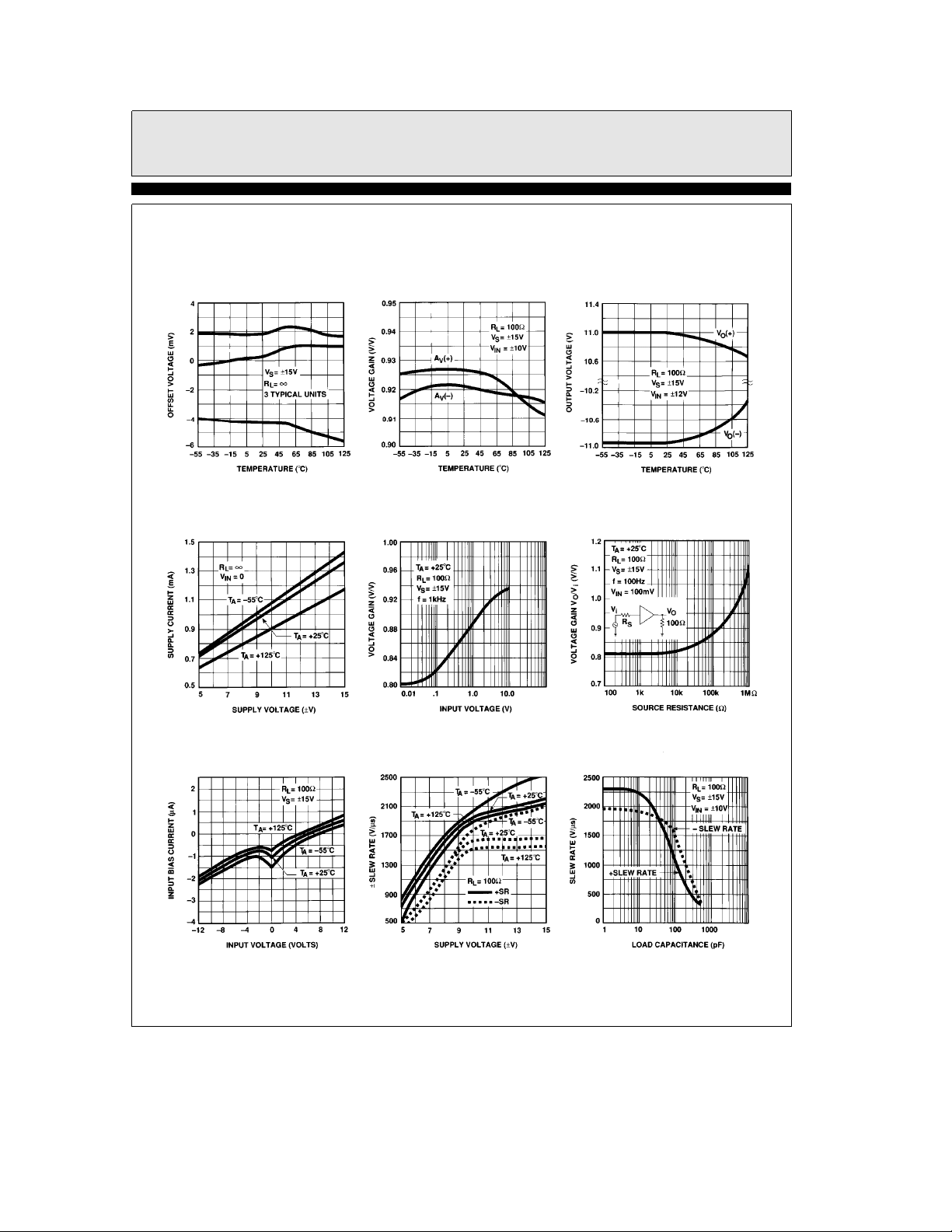
Typical Performance Curves
Offset Voltage
vs Temperature
Supply Current
vs Supply Voltage
Voltage Gain
vs Temperature
Voltage Gain
vs Input Voltage
Output Voltage Swing
vs Temperature
Voltage Gain
vs Source Resistance
Input Bias Current
vs Input Voltage
g
Slew Rate
vs Supply Voltage
4
g
Slew Rate
vs Capacitive Load
2001– 4
Page 5

EL2001C
Low Power, 70 MHz Buffer Amplifier
Typical Performance Curves
Voltage Gain vs Frequency
for Various Resistive Loads
Phase Shift vs Frequency
for Various Capacitive Loads
Ð Contd.
Voltage Gain
vs Frequency for Various
Capacitive Loads; R
b
3 dB Bandwidth
vs Supply Voltage
e
L
100X
Voltage Gain
vs Frequency for Various
Capacitive Loads; R
Power Supply Rejection Ratio
vs Frequency
L
e %
Output Impedance vs Frequency Reverse Isolation vs Frequency vs Output Current
Small Signal Output Resistance
5
2001– 5
Page 6

EL2001C
Low Power, 70 MHz Buffer Amplifier
Typical Performance Curves
8-Lead Plastic DIP
Maximum Power Dissipation
vs Ambient Temperature
Large Signal Response
Ð Contd.
20-Lead SOL
Maximum Power Dissipation
vs Ambient Temperature
Small Signal Response
2001– 7
Short Circuit Current
vs Temperature
2001– 6
2001– 8
6
Page 7

EL2001C
Low Power, 70 MHz Buffer Amplifier
Burn-In Circuit
2001– 9
Simplified Schematic
2001– 10
Application Information
The EL2001 is a monolithic buffer amplifier built
on Elantec’s proprietary dielectric isolation process that produces NPN and PNP transistors
with essentially identical DC and AC characteristics. The EL2001 takes full advantage of the complementary process with a unique circuit topology.
Elantec has applied for two patents based on the
EL2001’s topology. The patents relate to the base
drive and feedback mechanism in the buffer. This
feedback makes 2000 V/ms slew rates with 100X
loads possible with very low supply current.
Power Supplies
The EL2001 may be operated with single or split
supplies with total voltage difference between
g
10V (
to use equal split value supplies. For example
b
from
Bypass capacitors from each supply pin to
ground are highly recommended to reduce supply
ringing and the interference it can cause. At a
minimum, 1 mF tantalum capacitor with short
leads should be used for both supplies.
5V) and 36V (g18V). It is not necessary
5V anda12V would be excellent for signals
b
2V toa9V.
Input Characteristics
The input to the EL2001 looks like a resistance in
parallel with about 3.5 picofarads in addition to a
DC bias current. The DC bias current is due to
the miss-match in beta and collector current between the NPN and PNP transistors connected
to the input pin. The bias current can be either
positive or negative. The change in input current
with input voltage (R
put load, beta and the internal boost. R
actually appear negative over portions of the input range; typical input current curves are shown
in the characteristic curves. Internal clamp diodes from the input to the output are provided.
These diodes protect the transistor base emitter
junctions and limit the boost current during slew
to avoid saturation of internal transistors. The
diodes begin conduction at about
output differential. When that happens the input
resistance drops dramatically. The diodes are rated at 50 mA. When conducting they have a series
resistance of about 20X. There is also 100 X in
series with the input that limits input current.
g
Above
tional series resistance should be added.
7.5V differential input to output, addi-
) is affected by the out-
IN
g
IN
2.5V input to
can
Source Impedance
The EL2001 has good input to output isolation.
When the buffer is not used in a feedback loop,
capactive and resistive sources up to 1 Meg present no oscillation problems. Care must be used in
board layout to minimize output to input coupling. CAUTION: When using high source impedances (R
can be observed due to output offset, load resistor, and the action of the boost circuit. See typical performance curves.
l
100 kX), significant gain errors
S
7
Page 8

EL2001C
Low Power, 70 MHz Buffer Amplifier
EL2001C Macromodel
*Connections:ainput
*
*
*
*
.subckt M2001 2 1 4 7
* Input Stage
el100201.0
r1 10 0 1K
rh 10 11 150
ch 11 0 9pF
rc 11 12 100
cc 12 0 4pF
e2 13 0 12 0 1.0
* Output stage
q141314qp
q211315qn
q311416qn
q441519qp
r2 16 7 1
r3 19 7 1
i1 1 14 0.9mA
i2 15 4 0.9mA
* Bias Current
a
iin
2 0 1uA
* Models
.model qn npn(is
.model qp pnp(is
.ends
a
Vsupply
l
ll
lll
b
Vsupply
output
llll
e5eb
15 bfe150 rbe200 ptfe45 tfe0.1nS)
e5eb
15 bfe150 rbe200 ptfe45 tfe0.1nS)
TABWIDE
TDis 3.9in
8
Page 9

EL2001C
Low Power, 70 MHz Buffer Amplifier
EL2001C Macromodel
Ð Contd.
2001– 11
9
Page 10

BLANK
10
Page 11

BLANK
11
Page 12

EL2001C
Low Power, 70 MHz Buffer Amplifier
EL2001CDecember 1995 Rev G
General Disclaimer
Specifications contained in this data sheet are in effect as of the publication date shown. Elantec, Inc. reserves the right to make changes
in the circuitry or specifications contained herein at any time without notice. Elantec, Inc. assumes no responsibility for the use of any
circuits described herein and makes no representations that they are free from patent infringement.
WARNING Ð Life Support Policy
Elantec, Inc. products are not authorized for and should not be
used within Life Support Systems without the specific written
consent of Elantec, Inc. Life Support systems are equipment in-
Elantec, Inc.
1996 Tarob Court
Milpitas, CA 95035
Telephone: (408) 945-1323
(800) 333-6314
Fax: (408) 945-9305
European Office: 44-71-482-4596
tended to support or sustain life and whose failure to perform
when properly used in accordance with instructions provided can
be reasonably expected to result in significant personal injury or
death. Users contemplating application of Elantec, Inc. products
in Life Support Systems are requested to contact Elantec, Inc.
factory headquarters to establish suitable terms & conditions for
these applications. Elantec, Inc.’s warranty is limited to replacement of defective components and does not cover injury to persons or property or other consequential damages.
Printed in U.S.A.12
 Loading...