

Page 1
EL1881C
Sync Separator, Low Power
EL1881C
Features
• NTSC, PAL, SECAM, non-
standard video sync separation
• Fixed 70mV slicing of video input
levels from 0.5V
P-P
to 2V
P-P
• Low supply current - 1.5mA typ.
• Single +5V supply
• Composite, vertical sync output
• Odd/even field output
• Burst/back porch output
• Available in 8-pin PDIP and SO
packages
Applications
• Video amplifiers
• PCMCIA applications
• A/D drivers
• Line drivers
• Portable computers
• High-speed communications
• RGB applications
• Broadcast equipment
• Active filtering
General Description
The EL1881C video sync separator is manufactured using Elantec’s
high performance analog CMOS process. This device extracts sync
timing information from both standard and non-standard video input.
It provides composite sync, vertical sync, burst/back porch timing, and
odd/even field detection. Fixed 70mV sync tip slicing provides sync
edge detection when the video input level is between 0.5V
2V
(sync tip amplitude 143mV to 572mV). A single external resis-
P-P
P-P
and -
tor sets all internal timing to adjust for various video standards. The
composite sync output follows video in sync pulses and a vertical sync
pulse is output on the rising edge of the first vertical serration following the vertical pre-equalizing string. For non-standard vertical inputs,
a default vertical pulse is output when the vertical signal stays low for
longer than the vertical sync default delay time. The odd/even output
indicates field polarity detected during the vertical blanking interval.
The EL1881C is plug-in compatible with the industry-standard
LM1881 and can be substituted for that part in 5V applications with
lower required supply current.
The EL1881C is available in the 8-pin PDIP and SO packages and is
specified for operation over the full -40°C to +85°C temperature
range.
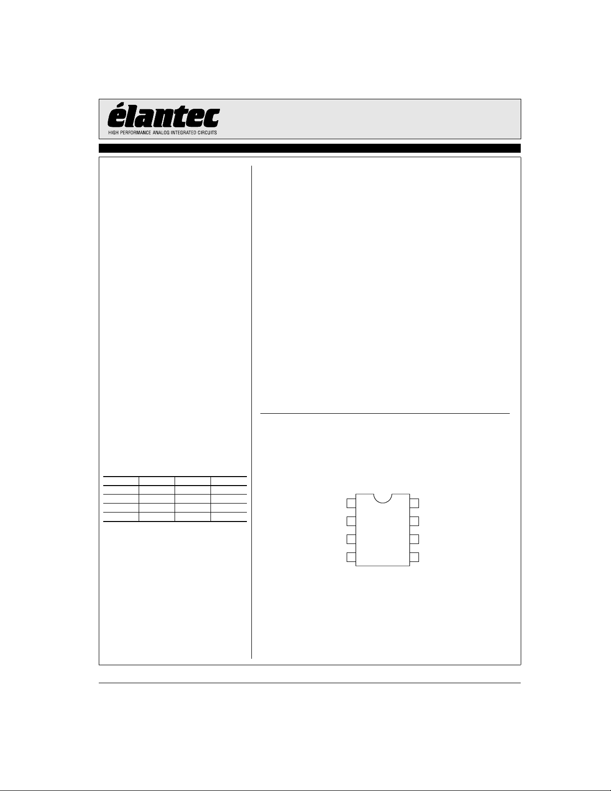
Connection Diagram
Ordering Information
Part No. Package Tape & Reel Outline #
EL1881CN 8-Pin PDIP - MDP0031
EL1881CS 8-Pin SO - MDP0027
EL1881CS-T7 8-Pin SO 7” MDP0027
EL1881CS-T13 8-Pin SO 13” MDP0027
Demo Board
Composite Sync Out
Composite Video In
Vertical Sync Out
A dedicated demo board is available.
Note: All information contained in this data sheet has been carefully checked and is believed to be accurate as of the date of publication; however, this data sheet cannot be a “controlled document”. Current revisions, if any, to these
specifications are maintained at the factory and are available upon your request. We recommend checking the revision level before finalization of your design documentation.
© 2001 Elantec Semiconductor, Inc.
GND
1
2
3
4
8
VDD 5V
7
Odd/Even Output
6
RSET
5
Burst/Back Porch Output
September 18, 2001
Page 2
EL1881C
Sync Separator, Low Power
EL1881C
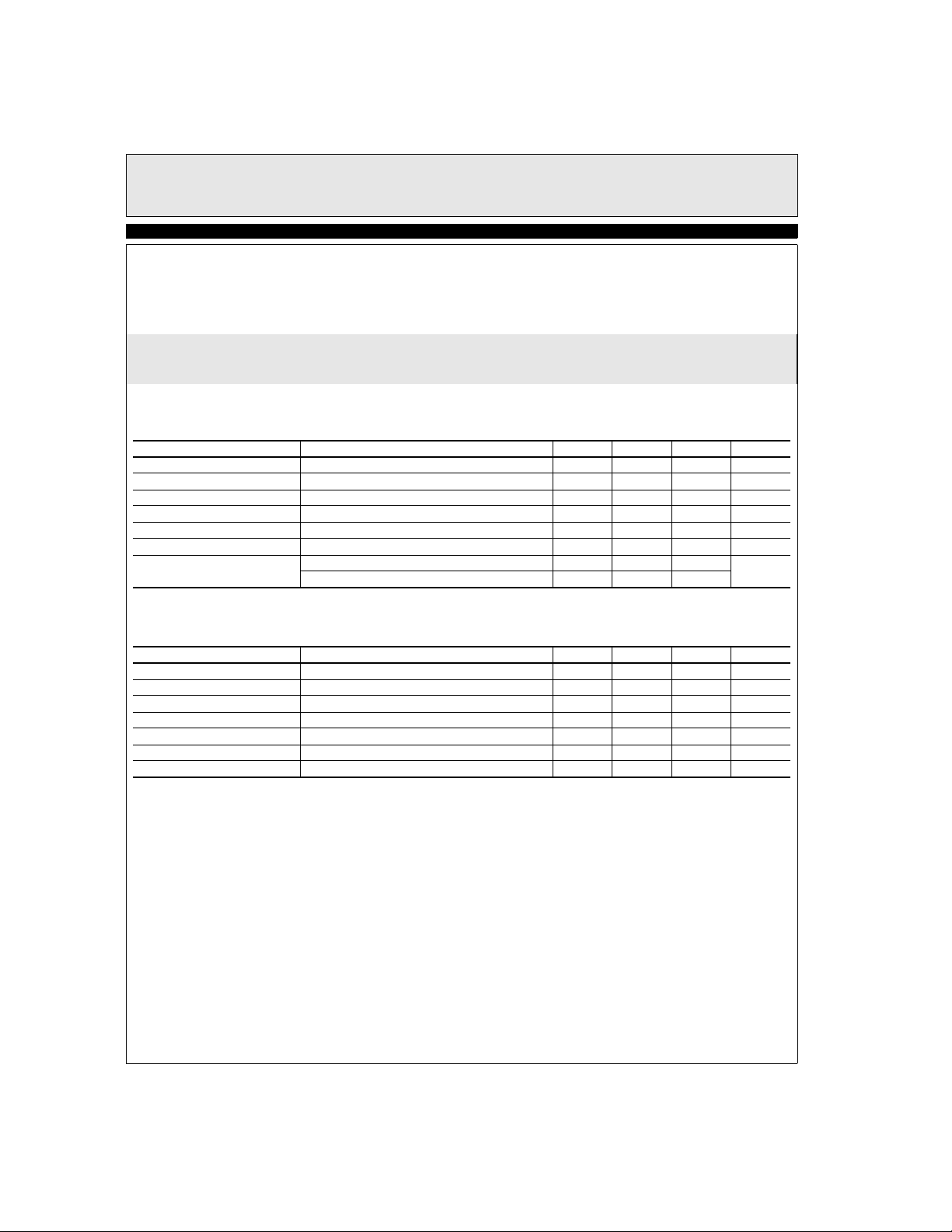
Absolute Maximum Ratings (T
VCC Supply 7V
Storage Temperature -65°C to +150°C
Pin Voltages -0.5V to V
Important Note:
All parameters having Min/Max specifications are guaranteed. Typ values are for information purposes only. Unless otherwise noted, all tests are at the
specified temperature and are pulsed tests, therefore: TJ = TC = TA.
= 25°C)
A
CC
+0.5V
Operating Ambient Temperature Range -40°C to +85°C
Operating Junction Temperature 150°C
Power Dissipation 400mW
DC Characteristics
V
= 5V, TA = 25°C, R
DD
Parameter Description Min Typ Max Unit
IDD, Quiescent VDD = 5V 0.75 1.5 3 mA
Clamp Voltage Pin 2, I
Clamp Discharge Current Pin 2 = 2V 6 12 16 µA
Clamp Charge Current Pin 2 = 1V -1.3 -1 0.7 mA
R
Pin Reference Voltage Pin 6 1.1 1.22 1.35 V
SET
VOL Output Low Voltage IOL = 1.6mA 0.24 0.5 V
VOH Output High Voltage
= 681kΩ, unless otherwise specified.
SET
= -100µA 1.35 1.5 1.65 V
LOAD
IOH = -40µA 4 4.8
IOH = -1.6mA 3 4.6
V
Dynamic Characteristics
Parameter Description Min Typ Max Unit
Comp Sync Prop Delay, t
Vertical Sync Width, t
Vertical Sync Default Delay, t
Burst/Back Porch Delay, t
Burst/Back Porch Width, t
Input Dynamic Range Video Input Amplitude to Maintain 50% Slice Spec 0.5 2 V
Slice Level V
CS
VS
BD
B
See Figure 2 20 35 75 ns
Normal or Default Trigger, 50%-50% 190 230 300 µs
See Figure 3 35 62 85 µs
VSD
See Figure 2 120 200 300 ns
See Figure 2 2.5 3.5 4.5 µs
SLICE/VCLAMP
55 70 85 mV
P-P
2
Page 3
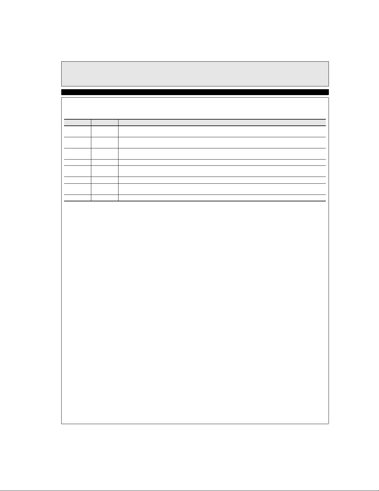
Pin Descriptions
Pin Number Pin Name Pin Function
1 Composite
2 Composite
3 Vertical Sync
4 GND Supply ground
5 Burst/Back
6 R
7 Odd/Even
8 VDD 5V Positive supply (5V)
1. R
SET
Sync Out
Video In
Porch Output
SET
Output
must be a 1% resistor
Composite sync pulse output; sync pulses start on a falling edge and end on a rising edge
AC coupled composite video input; sync tip must be at the lowest potential (positive picture phase)
Vertical sync pulse output; the falling edge of vert sync is the start of the vertical period
Out
Burst/back porch output; low during burst portion of composite video
[1]
An external resistor to ground sets all internal timing; a 681k 1% resistor will provide correct timing for NTSC signals
Odd/even field output; high during odd fields, low during even fields; transitions occur at start of vert sync pulse
EL1881C
EL1881C
Sync Separator, Low Power
3
Page 4
EL1881C
Sync Separator, Low Power
EL1881C
Typical Performance Curves
Supply Current vs Temperature
R
=681kΩ
SET
1.65
1.6
1.55
1.5
1.45
Supply Current (mA)
1.4
1.35
-50 -25 25 75 100
Clamp Discharge Current vs Temperature
R
SET
11.4
11.3
11.2
11.1
11
10.9
Clamp Discharge Current (µA)
10.8
10.7
5.5V
5V
4.5V
0 50 -50 -25 25 75 1000 50
Temperature (°C)
=681kΩ
5.5V
5V
4.5V
Temperature (°C)
V
Voltage vs Temperature
CLAMP
R
=681kΩ
SET
1.535
1.525
1.515
(V)
CLAMP
V
1.505
1.495
1.485
V
vs Temperature
RSET
R
=681kΩ
SET
1.24
1.235
1.23
1.225
(V)
1.22
RSET
V
1.215
1.21
1.205
1.2
-50 -25 25 75 1000 50-50 -25 25 75 1000 50
5.5V
5V
4.5V
Temperature (°C)
5.5V
5V
4.5V
Temperature (°C)
Clamp Charge Current vs Temperature
R
=681kΩ
SET
1.1
1.05
1
0.95
Clamp Charge Current (mA)
0.9
0.85
5V
-50 -25 25 75 1000 50
Temperature (°C)
5.5V
4.5V
R
vs Horizontal Frequency
SET
1000
800
600
(kΩ)
SET
R
400
200
0
10 15 25 35 40 45
20 30
Frequency (kHz)
4
Page 5

Typical Performance Curves
EL1881C
EL1881C
Sync Separator, Low Power
Burst/Back Porch Width vs R
VDD=5V, TA=25°C
6
5
4
3
Burst Width (µS)
2
1
200 400 600 800 1000
Vertical Sync Width vs R
VDD=5V, TA=25°C
350
300
250
200
150
100
Vertical Sync Width (µS)
50
0
200 400 600 1000
SET
R
(kΩ)
SET
SET
800
R
(kΩ)
SET
Burst/Back Porch Delay vs R
VDD=5V, TA=25°C
350
300
250
200
150
100
Burst/Back Porch Delay (ns)
50
0
200 400 800 1000
Vertical Default Delay vs R
VDD=5V, TA=25°C
120
100
80
60
40
Vertical Sync Default Delay (µS)
20
0
200 400 600 800 1000
SET
600
R
(kΩ)
SET
SET
R
(kΩ)
SET
Composite Sync Prop Delay vs Temperature
41
39
37
35
33
Composite Sync Prop Delay (ns)
31
-50 -25 0 50 100
25 75 -50 -25 0 50 10025 75
Temperature (°C)
Burst/Back Porch Width vs Temperature
3.9
3.8
3.7
3.6
3.5
3.4
3.3
Burst/Back Porch Width (µS)
3.2
3.1
5.5V
5V 4.5V
Temperature (°C)
5
Page 6

EL1881C
Sync Separator, Low Power
EL1881C
Typical Performance Curves
Burst/Back Porch Delay vs Temperature
R
=681kΩ
SET
250
5.5V
200
150
100
Burst/Back Porch Delay (ns)
50
0
-50 -25 0 50 100
Vertical Sync Default Delay Time vs Temperature
R
SET
64.5
63.5
62.5
61.5
60.5
Vertical Sync Default Delay Time (µS)
59.5
-50 -25 0 50 10025 75
4.5V
Temperature (°C)
=681kΩ
5.5V
5V
4.5V
Temperature (°C)
5V
25 75 0 50
Vertical Sync Pulse Width vs Temperature
R
=681kΩ
SET
239
237
235
233
Vertical Sync Pulse Width (µs)
231
229
-50 -25 25 75 100
Composite Sync to Vertical Sync Delay Time
R
=681kΩ
SET
20
18
16
(ns)
CS-VS
t
14
12
10
-50 -25 0 50 100
5.5V
5V
4.5V
Temperature (°C)
4.5V
5.5V
25 75
Temperature (°C)
5V
Composite Sync to Odd/Even Delay Time
R
=681kΩ
SET
27
25
23
(ns)
21
CS-OE
t
19
17
15
-50 -25 0 25 50 75 100
4.5V
5V
5.5V
Temperature (°C)
Package Power Dissipation vs Ambient Temp.
JEDEC JESD51-3 Low Effective Thermal Conductivity Test Board
1.4
1.2
1.25W
1
0.8
781mW
0.6
Power Dissipation (W)
0.4
0.2
0
0 25 50 75 100 125 150
P
D
Θ
I
P
J
8
A
=
1
0
0
°
C
/
W
S
O
8
Θ
J
A
=
1
6
0
°
C
/
W
Ambient Temperature (°C)
85
6
Page 7

Timing Diagrams
EL1881C
EL1881C
Sync Separator, Low Power
Notes:
b. The composite sync output reproduces all the video input sync pulses, with a propagation delay.
c. Vertical sync leading edge is coincident with the first vertical serration pulse leading edge, with a propagation delay.
d. Odd-even output is low for even field, and high for odd field.
e. Back porch goes low for a fixed pulse width on the trailing edge of video input sync pulses. Note that for serration pulses
during vertical, the back porch starts on the rising edge of the serration pulse (with propagation delay).
* Signal 1a drawing reproduced with permission from EIA.
Figure 1. Standard (NTSC Input) Timing
7
Page 8

EL1881C
Sync Separator, Low Power
EL1881C
Expanded Timing Diagrams
Figure 2. Standard Vertical Timing
Figure 3. Non-Standard Vertical Timing
8
Page 9

EL1881C
Sync Separator, Low Power
EL1881C
Figure 4. Standard (NTSC Input) H. Sync Detail
9
Page 10

EL1881C
Sync Separator, Low Power
EL1881C
Applications Information
Video In
A simplified block diagram is shown following page.
An AC coupled video signal is input to Video In pin 2
via C1, nominally 0.1µF. Clamp charge current will prevent the signal on pin 2 from going any more negative
than Sync Tip Ref, about 1.5V. This charge current is
nominally about 1mA. A clamp discharge current of
about 10µA is always attempting to discharge C1 to
Sync Tip Ref, thus charge is lost between sync pulses
that must be replaced during sync pulses. The droop
voltage that will occur can be calculated from IT = CV,
where V is the droop voltage, I is the discharge current,
T is the time between sync pulses (sync period - sync tip
width), and C is C1.
An NTSC video signal has a horizontal frequency of
15.73kHz, and a sync tip width of 4.7µs. This gives a
period of 63.6µs and a time T = 58.9µs. The droop voltage will then be V = 5.9mV. This is less than 2% of a
nominal sync tip amplitude of 286mV. The charge represented by this droop is replaced in a time given by T =
CV/I, where I = clamp charge current = 1mA. Here T =
590ns, about 12% of the sync pulse width of 4.7µs. It is
important to choose C1 large enough so that the droop
voltage does not approach the switching threshold of the
internal comparator.
Fixed Gain Buffer
The clamped video signal then passes to the fixed gain
buffer which places the sync slice level at the equivalent
level of 70mV above sync tip. The output of this buffer
is presented to the comparator, along with the slice reference. The comparator output is level shifted and
buffered to TTL levels, and sent out as Composite Sync
to pin 1.
Burst
A low-going Burst pulse follows each rising edge of
sync, and lasts approximately 3.5µs for an R
681kΩ.
SET
of
Vertical Sync
A low-going Vertical Sync pulse is output during the
start of the vertical cycle of the incoming video signal.
The vertical cycle starts with a pre-equalizing phase of
pulses with a duty cycle of about 93%, followed by a
vertical serration phase that has a duty cycle of about
15%. Vertical Sync is clocked out of the EL1881C on
the first rising edge during the vertical serration phase.
In the absence of vertical serration pulses, a vertical sync
pulse will be forced out after the vertical sync default
delay time, approximately 60µS after the last falling
edge of the vertical equalizing phase for R
= 681kΩ.
SET
Odd/Even
Because a typical television picture is composed of two
interlaced fields, there is an odd field that includes all
the odd lines, and an even field that consists of the even
lines. This odd/even field information is decoded by the
EL1881C during the end of picture information and the
beginning of vertical information. The odd/even circuit
includes a T-flip-flop that is reset during full horizontal
lines, but not during half lines or vertical equalization
pulses. The T-flip-flop is clocked during each falling
edge of these half hperiod pulses. Even fields will toggle
until a low state is clocked to the odd/even pin 7 at the
beginning of vertical sync, and odd fields will cause a
high state to be clocked to the odd/even pin at the start of
the next vertical sync pulse. Odd/even can be ignored if
using non-interlaced video, as there is no change in timing from one field to the next.
R
SET
An external R
ground, produces a reference current that is used internally as the timing reference for vertical sync width,
vertical sync default delay, burst gate delay and burst
width. Decreasing the value of R
ence current, which in turn decreases reference times
and pulse widths. A higher frequency video input necessitates a lower R
resistor, connected from R
SET
SET
value.
SET
pin 6 to
SET
increases the refer-
Chroma Filter
A chroma filter is suggested to increase the S/N ratio of
the incoming video signal. Use of the optional chroma
filter is shown in Figure 5. It can be implemented very
simply and inexpensively with a series resistor of 620Ω
and a parallel capacitor of 500pF, which gives a single
10
Page 11

EL1881C
Sync Separator, Low Power
EL1881C
pole roll-off frequency of about 500kHz. This sufficiently attenuates the 3.58MHz (NTSC) or 4.43MHz
(PAL) color burst signal, yet passes the approximately
Figure 5.
Simplified Block Diagram
15kHz sync signals without appreciable attenuation. A
chroma filter will increase the propagation delay from
the composite input to the outputs.
* Note: R
must be a 1% resistor.
SET
Figure 6.
11
Page 12

EL1881C
Sync Separator, Low Power
EL1881CSeptember 18, 2001
General Disclaimer
Specifications contained in this data sheet are in effect as of the publication date shown. Elantec, Inc. reserves the right to make changes in the circuitry or specifications contained herein at any time without notice. Elantec, Inc. assumes no responsibility for the use of any circuits described
herein and makes no representations that they are free from patent infringement.
WARNING - Life Support Policy
Elantec, Inc. products are not authorized for and should not be used
within Life Support Systems without the specific written consent of
Elantec Semiconductor, Inc.
675 Trade Zone Blvd.
Milpitas, CA 95035
Telephone: (408) 945-1323
(888) ELANTEC
Fax: (408) 945-9305
European Office: 44-118-977-6020
Japan Technical Center: 81-45-682-5820
Elantec, Inc. Life Support systems are equipment intended to support or sustain life and whose failure to perform when properly used
in accordance with instructions provided can be reasonably
expected to result in significant personal injury or death. Users contemplating application of Elantec, Inc. Products in Life Support
Systems are requested to contact Elantec, Inc. factory headquarters
to establish suitable terms & conditions for these applications. Elantec, Inc.’s warranty is limited to replacement of defective
components and does not cover injury to persons or property or
other consequential damages.
12
Printed in U.S.A.
 Loading...