

Datasheet dsPIC33FJ64GP206, dsPIC33FJ64GP306, dsPIC33FJ64GP310, dsPIC33FJ64GP706, dsPIC33FJ64GP708 Datasheet
...
dsPIC33FJXXXGPX06/X08/X10
Data Sheet
High-Performance,
16-Bit Digital Signal Controllers
© 2009 Microchip Technology Inc. DS70286C

Note the following details of the code protection feature on Microchip devices:
• Microchip products meet the specification contained in their particular Microchip Data Sheet.
• Microchip believes that its family of products is one of the most secure families of its kind on the market today, when used in the
intended manner and under normal conditions.
• There are dishonest and possibly illegal methods used to breach the code protection feature. All of these methods, to our
knowledge, require using the Microchip products in a manner outside the operating specifications contained in Microchip’s Data
Sheets. Most likely, the person doing so is engaged in theft of intellectual property.
• Microchip is willing to work with the customer who is concerned about the integrity of their code.
• Neither Microchip nor any other semiconductor manufacturer can guarantee the security of their code. Code protection does not
mean that we are guaranteeing the product as “unbreakable.”
Code protection is constantly evolving. We at Microchip are committed to continuously improving the code protection features of our
products. Attempts to break Microchip’s code protection feature may be a violation of the Digital Millennium Copyright Act. If such acts
allow unauthorized access to your software or other copyrighted work, you may have a right to sue for relief under that Act.
Information contained in this publication regarding device
applications and the like is provided only for your convenience
and may be superseded by updates. It is your responsibility to
ensure that your application meets with your specifications.
MICROCHIP MAKES NO REPRESENTATIONS OR
WARRANTIES OF ANY KIND WHETHER EXPRESS OR
IMPLIED, WRITTEN OR ORAL, STATUTORY OR
OTHERWISE, RELATED TO THE INFORMATION,
INCLUDING BUT NOT LIMITED TO ITS CONDITION,
QUALITY, PERFORMANCE, MERCHANTABILITY OR
FITNESS FOR PURPOSE. Microchip disclaims all liability
arising from this information and its use. Use of Microchip
devices in life support and/or safety applications is entirely at
the buyer’s risk, and the buyer agrees to defend, indemnify and
hold harmless Microchip from any and all damages, claims,
suits, or expenses resulting from such use. No licenses are
conveyed, implicitly or otherwise, under any Microchip
intellectual property rights.
Trademarks
The Microchip name and logo, the Microchip logo, Accuron,
dsPIC, K
EELOQ, KEELOQ logo, MPLAB, PIC, PICmicro,
PICSTART, rfPIC, SmartShunt and UNI/O are registered
trademarks of Microchip Technology Incorporated in the
U.S.A. and other countries.
FilterLab, Linear Active Thermistor, MXDEV, MXLAB,
SEEVAL, SmartSensor and The Embedded Control Solutions
Company are registered trademarks of Microchip Technology
Incorporated in the U.S.A.
Analog-for-the-Digital Age, Application Maestro, CodeGuard,
dsPICDEM, dsPICDEM.net, dsPICworks, dsSPEAK, ECAN,
ECONOMONITOR, FanSense, In-Circuit Serial
Programming, ICSP, ICEPIC, Mindi, MiWi, MPASM, MPLAB
Certified logo, MPLIB, MPLINK, mTouch, nanoWatt XLP,
PICkit, PICDEM, PICDEM.net, PICtail, PIC
32
logo, PowerCal,
PowerInfo, PowerMate, PowerTool, REAL ICE, rfLAB, Select
Mode, Total Endurance, TSHARC, WiperLock and ZENA are
trademarks of Microchip Technology Incorporated in the
U.S.A. and other countries.
SQTP is a service mark of Microchip Technology Incorporated
in the U.S.A.
All other trademarks mentioned herein are property of their
respective companies.
© 2009, Microchip Technology Incorporated, Printed in the
U.S.A., All Rights Reserved.
Printed on recycled paper.
Microchip received ISO/TS-16949:2002 certification for its worldwide
headquarters, design and wafer fabrication facilities in Chandler and
Tempe, Arizona; Gresham, Oregon and design centers in California
and India. The Company’s quality system processes and procedures
are for its PIC
devices, Serial EEPROMs, microperipherals, nonvolatile memory and
analog products. In addition, Microchip’s quality system for the design
and manufacture of development systems is ISO 9001:2000 certified.
®
MCUs and dsPIC® DSCs, KEELOQ
®
code hopping
DS70286C-page ii © 2009 Microchip Technology Inc.

dsPIC33FJXXXGPX06/X08/X10
High-Performance, 16-Bit Digital Signal Controllers
Operating Range:
• Up to 40 MIPS operation (at 3.0-3.6V):
- Industrial temperature range
(-40°C to +85°C)
High-Performance DSC CPU:
• Modified Harvard architecture
• C compiler optimized instruction set
• 16-bit wide data path
• 24-bit wide instructions
• Linear program memory addressing up to 4M
instruction words
• Linear data memory addressing up to 64 Kbytes
• 83 base instructions: mostly 1 word/1 cycle
• Sixteen 16-bit General Purpose Registers
• Two 40-bit accumulators:
- With rounding and saturation options
• Flexible and powerful addressing modes:
- Indirect, Modulo and Bit-Reversed
• Software stack
• 16 x 16 fractional/integer multiply operations
• 32/16 and 16/16 divide operations
• Single-cycle multiply and accumulate:
- Accumulator write back for DSP operations
- Dual data fetch
• Up to ±16-bit shifts for up to 40-bit data
Direct Memory Access (DMA):
• 8-channel hardware DMA:
• 2 Kbytes dual ported DMA buffer area
(DMA RAM) to store data transferred via DMA:
- Allows data transfer between RAM and a
peripheral while CPU is executing code
(no cycle stealing)
• Most peripherals support DMA
Interrupt Controller:
• 5-cycle latency
• Up to 63 available interrupt sources
• Up to five external interrupts
• Seven programmable priority levels
• Five processor exceptions
Digital I/O:
• Up to 85 programmable digital I/O pins
• Wake-up/Interrupt-on-Change on up to 24 pins
• Output pins can drive from 3.0V to 3.6V
• All digital input pins are 5V tolerant
• 4 mA sink on all I/O pins
On-Chip Flash and SRAM:
• Flash program memory, up to 256 Kbytes
• Data SRAM, up to 30 Kbytes (includes 2 Kbytes
of DMA RAM):
System Management:
• Flexible clock options:
- External, crystal, resonator, internal RC
- Fully integrated PLL
- Extremely low jitter PLL
• Power-up Timer
• Oscillator Start-up Timer/Stabilizer
• Watchdog Timer with its own RC oscillator
• Fail-Safe Clock Monitor
• Reset by multiple sources
Power Management:
• On-chip 2.5V voltage regulator
• Switch between clock sources in real time
• Idle, Sleep and Doze modes with fast wake-up
Timers/Capture/Compare/PWM:
• Timer/Counters, up to nine 16-bit timers:
- Can pair up to make four 32-bit timers
- 1 timer runs as Real-Time Clock with external
32.768 kHz oscillator
- Programmable prescaler
• Input Capture (up to eight channels):
- Capture on up, down or both edges
- 16-bit capture input functions
- 4-deep FIFO on each capture
• Output Compare (up to eight channels):
- Single or Dual 16-Bit Compare mode
- 16-bit Glitchless PWM mode
© 2009 Microchip Technology Inc. DS70286C-page 1

dsPIC33FJXXXGPX06/X08/X10
Communication Modules:
• 3-wire SPI (up to two modules):
- Framing supports I/O interface to simple
codecs
- Supports 8-bit and 16-bit data
- Supports all serial clock formats and
sampling modes
2
C™ (up to two modules):
•I
- Full Multi-Master Slave mode support
- 7-bit and 10-bit addressing
- Bus collision detection and arbitration
- Integrated signal conditioning
- Slave address masking
• UART (up to two modules):
- Interrupt on address bit detect
- Interrupt on UART error
- Wake-up on Start bit from Sleep mode
- 4-character TX and RX FIFO buffers
- LIN bus support
®
-IrDA
- High-Speed Baud mode
- Hardware Flow Control with CTS and RTS
• Data Converter Interface (DCI) module:
- Codec interface
- Supports I
- Up to 16-bit data words, up to 16 words per
- 4-word deep TX and RX buffers
• Enhanced CAN (ECAN™ module) 2.0B active
(up to 2 modules):
- Up to eight transmit and up to 32 receive buffers
- 16 receive filters and three masks
- Loopback, Listen Only and Listen All
- Wake-up on CAN message
- Automatic processing of Remote
- FIFO mode using DMA
- DeviceNet™ addressing support
encoding and decoding in hardware
2
S and AC’97 protocols
frame
Messages modes for diagnostics and bus
monitoring
Transmission Requests
Analog-to-Digital Converters (ADCs):
• Up to two ADC modules in a device
• 10-bit, 1.1 Msps or 12-bit, 500 ksps conversion:
- Two, four or eight simultaneous samples
- Up to 32 input channels with auto-scanning
- Conversion start can be manual or
synchronized with one of four trigger sources
- Conversion possible in Sleep mode
- ±1 LSb max integral nonlinearity
- ±1 LSb max differential nonlinearity
CMOS Flash Technology:
• Low-power, high-speed Flash technology
• Fully static design
• 3.3V (±10%) operating voltage
• Industrial temperature
• Low-power consumption
Packaging:
• 100-pin TQFP (14x14x1 mm and 12x12x1 mm)
• 80-pin TQFP (12x12x1 mm)
• 64-pin TQFP (10x10x1 mm)
Note: See the device variant tables for exact
peripheral features per device.
DS70286C-page 2 © 2009 Microchip Technology Inc.

dsPIC33FJXXXGPX06/X08/X10
dsPIC33F PRODUCT FAMILIES
The device names, pin counts, memory sizes and
peripheral availability of each family are listed below,
The dsPIC33F General Purpose Family of devices
followed by their pinout diagrams.
are ideal for a wide variety of 16-bit MCU embedded
applications. The controllers with codec interfaces are
well-suited for speech and audio processing
applications.
dsPIC33F General Purpose Family Controllers
(2)
Program
Device Pins
dsPIC33FJ64GP206 64 64 8 9 8 8 1 1 ADC, 18 ch221 053 PT
dsPIC33FJ64GP306 64 64 16 9 8 8 1 1 ADC, 18 ch222 053 PT
dsPIC33FJ64GP310 100 64 16 9 8 8 1 1 ADC, 32 ch222 085PF, PT
dsPIC33FJ64GP706 64 64 16 9 8 8 1 2 ADC, 18 ch222 253 PT
dsPIC33FJ64GP708 80 64 16 9 8 8 1 2 ADC, 24 ch222 269 PT
dsPIC33FJ64GP710 100 64 16 9 8 8 1 2 ADC, 32 ch222 285PF, PT
Flash
Memory
(Kbyte)
RAM
(Kbyte)
(1)
16-bit Timer
Input Capture
Output Compare
Codec
Interface
Std. PWM
ADC
UART
SPI
2
C™
I
Enhanced
Packages
CAN™
I/O Pins (Max)
dsPIC33FJ128GP206 64 128 8 9 8 8 1 1 ADC, 18 ch221 053 PT
dsPIC33FJ128GP306 64 128 16 9 8 8 1 1 ADC, 18 ch222 053 PT
dsPIC33FJ128GP310 100 128 16 9 8 8 1 1 ADC, 32 ch222 085PF, PT
dsPIC33FJ128GP706 64 128 16 9 8 8 1 2 ADC, 18 ch222 253 PT
dsPIC33FJ128GP708 80 128 16 9 8 8 1 2 ADC, 24 ch222 269 PT
dsPIC33FJ128GP710 100 128 16 9 8 8 1 2 ADC, 32 ch222 285PF, PT
dsPIC33FJ256GP506 64 256 16 9 8 8 1 1 ADC, 18 ch222 153 PT
dsPIC33FJ256GP510 100 256 16 9 8 8 1 1 ADC, 32 ch222 185PF, PT
dsPIC33FJ256GP710 100 256 30 9 8 8 1 2 ADC, 32 ch222 285PF, PT
Note 1: RAM size is inclusive of 2 Kbytes DMA RAM.
2: Maximum I/O pin count includes pins shared by the peripheral functions.
© 2009 Microchip Technology Inc. DS70286C-page 3
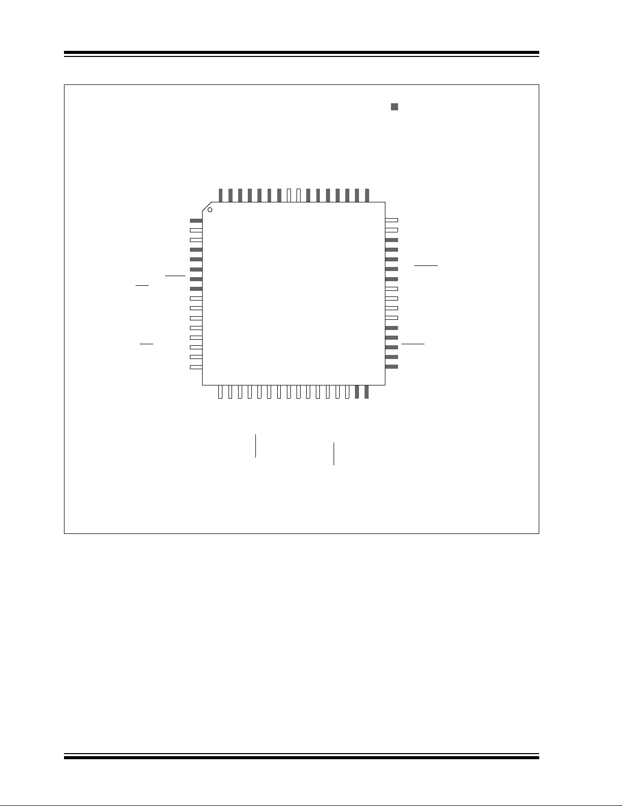
dsPIC33FJXXXGPX06/X08/X10
64-Pin TQFP
1
2
3
4
5
6
7
8
9
10
11
12
13
36
35
34
33
32
31
30
29
28
27
26
646362616059585756
14
15
16
171819202122232425
PGEC2/SOSCO/T1CK/CN0/RC14
PGED2/SOSCI/T4CK/CN1/RC13
OC1/RD0
IC4/INT4/RD11
IC2/U1CTS
/INT2/RD9
IC1/INT1/RD8
V
SS
OSC2/CLKO/RC15
OSC1/CLKIN/RC12
V
DD
SCL1/RG2
U1RTS
/SCK1/INT0/RF6
U1RX/SDI1/RF2
U1TX/SDO1/RF3
COFS/RG15
AN16/T2CK/T7CK/RC1
AN17/T3CK/T6CK/RC2
SCK2/CN8/RG6
SDI2/CN9/RG7
SDO2/CN10/RG8
MCLR
VSS
VDD
AN3/CN5/RB3
AN2/SS1
/CN4/RB2
PGEC3/AN1/V
REF-/CN3/RB1
PGED3/AN0/V
REF+/CN2/RB0
OC8/CN16/RD7
CSDO/RG13
CSDI/RG12
CSCK/RG14
V
CAP/VDDCORE
RG1
RF1
RG0
OC2/RD1
OC3/RD2
PGEC1/AN6/OCFA/RB6
PGED1/AN7/RB7
AVDD
AVSS
U2CTS/AN8/RB8
AN9/RB9
TMS/AN10/RB10
TDO/AN11/RB11
V
SS
VDD
TCK/AN12/RB12
TDI/AN13/RB13
U2RTS
/AN14/RB14
AN15/OCFB/CN12/RB15
U2TX/CN18/RF5
U2RX/CN17/RF4
SDA1/RG3
43
42
41
40
39
38
37
44
48
47
46
504951
545352
55
45
SS2
/CN11/RG9
AN5/IC8/CN7/RB5
AN4/IC7/CN6/RB4
IC3/INT3/RD10
VDD
RF0
OC4/RD3
OC7/CN15/RD6
OC6/IC6/CN14/RD5
OC5/IC5/CN13/RD4
dsPIC33FJ64GP206
dsPIC33FJ128GP206
= Pins are up to 5V tolerant
Pin Diagrams
DS70286C-page 4 © 2009 Microchip Technology Inc.
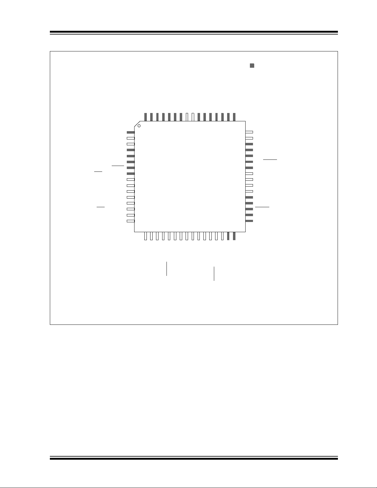
Pin Diagrams (Continued)
64-Pin TQFP
1
2
3
4
5
6
7
8
9
10
11
12
13
36
35
34
33
32
31
30
29
28
27
26
646362616059585756
14
15
16
171819202122232425
PGEC2/SOSCO/T1CK/CN0/RC14
PGED2/SOSCI/T4CK/CN1/RC13
OC1/RD0
IC4/INT4/RD11
IC2/U1CTS
/INT2/RD9
IC1/INT1/RD8
V
SS
OSC2/CLKO/RC15
OSC1/CLKIN/RC12
V
DD
SCL1/RG2
U1RTS
/SCK1/INT0/RF6
U1RX/SDI1/RF2
U1TX/SDO1/RF3
COFS/RG15
AN16/T2CK/T7CK/RC1
AN17/T3CK/T6CK/RC2
SCK2/CN8/RG6
SDI2/CN9/RG7
SDO2/CN10/RG8
MCLR
VSS
VDD
AN3/CN5/RB3
AN2/SS1
/CN4/RB2
PGEC3/AN1/V
REF-/CN3/RB1
PGED3/AN0/V
REF+/CN2/RB0
OC8/CN16/RD7
CSDO/RG13
CSDI/RG12
CSCK/RG14
V
CAP/VDDCORE
RG1
RF1
RG0
OC2/RD1
OC3/RD2
PGEC1/AN6/OCFA/RB6
PGED1/AN7/RB7
AVDD
AVSS
U2CTS/AN8/RB8
AN9/RB9
TMS/AN10/RB10
TDO/AN11/RB11
V
SS
VDD
TCK/AN12/RB12
TDI/AN13/RB13
U2RTS
/AN14/RB14
AN15/OCFB/CN12/RB15
U2TX/SCL2/CN18/RF5
U2RX/SDA2/CN17/RF4
SDA1/RG3
43
42
41
40
39
38
37
44
48
47
46
504951
545352
55
45
SS2
/CN11/RG9
AN5/IC8/CN7/RB5
AN4/IC7/CN6/RB4
IC3/INT3/RD10
VDD
RF0
OC4/RD3
OC7/CN15/RD6
OC6/IC6/CN14/RD5
OC5/IC5/CN13/RD4
dsPIC33FJ64GP306
dsPIC33FJ128GP306
= Pins are up to 5V tolerant
dsPIC33FJXXXGPX06/X08/X10
© 2009 Microchip Technology Inc. DS70286C-page 5

dsPIC33FJXXXGPX06/X08/X10
64-Pin TQFP
1
2
3
4
5
6
7
8
9
10
11
12
13
36
35
34
33
32
31
30
29
28
27
26
646362616059585756
14
15
16
171819202122232425
PGEC2/SOSCO/T1CK/CN0/RC14
PGED2/SOSCI/T4CK/CN1/RC13
OC1/RD0
IC4/INT4/RD11
IC2/U1CTS
/INT2/RD9
IC1/INT1/RD8
V
SS
OSC2/CLKO/RC15
OSC1/CLKIN/RC12
V
DD
SCL1/RG2
U1RTS
/SCK1/INT0/RF6
U1RX/SDI1/RF2
U1TX/SDO1/RF3
COFS/RG15
AN16/T2CK/T7CK/RC1
AN17/T3CK/T6CK/RC2
SCK2/CN8/RG6
SDI2/CN9/RG7
SDO2/CN10/RG8
MCLR
VSS
VDD
AN3/CN5/RB3
AN2/SS1
/CN4/RB2
PGEC3/AN1/V
REF-/CN3/RB1
PGED3/AN0/V
REF+/CN2/RB0
OC8/CN16/RD7
CSDO/RG13
CSDI/RG12
CSCK/RG14
V
CAP/VDDCORE
RG1
C1TX/RF1
RG0
OC2/RD1
OC3/RD2
PGEC1/AN6/OCFA/RB6
PGED1/AN7/RB7
AVDD
AVSS
U2CTS/AN8/RB8
AN9/RB9
TMS/AN10/RB10
TDO/AN11/RB11
V
SS
VDD
TCK/AN12/RB12
TDI/AN13/RB13
U2RTS
/AN14/RB14
AN15/OCFB/CN12/RB15
U2TX/SCL2/CN18/RF5
U2RX/SDA2/CN17/RF4
SDA1/RG3
43
42
41
40
39
38
37
44
48
47
46
504951
545352
55
45
SS2
/CN11/RG9
AN5/IC8/CN7/RB5
AN4/IC7/CN6/RB4
IC3/INT3/RD10
VDD
C1RX/RF0
OC4/RD3
OC7/CN15/RD6
OC6/IC6/CN14/RD5
OC5/IC5/CN13/RD4
dsPIC33FJ256GP506
= Pins are up to 5V tolerant
Pin Diagrams (Continued)
DS70286C-page 6 © 2009 Microchip Technology Inc.
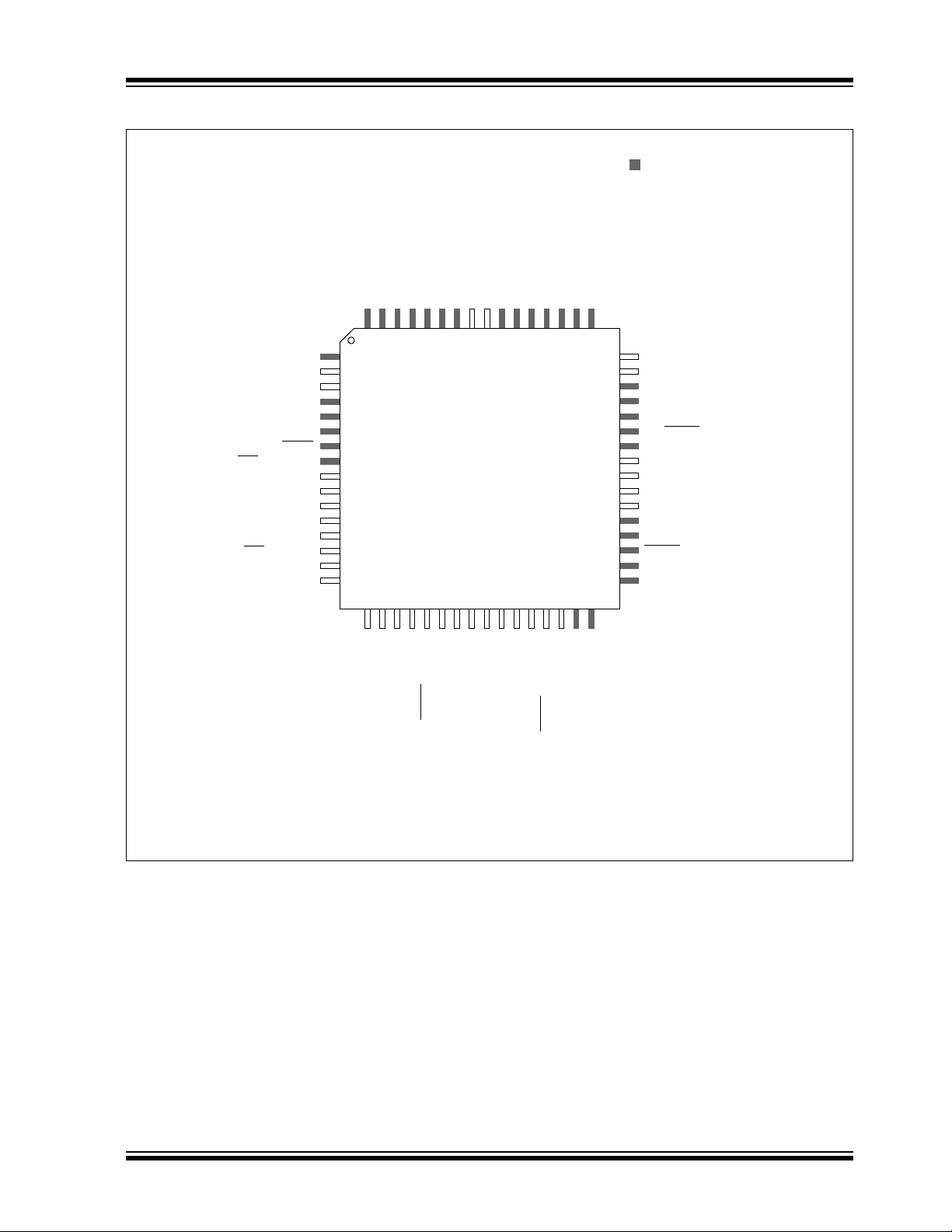
Pin Diagrams (Continued)
64-Pin TQFP
1
2
3
4
5
6
7
8
9
10
11
12
13
36
35
34
33
32
31
30
29
28
27
26
646362616059585756
14
15
16
171819202122232425
PGEC2/SOSCO/T1CK/CN0/RC14
PGED2/SOSCI/T4CK/CN1/RC13
OC1/RD0
IC4/INT4/RD11
IC2/U1CTS
/INT2/RD9
IC1/INT1/RD8
V
SS
OSC2/CLKO/RC15
OSC1/CLKIN/RC12
V
DD
SCL1/RG2
U1RTS
/SCK1/INT0/RF6
U1RX/SDI1/RF2
U1TX/SDO1/RF3
COFS/RG15
AN16/T2CK/T7CK/RC1
AN17/T3CK/T6CK/RC2
SCK2/CN8/RG6
SDI2/CN9/RG7
SDO2/CN10/RG8
MCLR
VSS
VDD
AN3/CN5/RB3
AN2/SS1
/CN4/RB2
PGEC3/AN1/V
REF-/CN3/RB1
PGED3/AN0/V
REF+/CN2/RB0
OC8/CN16/RD7
CSDO/RG13
CSDI/RG12
CSCK/RG14
V
CAP/VDDCORE
C2TX/RG1
C1TX/RF1
C2RX/RG0
OC2/RD1
OC3/RD2
PGEC1/AN6/OCFA/RB6
PGED1/AN7/RB7
AVDD
AVSS
U2CTS/AN8/RB8
AN9/RB9
TMS/AN10/RB10
TDO/AN11/RB11
V
SS
VDD
TCK/AN12/RB12
TDI/AN13/RB13
U2RTS
/AN14/RB14
AN15/OCFB/CN12/RB15
U2TX/SCL2/CN18/RF5
U2RX/SDA2/CN17/RF4
SDA1/RG3
43
42
41
40
39
38
37
44
48
47
46
504951
545352
55
45
SS2
/CN11/RG9
AN5/IC8/CN7/RB5
AN4/IC7/CN6/RB4
IC3/INT3/RD10
VDD
C1RX/RF0
OC4/RD3
OC7/CN15/RD6
OC6/IC6/CN14/RD5
OC5/IC5/CN13/RD4
dsPIC33FJ64GP706
dsPIC33FJ128GP706
= Pins are up to 5V tolerant
dsPIC33FJXXXGPX06/X08/X10
© 2009 Microchip Technology Inc. DS70286C-page 7
dsPIC33FJXXXGPX06/X08/X10
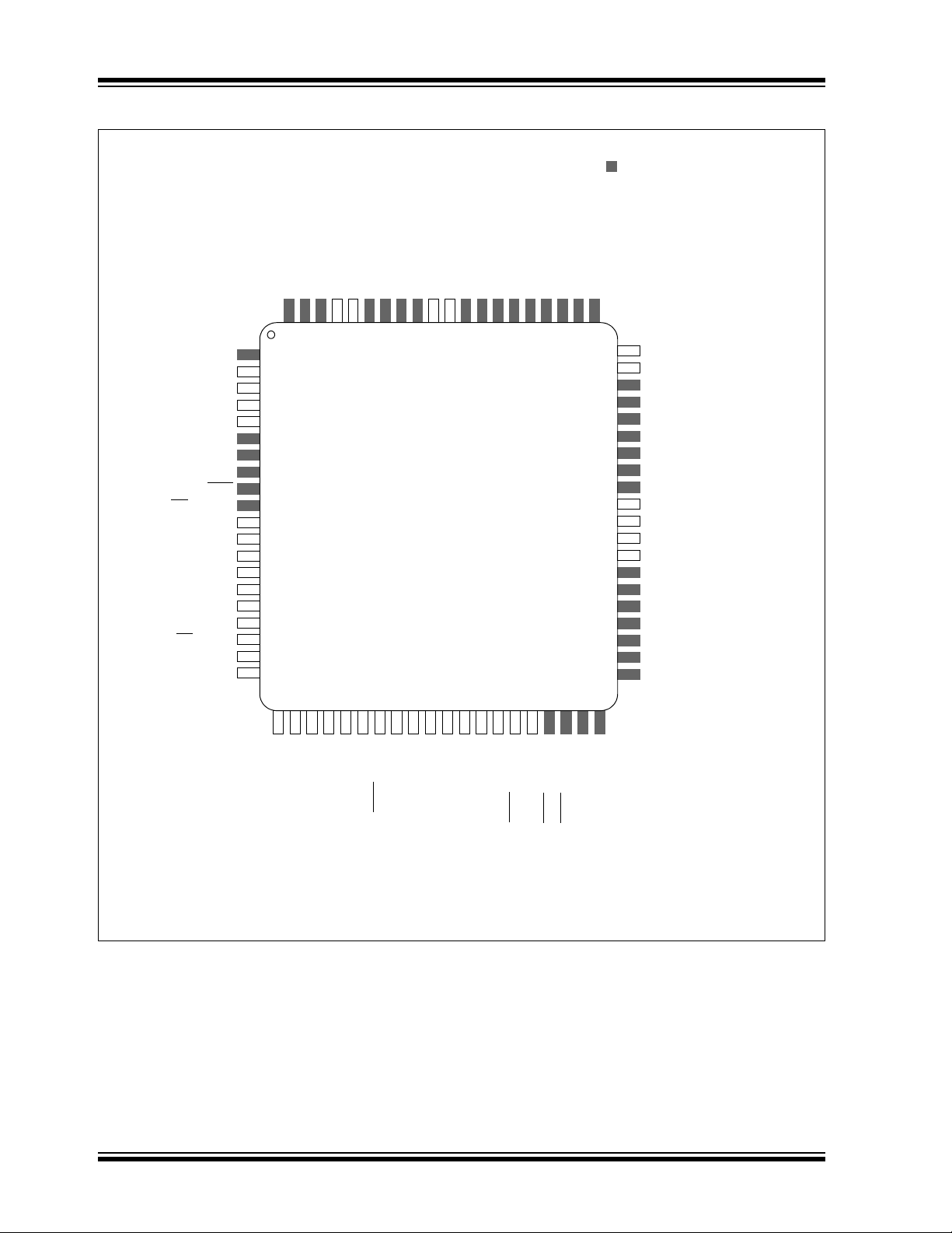
80-Pin TQFP
727473
7170696867666564636261
20
2
3
4
5
6
7
8
9
10
11
12
13
14
15
16
50
49
48
47
46
45
44
21
41
40
39
38
37
36
35
34
2324252627282930313233
dsPIC33FJ64GP708
17
18
19
75
1
57
56
55
54
53
52
51
60
59
58
43
42
767877
792280
IC5/RD12
OC4/RD3
OC3/RD2
OC2/RD1
CSCK/RG14
AN23/CN23/RA7
AN22/CN22/RA6
C2RX/RG0
C2TX/RG1
C1TX/RF1
C1RX/RF0
CSDO/RG13
CSDI/RG12
OC8/CN16/RD7
OC6/CN14/RD5
OC1/RD0
IC4/RD11
IC2/RD9
IC1/RD8
IC3/RD10
V
SS
OSC1/CLKIN/RC12
V
DD
SCL1/RG2
U1RX/RF2
U1TX/RF3
PGEC2/SOSCO/T1CK/CN0/RC14
PGED2/SOSCI/CN1/RC13
V
REF
+/RA10
V
REF
-/RA9
AV
DD
AV
SS
U2CTS/AN8/RB8
AN9/RB9
AN10/RB10
AN11/RB11
V
DD
U2RX/CN17/RF4
IC8/U1RTS
/CN21/RD15
U2TX/CN18/RF5
PGEC1/AN6/OCFA/RB6
PGED1/AN7/RB7
AN17/T3CK/T6CK/RC2
AN18/T4CK/T9CK/RC3
AN19/T5CK/T8CK/RC4
SCK2/CN8/RG6
SDI2/CN9/RG7
SDO2/CN10/RG8
MCLR
SS2/CN11/RG9
AN4/CN6/RB4
AN3/CN5/RB3
AN2/SS1
/CN4/RB2
PGEC3/AN1/CN3/RB1
PGED3/AN0/CN2/RB0
V
SS
V
DD
COFS/RG15
AN16/T2CK/T7CK/RC1
TDO/AN21/INT2/RA13
TMS/AN20/INT1/RA12
TCK/AN12/RB12
TDI/AN13/RB13
U2RTS
/AN14/RB14
AN15/OCFB/CN12/RB15
V
DDVCAP
/V
DDCORE
OC5/CN13/RD4
IC6/CN19/RD13
SDA1/RG3
SDI1/RF7
SDO1/RF8
AN5/CN7/RB5
V
SS
OSC2/CLKO/RC15
OC7/CN15/RD6
SCK1/INT0/RF6
IC7/U1CTS/CN20/RD14
SDA2/INT4/RA3
SCL2/INT3/RA2
dsPIC33FJ128GP708
= Pins are up to 5V tolerant
Pin Diagrams (Continued)
DS70286C-page 8 © 2009 Microchip Technology Inc.
Pin Diagrams (Continued)
9294939190898887868584838281807978
20
2
3
4
5
6
7
8
9
10
11
12
13
14
15
16
65
64
63
62
61
60
59
26
56
45
44
43
42
41
40
39
2829303132333435363738
17
18
19
21
22
95
1
76
77
72
71
70
69
68
67
66
75
74
73
58
57
24
23
25
969897
99
27
4647484950
55
54
53
52
51
OC6/CN14/RD5
OC5/CN13/RD4
IC6/CN19/RD13
IC5/RD12
OC4/RD3
OC3/RD2
OC2/RD1
AN23/CN23/RA7
AN22/CN22/RA6
AN26/RE2
CSDO/RG13
CSDI/RG12
CSCK/RG14
AN25/RE1
AN24/RE0
RG0
AN28/RE4
AN27/RE3
RF0
V
CAP
/V
DDCORE
PGED2/SOSCI/CN1/RC13
OC1/RD0
IC3/RD10
IC2/RD9
IC1/RD8
IC4/RD11
SDA2/RA3
SCL2/RA2
OSC2/CLKO/RC15
OSC1/CLKIN/RC12
V
DD
SCL1/RG2
SCK1/INT0/RF6
SDI1/RF7
SDO1/RF8
SDA1/RG3
U1RX/RF2
U1TX/RF3
V
SS
PGEC2/SOSCO/T1CK/CN0/RC14
V
REF
+/RA10
V
REF
-/RA9
AV
DD
AV
SS
AN8/RB8
AN9/RB9
AN10/RB10
AN11/RB11
V
DD
U2CTS/RF12
U2RTS
/RF13
IC7/U1CTS
/CN20/RD14
IC8/U1RTS
/CN21/RD15
V
DD
V
SS
PGEC1/AN6/OCFA/RB6
PGED1/AN7/RB7
U2TX/CN18/RF5
U2RX/CN17/RF4
AN29/RE5
AN30/RE6
AN31/RE7
AN16/T2CK/T7CK/RC1
AN17/T3CK/T6CK/RC2
AN18/T4CK/T9CK/RC3
AN19/T5CK/T8CK/RC4
SCK2/CN8/RG6
V
DD
TMS/RA0
AN20/INT1/RA12
AN21/INT2/RA13
AN5/CN7/RB5
AN4/CN6/RB4
AN3/CN5/RB3
AN2/SS1
/CN4/RB2
SDI2/CN9/RG7
SDO2/CN10/RG8
PGEC3/AN1/CN3/RB1
PGED3/AN0/CN2/RB0
COFS/RG15
V
DD
SS2/CN11/RG9
MCLR
AN12/RB12
AN13/RB13
AN14/RB14
AN15/OCFB/CN12/RB15
RG1
RF1
OC8/CN16/RD7
OC7/CN15/RD6
TDO/RA5
INT4/RA15
INT3/RA14
V
SS
V
SS
V
SS
V
DD
TDI/RA4
TCK/RA1
100-Pin TQFP
dsPIC33FJ64GP310
dsPIC33FJ128GP310
100
= Pins are up to 5V tolerant
dsPIC33FJXXXGPX06/X08/X10
© 2009 Microchip Technology Inc. DS70286C-page 9
dsPIC33FJXXXGPX06/X08/X10
9294939190898887868584838281807978
20
2
3
4
5
6
7
8
9
10
11
12
13
14
15
16
65
64
63
62
61
60
59
26
56
45
44
43
42
41
40
39
2829303132333435363738
17
18
19
21
22
95
1
76
77
72
71
70
69
68
67
66
75
74
73
58
57
24
23
25
969897
99
27
4647484950
55
54
53
52
51
OC6/CN14/RD5
OC5/CN13/RD4
IC6/CN19/RD13
IC5/RD12
OC4/RD3
OC3/RD2
OC2/RD1
AN23/CN23/RA7
AN22/CN22/RA6
AN26/RE2
CSDO/RG13
CSDI/RG12
CSCK/RG14
AN25/RE1
AN24/RE0
RG0
AN28/RE4
AN27/RE3
C1RX/RF0
V
CAP
/V
DDCORE
PGED2/SOSCI/CN1/RC13
OC1/RD0
IC3/RD10
IC2/RD9
IC1/RD8
IC4/RD11
SDA2/RA3
SCL2/RA2
OSC2/CLKO/RC15
OSC1/CLKIN/RC12
V
DD
SCL1/RG2
SCK1/INT0/RF6
SDI1/RF7
SDO1/RF8
SDA1/RG3
U1RX/RF2
U1TX/RF3
V
SS
PGEC2/SOSCO/T1CK/CN0/RC14
V
REF
+/RA10
V
REF
-/RA9
AV
DD
AV
SS
AN8/RB8
AN9/RB9
AN10/RB10
AN11/RB11
V
DD
U2CTS/RF12
U2RTS
/RF13
IC7/U1CTS
/CN20/RD14
IC8/U1RTS
/CN21/RD15
V
DD
V
SS
PGEC1/AN6/OCFA/RB6
PGED1/AN7/RB7
U2TX/CN18/RF5
U2RX/CN17/RF4
AN29/RE5
AN30/RE6
AN31/RE7
AN16/T2CK/T7CK/RC1
AN17/T3CK/T6CK/RC2
AN18/T4CK/T9CK/RC3
AN19/T5CK/T8CK/RC4
SCK2/CN8/RG6
V
DD
TMS/RA0
AN20/INT1/RA12
AN21/INT2/RA13
AN5/CN7/RB5
AN4/CN6/RB4
AN3/CN5/RB3
AN2/SS1
/CN4/RB2
SDI2/CN9/RG7
SDO2/CN10/RG8
PGEC3/AN1/CN3/RB1
PGED3/AN0/CN2/RB0
COFS/RG15
V
DD
SS2/CN11/RG9
MCLR
AN12/RB12
AN13/RB13
AN14/RB14
AN15/OCFB/CN12/RB15
RG1
C1TX/RF1
OC8/CN16/RD7
OC7/CN15/RD6
TDO/RA5
INT4/RA15
INT3/RA14
V
SS
V
SS
V
SS
V
DD
TDI/RA4
TCK/RA1
100-Pin TQFP
dsPIC33FJ256GP510
100
= Pins are up to 5V tolerant
Pin Diagrams (Continued)
DS70286C-page 10 © 2009 Microchip Technology Inc.
Pin Diagrams (Continued)
9294939190898887868584838281807978
20
2
3
4
5
6
7
8
9
10
11
12
13
14
15
16
65
64
63
62
61
60
59
26
56
45
44
43
42
41
40
39
2829303132333435363738
17
18
19
21
22
95
1
76
77
72
71
70
69
68
67
66
75
74
73
58
57
24
23
25
969897
99
27
4647484950
55
54
53
52
51
OC6/CN14/RD5
OC5/CN13/RD4
IC6/CN19/RD13
IC5/RD12
OC4/RD3
OC3/RD2
OC2/RD1
AN23/CN23/RA7
AN22/CN22/RA6
AN26/RE2
CSDO/RG13
CSDI/RG12
CSCK/RG14
AN25/RE1
AN24/RE0
C2RX/RG0
AN28/RE4
AN27/RE3
C1RX/RF0
V
CAP
/V
DDCORE
PGED2/SOSCI/CN1/RC13
OC1/RD0
IC3/RD10
IC2/RD9
IC1/RD8
IC4/RD11
SDA2/RA3
SCL2/RA2
OSC2/CLKO/RC15
OSC1/CLKIN/RC12
V
DD
SCL1/RG2
SCK1/INT0/RF6
SDI1/RF7
SDO1/RF8
SDA1/RG3
U1RX/RF2
U1TX/RF3
V
SS
PGEC2/SOSCO/T1CK/CN0/RC14
V
REF
+/RA10
V
REF
-/RA9
AV
DD
AV
SS
AN8/RB8
AN9/RB9
AN10/RB10
AN11/RB11
V
DD
U2CTS/RF12
U2RTS
/RF13
IC7/U1CTS
/CN20/RD14
IC8/U1RTS
/CN21/RD15
V
DD
V
SS
PGEC1/AN6/OCFA/RB6
PGED1/AN7/RB7
U2TX/CN18/RF5
U2RX/CN17/RF4
AN29/RE5
AN30/RE6
AN31/RE7
AN16/T2CK/T7CK/RC1
AN17/T3CK/T6CK/RC2
AN18/T4CK/T9CK/RC3
AN19/T5CK/T8CK/RC4
SCK2/CN8/RG6
V
DD
TMS/RA0
AN20/INT1/RA12
AN21/INT2/RA13
AN5/CN7/RB5
AN4/CN6/RB4
AN3/CN5/RB3
AN2/SS1
/CN4/RB2
SDI2/CN9/RG7
SDO2/CN10/RG8
PGEC3/AN1/CN3/RB1
PGED3/AN0/CN2/RB0
COFS/RG15
V
DD
SS2/CN11/RG9
MCLR
AN12/RB12
AN13/RB13
AN14/RB14
AN15/OCFB/CN12/RB15
C2TX/RG1
C1TX/RF1
OC8/CN16/RD7
OC7/CN15/RD6
TDO/RA5
INT4/RA15
INT3/RA14
V
SS
V
SS
V
SS
V
DD
TDI/RA4
TCK/RA1
100-Pin TQFP
dsPIC33FJ128GP710
100
dsPIC33FJ256GP710
dsPIC33FJ64GP710
= Pins are up to 5V tolerant
dsPIC33FJXXXGPX06/X08/X10
© 2009 Microchip Technology Inc. DS70286C-page 11

dsPIC33FJXXXGPX06/X08/X10
Table of Contents
dsPIC33F Product Families ................................................................................................................................................................... 3
1.0 Device Overview ........................................................................................................................................................................ 13
2.0 Guidelines for Getting Started with 16-Bit Digital Signal Controllers .......................................................................................... 17
3.0 CPU............................................................................................................................................................................................ 21
4.0 Memory Organization ................................................................................................................................................................. 33
5.0 Flash Program Memory.............................................................................................................................................................. 71
6.0 Reset ......................................................................................................................................................................................... 77
7.0 Interrupt Controller ..................................................................................................................................................................... 81
8.0 Direct Memory Access (DMA) .................................................................................................................................................. 127
9.0 Oscillator Configuration ............................................................................................................................................................ 137
10.0 Power-Saving Features ............................................................................................................................................................ 147
11.0 I/O Ports ................................................................................................................................................................................... 155
12.0 Timer1 ...................................................................................................................................................................................... 157
13.0 Timer2/3, Timer4/5, Timer6/7 and Timer8/9 ............................................................................................................................ 159
14.0 Input Capture............................................................................................................................................................................ 165
15.0 Output Compare ....................................................................................................................................................................... 167
16.0 Serial Peripheral Interface (SPI)............................................................................................................................................... 171
17.0 Inter-Integrated Circuit™ (I
18.0 Universal Asynchronous Receiver Transmitter (UART) ........................................................................................................... 185
19.0 Enhanced CAN (ECAN™) Module ........................................................................................................................................... 191
20.0 Data Converter Interface (DCI) Module.................................................................................................................................... 217
21.0 10-Bit/12-Bit Analog-to-Digital Converter (ADC) ...................................................................................................................... 225
22.0 Special Features ...................................................................................................................................................................... 237
23.0 Instruction Set Summary .......................................................................................................................................................... 245
24.0 Development Support............................................................................................................................................................... 253
25.0 Electrical Characteristics .......................................................................................................................................................... 257
26.0 Packaging Information.............................................................................................................................................................. 297
Appendix A: Revision History............................................................................................................................................................. 307
Index ................................................................................................................................................................................................. 313
The Microchip Web Site ..................................................................................................................................................................... 317
Customer Change Notification Service .............................................................................................................................................. 317
Customer Support .............................................................................................................................................................................. 317
Reader Response .............................................................................................................................................................................. 318
Product Identification System............................................................................................................................................................. 319
2
C™).............................................................................................................................................. 177
TO OUR VALUED CUSTOMERS
It is our intention to provide our valued customers with the best documentation possible to ensure successful use of your Microchip
products. To this end, we will continue to improve our publications to better suit your needs. Our publications will be refined and
enhanced as new volumes and updates are introduced.
If you have any questions or comments regarding this publication, please contact the Marketing Communications Department via
E-mail at docerrors@microchip.com or fax the Reader Response Form in the back of this data sheet to (480) 792-4150. We
welcome your feedback.
Most Current Data Sheet
To obtain the most up-to-date version of this data sheet, please register at our Worldwide Web site at:
http://www.microchip.com
You can determine the version of a data sheet by examining its literature number found on the bottom outside corner of any page.
The last character of the literature number is the version number, (e.g., DS30000A is version A of document DS30000).
Errata
An errata sheet, describing minor operational differences from the data sheet and recommended workarounds, may exist for current
devices. As device/documentation issues become known to us, we will publish an errata sheet. The errata will specify the revision
of silicon and revision of document to which it applies.
To determine if an errata sheet exists for a particular device, please check with one of the following:
• Microchip’s Worldwide Web site; http://www.microchip.com
• Your local Microchip sales office (see last page)
When contacting a sales office, please specify which device, revision of silicon and data sheet (include literature number) you are
using.
Customer Notification System
Register on our web site at www.microchip.com to receive the most current information on all of our products.
DS70286C-page 12 © 2009 Microchip Technology Inc.

dsPIC33FJXXXGPX06/X08/X10
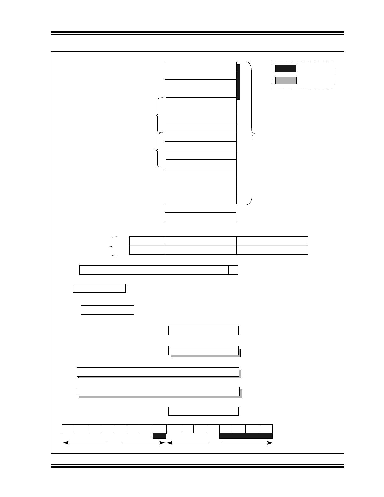
1.0 DEVICE OVERVIEW
Note: This data sheet summarizes the features
of the dsPIC33FJXXXGPX06/X08/X10
family of devices. However, it is not
intended to be a comprehensive reference
source. To complement the information in
this data sheet, refer to the latest family
reference sections of the “dsPIC33F
Family Reference Manual”, which is
available from the Microchip web site
(www.microchip.com).
This document contains device specific information for
the following devices:
• dsPIC33FJ64GP206
• dsPIC33FJ64GP306
• dsPIC33FJ64GP310
• dsPIC33FJ64GP706
• dsPIC33FJ64GP708
• dsPIC33FJ64GP710
• dsPIC33FJ128GP206
• dsPIC33FJ128GP306
• dsPIC33FJ128GP310
• dsPIC33FJ128GP706
• dsPIC33FJ128GP708
• dsPIC33FJ128GP710
• dsPIC33FJ256GP506
• dsPIC33FJ256GP510
• dsPIC33FJ256GP710
The dsPIC33FJXXXGPX06/X08/X10 General Purpose
Family of device includes devices with a wide range of
pin counts (64, 80 and 100), different program memory
sizes (64 Kbytes, 128 Kbytes and 256 Kbytes) and
different RAM sizes (8 Kbytes, 16 Kbytes and
30 Kbytes).
This feature makes the family suitable for a wide variety
of high-performance digital signal control applications.
The device is pin compatible with the PIC24H family of
devices, and also share a very high degree of
compatibility with the dsPIC30F family devices. This
allows for easy migration between device families as may
be necessitated by the specific functionality,
computational resource and system cost requirements of
the application.
The dsPIC33FJXXXGPX06/X08/X10 device family
employs a powerful 16-bit architecture that seamlessly
integrates the control features of a Microcontroller
(MCU) with the computational capabilities of a Digital
Signal Processor (DSP). The resulting functionality is
ideal for applications that rely on high-speed, repetitive
computations, as well as control.
The DSP engine, dual 40-bit accumulators, hardware
support for division operations, barrel shifter, 17 x 17
multiplier, a large array of 16-bit working registers and
a wide variety of data addressing modes, together
provide the dsPIC33FJXXXGPX06/X08/X10 Central
Processing Unit (CPU) with extensive mathematical
processing capability. Flexible and deterministic
interrupt handling, coupled with a powerful array of
peripherals, renders the
dsPIC33FJXXXGPX06/X08/X10 devices suitable for
control applications. Further, Direct Memory Access
(DMA) enables overhead-free transfer of data between
several peripherals and a dedicated DMA RAM.
Reliable, field programmable Flash program memory
ensures scalability of applications that use
dsPIC33FJXXXGPX06/X08/X10 devices.
Figure 1-1 illustrates a general block diagram of the
various core and peripheral modules in the
dsPIC33FJXXXGPX06/X08/X10 family of devices.
Table 1-1 provides the functions of the various pins
illustrated in the pinout diagrams.
© 2009 Microchip Technology Inc. DS70286C-page 13
16
OSC1/CLKI
OSC2/CLKO
V
DD, VSS
Timing
Generation
MCLR
Power-up
Timer
Oscillator
Star t- up Timer
Power-on
Reset
Watchdog
Timer
Brown-out
Reset
Precision
Reference
Band Gap
FRC/LPRC
Oscillators
Regulator
Voltage
VCAP/VDDCORE
UART1,2
ECAN1,2
DCI
IC1-8
SPI1,2
I2C1,2
OC/
PORTA
Note: Not all pins or features are implemented on all device pinout configurations. See pinout diagrams for the specific pins
and features present on each device.
PWM1-8
CN1-23
Instruction
Decode and
Control
PCH PCL
16
Program Counter
16-bit ALU
23
23
24
23
Instruction Reg
PCU
16 x 16
W Register Array
ROM Latch
16
EA MUX
16
16
8
Interrupt
Controller
PSV and Table
Data Access
Control Block
Stac k
Control
Logic
Loop
Control
Logic
Data Latch
Address
Latch
Address Latch
Program Memory
Data Latch
Literal Data
16
16
16
16
Data Latch
Address
Latch
16
X RAM
Y RAM
16
Y Data Bus
X Data Bus
DSP Engine
Divide Support
16
DMA
RAM
DMA
Controller
Control Signals
to Various Blocks
ADC1,2
Timers
PORTB
PORTC
PORTD
PORTE
PORTF
PORTG
Address Generator Units
1-9
dsPIC33FJXXXGPX06/X08/X10
FIGURE 1-1: dsPIC33FJXXXGPX06/X08/X10 GENERAL BLOCK DIAGRAM
DS70286C-page 14 © 2009 Microchip Technology Inc.

dsPIC33FJXXXGPX06/X08/X10
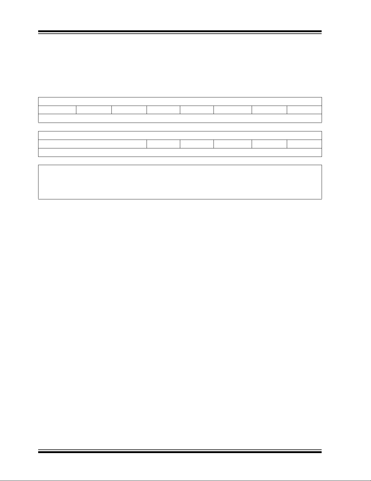
TABLE 1-1: PINOUT I/O DESCRIPTIONS
Pin Name
AN0-AN31 I Analog Analog input channels.
DD P P Positive supply for analog modules. This pin must be connected at all times.
AV
AV
SS P P Ground reference for analog modules.
CLKI
CLKO
CN0-CN23 I ST Input change notification inputs.
COFS
CSCK
CSDI
CSDO
C1RX
C1TX
C2RX
C2TX
PGED1
PGEC1
PGED2
PGEC2
PGED3
PGEC3
IC1-IC8 I ST Capture inputs 1 through 8.
INT0
INT1
INT2
INT3
INT4
MCLR
OCFA
OCFB
OC1-OC8
OSC1
OSC2
RA0-RA7
RA9-RA10
RA12-RA15
RB0-RB15 I/O ST PORTB is a bidirectional I/O port.
RC1-RC4
RC12-RC15
RD0-RD15 I/O ST PORTD is a bidirectional I/O port.
RE0-RE7 I/O ST PORTE is a bidirectional I/O port.
RF0-RF8
RF12-RF13
Legend: CMOS = CMOS compatible input or output; Analog = Analog input; P = Power
ST = Schmitt Trigger input with CMOS levels; O = Output; I = Input
Pin
Type
I
O
I/O
I/O
I
O
I
O
I
O
I/O
I
I/O
I
I/O
I
I
I
I
I
I
I/P ST Master Clear (Reset) input. This pin is an active-low Reset to the device.
I
I
O
I
I/O
I/O
I/O
I/O
I/O
I/O
I/O
I/O
Buffer
Typ e
ST/CMOS—External clock source input. Always associated with OSC1 pin function.
Oscillator crystal output. Connects to crystal or resonator in Crystal Oscillator
mode. Optionally functions as CLKO in RC and EC modes. Always associated
with OSC2 pin function.
Can be software programmed for internal weak pull-ups on all inputs.
ST
ST
ST
—
ST
—
ST
—
ST
ST
ST
ST
ST
ST
ST
ST
ST
ST
ST
ST
ST
—
ST/CMOS—Oscillator crystal input. ST buffer when configured in RC mode;
ST
ST
ST
ST
ST
ST
ST
Data Converter Interface frame synchronization pin.
Data Converter Interface serial clock input/output pin.
Data Converter Interface serial data input pin.
Data Converter Interface serial data output pin.
ECAN1 bus receive pin.
ECAN1 bus transmit pin.
ECAN2 bus receive pin.
ECAN2 bus transmit pin.
Data I/O pin for programming/debugging communication channel 1.
Clock input pin for programming/debugging communication channel 1.
Data I/O pin for programming/debugging communication channel 2.
Clock input pin for programming/debugging communication channel 2.
Data I/O pin for programming/debugging communication channel 3.
Clock input pin for programming/debugging communication channel 3.
External interrupt 0.
External interrupt 1.
External interrupt 2.
External interrupt 3.
External interrupt 4.
Compare Fault A input (for Compare Channels 1, 2, 3 and 4).
Compare Fault B input (for Compare Channels 5, 6, 7 and 8).
Compare outputs 1 through 8.
CMOS otherwise.
Oscillator crystal output. Connects to crystal or resonator in Crystal Oscillator
mode. Optionally functions as CLKO in RC and EC modes.
PORTA is a bidirectional I/O port.
PORTC is a bidirectional I/O port.
PORTF is a bidirectional I/O port.
Description
© 2009 Microchip Technology Inc. DS70286C-page 15
dsPIC33FJXXXGPX06/X08/X10
TABLE 1-1: PINOUT I/O DESCRIPTIONS (CONTINUED)
Pin Name
RG0-RG3
RG6-RG9
RG12-RG15
SCK1
SDI1
SDO1
SS1
SCK2
SDI2
SDO2
SS2
SCL1
SDA1
SCL2
SDA2
SOSCI
SOSCO
TMS
TCK
TDI
TDO
T1CK
T2CK
T3CK
T4CK
T5CK
T6CK
T7CK
T8CK
T9CK
U1CTS
U1RTS
U1RX
U1TX
U2CTS
U2RTS
U2RX
U2TX
DD P — Positive supply for peripheral logic and I/O pins.
V
V
CAP/VDDCORE P — CPU logic filter capacitor connection.
VSS P — Ground reference for logic and I/O pins.
V
REF+ I Analog Analog voltage reference (high) input.
V
REF- I Analog Analog voltage reference (low) input.
Legend: CMOS = CMOS compatible input or output; Analog = Analog input; P = Power
ST = Schmitt Trigger input with CMOS levels; O = Output; I = Input
Pin
Type
I/O
I/O
I/O
I/O
I
O
I/O
I/O
I
O
I/O
I/O
I/O
I/O
I/O
I
O
I
I
I
O
I
I
I
I
I
I
I
I
I
I
O
I
O
I
O
I
O
Buffer
Typ e
ST
ST
ST
ST
ST
—
ST
ST
ST
—
ST
ST
ST
ST
ST
ST/CMOS—32.768 kHz low-power oscillator crystal input; CMOS otherwise.
ST
ST
ST
—
ST
ST
ST
ST
ST
ST
ST
ST
ST
ST
—
ST
—
ST
—
ST
—
PORTG is a bidirectional I/O port.
Synchronous serial clock input/output for SPI1.
SPI1 data in.
SPI1 data out.
SPI1 slave synchronization or frame pulse I/O.
Synchronous serial clock input/output for SPI2.
SPI2 data in.
SPI2 data out.
SPI2 slave synchronization or frame pulse I/O.
Synchronous serial clock input/output for I2C1.
Synchronous serial data input/output for I2C1.
Synchronous serial clock input/output for I2C2.
Synchronous serial data input/output for I2C2.
32.768 kHz low-power oscillator crystal output.
JTAG Test mode select pin.
JTAG test clock input pin.
JTAG test data input pin.
JTAG test data output pin.
Timer1 external clock input.
Timer2 external clock input.
Timer3 external clock input.
Timer4 external clock input.
Timer5 external clock input.
Timer6 external clock input.
Timer7 external clock input.
Timer8 external clock input.
Timer9 external clock input.
UART1 clear to send.
UART1 ready to send.
UART1 receive.
UART1 transmit.
UART2 clear to send.
UART2 ready to send.
UART2 receive.
UART2 transmit.
Description
DS70286C-page 16 © 2009 Microchip Technology Inc.

dsPIC33FJXXXGPX06/X08/X10
2.0 GUIDELINES FOR GETTING STARTED WITH 16-BIT DIGITAL SIGNAL CONTROLLERS
Note: This data sheet summarizes the features
of the dsPIC33FJXXXGPX06/X08/X10
family of devices. It is not intended to be a
comprehensive reference source. To
complement the information in this data
sheet, refer to the “dsPIC33F Family
Reference Manual”, which is available
from the Microchip website
(www.microchip.com).
2.1 Basic Connection Requirements
Getting started with the
dsPIC33FJXXXGPX06/X08/X10 family of 16-bit Digital
Signal Controllers (DSCs) requires attention to a
minimal set of device pin connections before
proceeding with development. The following is a list of
pin names, which must always be connected:
DD and VSS pins
• All V
(see Section 2.2 “Decoupling Capacitors”)
• All AV
•V
•MCLR
• PGECx/PGEDx pins used for In-Circuit Serial
• OSC1 and OSC2 pins when external oscillator
Additionally, the following pins may be required:
•V
DD and AVSS pins (regardless if ADC module
is not used)
(see Section 2.2 “Decoupling Capacitors”)
CAP/VDDCORE
(see Section 2.3 “Capacitor on Internal Voltage
Regulator (V
(see Section 2.4 “Master Clear (MCLR) Pin”)
Programming™ (ICSP™) and debugging purposes
(see Section 2.5 “ICSP Pins”)
source is used
(see Section 2.6 “External Oscillator Pins”)
REF+/VREF- pins used when external voltage
reference for ADC module is implemented
Note: The AVDD and AVSS pins must be
CAP/VDDCORE)”)
pin
connected independent of the ADC
voltage reference source.
2.2 Decoupling Capacitors
The use of decoupling capacitors on every pair of
power supply pins, such as V
AVSS is required.
Consider the following criteria when using decoupling
capacitors:
• Value and type of capacitor: Recommendation
of 0.1 µF (100 nF), 10-20V. This capacitor should
be a low-ESR and have resonance frequency in
the range of 20 MHz and higher. It is
recommended that ceramic capacitors be used.
• Placement on the printed circuit board: The
decoupling capacitors should be placed as close
to the pins as possible. It is recommended to
place the capacitors on the same side of the
board as the device. If space is constricted, the
capacitor can be placed on another layer on the
PCB using a via; however, ensure that the trace
length from the pin to the capacitor is within
one-quarter inch (6 mm) in length.
• Handling high frequency noise: If the board is
experiencing high frequency noise, upward of
tens of MHz, add a second ceramic-type capacitor
in parallel to the above described decoupling
capacitor. The value of the second capacitor can
be in the range of 0.01 µF to 0.001 µF. Place this
second capacitor next to the primary decoupling
capacitor. In high-speed circuit designs, consider
implementing a decade pair of capacitances as
close to the power and ground pins as possible.
For example, 0.1 µF in parallel with 0.001 µF.
• Maximizing performance: On the board layout
from the power supply circuit, run the power and
return traces to the decoupling capacitors first,
and then to the device pins. This ensures that the
decoupling capacitors are first in the power chain.
Equally important is to keep the trace length
between the capacitor and the power pins to a
minimum thereby reducing PCB track inductance.
DD, VSS, AVDD and
© 2009 Microchip Technology Inc. DS70286C-page 17
dsPIC33FJXXXGPX06/X08/X10
dsPIC33F
VDD
VSS
VDD
VSS
VSS
VDD
AVDD
AVSS
VDD
VSS
0.1 µF
Ceramic
0.1 µF
Ceramic
0.1 µF
Ceramic
0.1 µF
Ceramic
C
R
V
DD
MCLR
0.1 µF
Ceramic
VCAP/VDDCORE
10 Ω
R1
Note 1: R ≤ 10 kΩ is recommended. A suggested
starting value is 10 kΩ. Ensure that the
MCLR
pin VIH and VIL specifications are met.
2: R1 ≤ 470Ω will limit any current flowing into
MCLR
from the external capacitor C, in the
event of MCLR
pin breakdown, due to
Electrostatic Discharge (ESD) or Electrical
Overstress (EOS). Ensure that the MCLR
pin
V
IH and VIL specifications are met.
C
R1
R
V
DD
MCLR
dsPIC33F
JP
FIGURE 2-1: RECOMMENDED
MINIMUM CONNECTION
2.2.1 TANK CAPACITORS
On boards with power traces running longer than six
inches in length, it is suggested to use a tank capacitor
for integrated circuits including DSCs to supply a local
power source. The value of the tank capacitor should
be determined based on the trace resistance that connects the power supply source to the device, and the
maximum current drawn by the device in the application. In other words, select the tank capacitor so that it
meets the acceptable voltage sag at the device. Typical
values range from 4.7 µF to 47 µF.
2.4 Master Clear (MCLR) Pin
The MCLR pin provides for two specific device
functions:
• Device Reset
• Device programming and debugging
During device programming and debugging, the
resistance and capacitance that can be added to the
pin must be considered. Device programmers and
debuggers drive the MCLR
specific voltage levels (VIH and VIL) and fast signal
transitions must not be adversely affected. Therefore,
specific values of R and C will need to be adjusted
based on the application and PCB requirements.
For example, as shown in Figure 2-2, it is
recommended that the capacitor C, be isolated from
the MCLR
pin during programming and debugging
operations.
Place the components shown in Figure 2-2 within
one-quarter inch (6 mm) from the MCLR
FIGURE 2-2: EXAMPLE OF MCLR PIN
CONNECTIONS
pin. Consequently,
pin.
2.3 Capacitor on Internal Voltage
Regulator (V
A low-ESR (< 5 Ohms) capacitor is required on the
CAP/VDDCORE pin, which is used to stabilize the
V
voltage regulator output voltage. The V
pin must not be connected to VDD, and must have a
capacitor between 4.7 µF and 10 µF, 16V connected to
ground. The type can be ceramic or tantalum. Refer to
Section 25.0 “Electrical Characteristics” for
additional information.
The placement of this capacitor should be close to the
CAP/VDDCORE. It is recommended that the trace
V
length not exceed one-quarter inch (6 mm). Refer to
Section 22.2 “On-Chip Voltage Regulator” for
details.
DS70286C-page 18 © 2009 Microchip Technology Inc.
CAP/VDDCORE)
CAP/VDDCORE
dsPIC33FJXXXGPX06/X08/X10
13
Main Oscillator
Guard Ring
Guard Trace
Secondary
Oscillator
14
15
16
17
18
19
20
2.5 ICSP Pins
The PGECx and PGEDx pins are used for In-Circuit
Serial Programming™ (ICSP™) and debugging purposes. It is recommended to keep the trace length
between the ICSP connector and the ICSP pins on the
device as short as possible. If the ICSP connector is
expected to experience an ESD event, a series resistor
is recommended, with the value in the range of a few
tens of Ohms, not to exceed 100 Ohms.
Pull-up resistors, series diodes, and capacitors on the
PGECx and PGEDx pins are not recommended as they
will interfere with the programmer/debugger communications to the device. If such discrete components are
an application requirement, they should be removed
from the circuit during programming and debugging.
Alternatively, refer to the AC/DC characteristics and
timing requirements information in the respective
device Flash programming specification for information
on capacitive loading limits and pin input voltage high
IH) and input low (VIL) requirements.
(V
Ensure that the “Communication Channel Select” (i.e.,
PGECx/PGEDx pins) programmed into the device
matches the physical connections for the ICSP to
®
MPLAB
ICE™.
For more information on ICD 2, ICD 3 and REAL ICE
connection requirements, refer to the following
documents that are available on the Microchip website.
• “MPLAB
• “Using MPLAB
• “MPLAB
• “Using MPLAB
• “MPLAB
• “MPLAB
• “Using MPLAB
ICD 2, MPLAB ICD 3, or MPLAB REAL
®
ICD 2 In-Circuit Debugger User’s
Guide” DS51331
®
®
ICD 2” (poster) DS51265
ICD 2 Design Advisory” DS51566
®
ICD 3 In-Circuit Debugger”
(poster) DS51765
®
ICD 3 Design Advisory” DS51764
®
REAL ICE™ In-Circuit Emulator User’s
Guide” DS51616
®
REAL ICE™” (poster) DS51749
2.6 External Oscillator Pins
Many DSCs have options for at least two oscillators: a
high-frequency primary oscillator and a low-frequency
secondary oscillator (refer to Section 9.0 “Oscillator
Configuration” for details).
The oscillator circuit should be placed on the same
side of the board as the device. Also, place the
oscillator circuit close to the respective oscillator pins,
not exceeding one-half inch (12 mm) distance
between them. The load capacitors should be placed
next to the oscillator itself, on the same side of the
board. Use a grounded copper pour around the
oscillator circuit to isolate them from surrounding
circuits. The grounded copper pour should be routed
directly to the MCU ground. Do not run any signal
traces or power traces inside the ground pour. Also, if
using a two-sided board, avoid any traces on the
other side of the board where the crystal is placed. A
suggested layout is shown in Figure 2-3.
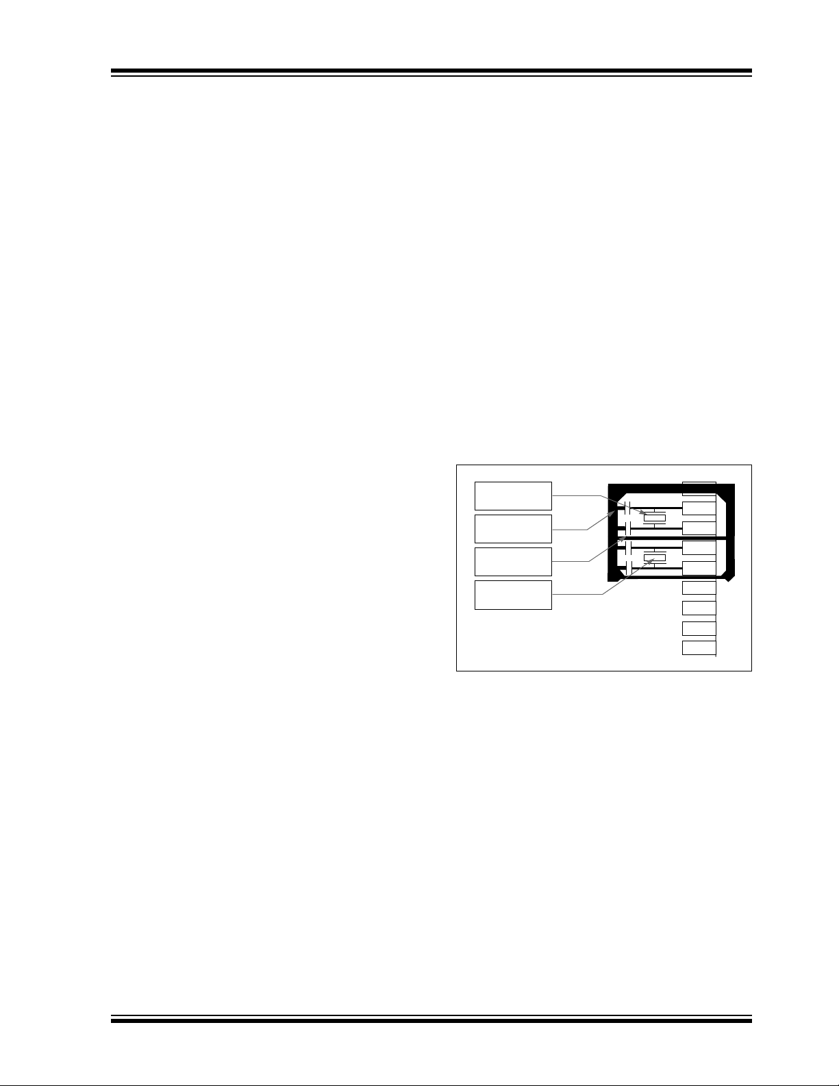
FIGURE 2-3: SUGGESTED PLACEMENT
OF THE OSCILLATOR
CIRCUIT
© 2009 Microchip Technology Inc. DS70286C-page 19

dsPIC33FJXXXGPX06/X08/X10
2.7 Oscillator Value Conditions on Device Start-up
If the PLL of the target device is enabled and
configured for the device start-up oscillator, the
maximum oscillator source frequency must be limited
to 4 MHz < F
start-up conditions. This means that if the external
oscillator frequency is outside this range, the
application must start-up in the FRC mode first. The
default PLL settings after a POR with an oscillator
frequency outside this range will violate the device
operating speed.
Once the device powers up, the application firmware
can initialize the PLL SFRs, CLKDIV and PLLDBF to a
suitable value, and then perform a clock switch to the
Oscillator + PLL clock source. Note that clock switching
must be enabled in the device Configuration word.
2.8 Configuration of Analog and
IN < 8 MHz to comply with device PLL
Digital Pins During ICSP
Operations
If MPLAB ICD 2, ICD 3 or REAL ICE is selected as a
debugger, it automatically initializes all of the A/D input
pins (ANx) as “digital” pins, by setting all bits in the
ADPCFG and ADPCFG2 registers.
The bits in the registers that correspond to the A/D pins
that are initialized by MPLAB ICD 2, ICD 3, or REAL
ICE, must not be cleared by the user application
firmware; otherwise, communication errors will result
between the debugger and the device.
If your application needs to use certain A/D pins as
analog input pins during the debug session, the user
application must clear the corresponding bits in the
ADPCFG and ADPCFG2 registers during initialization
of the ADC module.
When MPLAB ICD 2, ICD 3 or REAL ICE is used as a
programmer, the user application firmware must
correctly configure the ADPCFG and ADPCFG2
registers. Automatic initialization of these registers is
only done during debugger operation. Failure to
correctly configure the register(s) will result in all A/D
pins being recognized as analog input pins, resulting in
the port value being read as a logic ‘0’, which may
affect user application functionality.
2.9 Unused I/Os
Unused I/O pins should be configured as outputs and
driven to a logic-low state.
Alternatively, connect a 1k to 10k resistor to V
unused pins and drive the output to logic low.
DS70286C-page 20 © 2009 Microchip Technology Inc.
SS on

dsPIC33FJXXXGPX06/X08/X10
3.0 CPU
Note: This data sheet summarizes the features
of the dsPIC33FJXXXGPX06/X08/X10
family of devices. However, it is not
intended to be a comprehensive reference
source. To complement the information in
this data sheet, refer to Section 2. “CPU”
(DS70204) in the “dsPIC33F Family Ref-
erence Manual”, which is available from
the Microchip web site
(www.microchip.com).
The dsPIC33FJXXXGPX06/X08/X10 CPU module has a
16-bit (data) modified Harvard architecture with an
enhanced instruction set, including significant support for
DSP. The CPU has a 24-bit instruction word with a variable
length opcode field. The Program Counter (PC) is 23 bits
wide and addresses up to 4M x 24 bits of user program
memory space. The actual amount of program memory
implemented varies by device. A single-cycle instruction
prefetch mechanism is used to help maintain throughput
and provides predictable execution. All instructions execute
in a single cycle, with the exception of instructions that
MOV.D
DO
)
and
change the program flow, the double word move (
instruction and the table instructions. Overhead-free program loop constructs are supported using the
REPEAT
point.
The dsPIC33FJXXXGPX06/X08/X10 devices have sixteen,
16-bit working registers in the programmer’s model. Each of
the working registers can serve as a data, address or
address offset register. The 16th working register (W15)
operates as a software Stack Pointer (SP) for interrupts and
calls.
The dsPIC33FJXXXGPX06/X08/X10 instruction set has
two classes of instructions: MCU and DSP. These two
instruction classes are seamlessly integrated into a single
CPU. The instruction set includes many addressing modes
and is designed for optimum C compiler efficiency. For most
instructions, the dsPIC33FJXXXGPX06/X08/X10 is capable of executing a data (or program data) memory read, a
working register (data) read, a data memory write and a
program (instruction) memory read per instruction cycle. As
a result, three parameter instructions can be supported,
allowing A + B = C operations to be executed in a single
cycle.
A block diagram of the CPU is shown in Figure 3-1. The
programmer’s model for the
dsPIC33FJXXXGPX06/X08/X10 is shown in Figure 3-2.
instructions, both of which are interruptible at any
3.1 Data Addressing Overview
The data space can be addressed as 32K words or
64 Kbytes and is split into two blocks, referred to as X and
Y data memory. Each memory block has its own independent Address Generation Unit (AGU). The MCU class of
instructions operates solely through the X memory AGU,
which accesses the entire memory map as one linear data
space. Certain DSP instructions operate through the X and
Y AGUs to support dual operand reads, which splits the
data address space into two parts. The X and Y data space
boundary is device-specific.
Overhead-free circular buffers (Modulo Addressing mode)
are supported in both X and Y address spaces. The Modulo
Addressing removes the software boundary checking overhead for DSP algorithms. Furthermore, the X AGU circular
addressing can be used with any of the MCU class of
instructions. The X AGU also supports Bit-Reversed
Addressing to greatly simplify input or output data
reordering for radix-2 FFT algorithms.
The upper 32 Kbytes of the data space memory map can
optionally be mapped into program space at any 16K program word boundary defined by the 8-bit Program Space
Visibility Page (PSVPAG) register. The program to data
space mapping feature lets any instruction access program
space as if it were data space. The data space also includes
2 Kbytes of DMA RAM, which is primarily used for DMA
data transfers, but may be used as general purpose RAM.
3.2 DSP Engine Overview
The DSP engine features a high-speed, 17-bit by 17-bit
multiplier, a 40-bit ALU, two 40-bit saturating accumulators and a 40-bit bidirectional barrel shifter. The barrel
shifter is capable of shifting a 40-bit value, up to 16 bits
right or left, in a single cycle. The DSP instructions operate
seamlessly with all other instructions and have been
designed for optimal real-time performance. The
instruction and other associated instructions can concurrently fetch two data operands from memory while multiplying two W registers and accumulating and optionally
saturating the result in the same cycle. This instruction
functionality requires that the RAM memory data space be
split for these instructions and linear for all others. Data
space partitioning is achieved in a transparent and flexible
manner through dedicating certain working registers to
each address space.
MAC
3.3 Special MCU Features
The dsPIC33FJXXXGPX06/X08/X10 features a 17-bit by
17-bit, single-cycle multiplier that is shared by both the
MCU ALU and DSP engine. The multiplier can perform
signed, unsigned and mixed-sign multiplication. Using a
17-bit by 17-bit multiplier for 16-bit by 16-bit multiplication
not only allows you to perform mixed-sign multiplication, it
also achieves accurate results for special operations,
such as (-1.0) x (-1.0).
The dsPIC33FJXXXGPX06/X08/X10 supports 16/16 and
32/16 divide operations, both fractional and integer. All
divide instructions are iterative operations. They must be
executed within a
tion time of 19 instruction cycles. The divide operation can
be interrupted during any of those 19 cycles without loss
of data.
A 40-bit barrel shifter is used to perform up to a 16-bit, left
or right shift in a single cycle. The barrel shifter can be used
by both MCU and DSP instructions.
REPEAT
loop, resulting in a total execu-
© 2009 Microchip Technology Inc. DS70286C-page 21
Instruction
Decode and
Control
PCH PCL
Program Counter
16-bit ALU
24
23
Instruction Reg
PCU
16 x 16
W Register Array
ROM Latch
EA MUX
Interrupt
Controller
Stac k
Control
Logic
Loop
Control
Logic
Data Latch
Address
Latch
Control Signals
to Various Blocks
Literal Data
16
16
16
To Peripheral Modules
Data Latch
Address
Latch
16
X RAM
Y RAM
Address Generator Units
16
Y Data Bus
X Data Bus
DMA
Controller
DMA
RAM
DSP Engine
Divide Support
16
16
23
23
16
8
PSV and Table
Data Access
Control Block
16
16
16
16
Program Memory
Data Latch
Address Latch
dsPIC33FJXXXGPX06/X08/X10
FIGURE 3-1: dsPIC33FJXXXGPX06/X08/X10 CPU CORE BLOCK DIAGRAM
DS70286C-page 22 © 2009 Microchip Technology Inc.
dsPIC33FJXXXGPX06/X08/X10
PC22
PC0
7
0
D0D15
Program Counter
Data Table Page Address
STATUS Register
Working Registers
DSP Operand
Registers
W1
W2
W3
W4
W5
W6
W7
W8
W9
W10
W11
W12/DSP Offset
W13/DSP Write Back
W14/Frame Pointer
W15/Stack Pointer
DSP Address
Registers
AD39 AD0AD31
DSP
Accumulators
AccA
AccB
7
0
Program Space Visibility Page Address
Z
0
OA OB SA SB
RCOUNT
15
0
REPEAT Loop Counter
DCOUNT
15
0
DO Loop Counter
DOSTART
22
0
DO Loop Start Address
IPL2 IPL1
SPLIM
Stack Pointer Limit Register
AD15
SRL
PUSH.S Shadow
DO Shadow
OAB SAB
15
0
Core Configuration Register
Legend
CORCON
DA DC
RA
N
TBLPAG
PSVPAG
IPL0 OV
W0/WREG
SRH
DO Loop End Address
DOEND
22
C
FIGURE 3-2: dsPIC33FJXXXGPX06/X08/X10 PROGRAMMER’S MODEL
© 2009 Microchip Technology Inc. DS70286C-page 23
dsPIC33FJXXXGPX06/X08/X10
3.4 CPU Control Registers
CPU control registers include:
• SR: CPU STATUS REGISTER
• CORCON: CORE CONTROL REGISTER
REGISTER 3-1: SR: CPU STATUS REGISTER
R-0 R-0 R/C-0 R/C-0 R-0 R/C-0 R -0 R/W-0
OA OB SA
(1)
bit 15 bit 8
SB
(1)
OAB SAB DA DC
R/W-0
(2)
IPL<2:0>
R/W-0
(3)
(2)
R/W-0
(3)
R-0 R/W-0 R/W-0 R/W-0 R/W-0
RA N OV Z C
bit 7 bit 0
Legend:
C = Clear only bit R = Readable bit U = Unimplemented bit, read as ‘0’
S = Set only bit W = Writable bit -n = Value at POR
‘1’ = Bit is set ‘0’ = Bit is cleared x = Bit is unknown
bit 15 OA: Accumulator A Overflow Status bit
1 = Accumulator A overflowed
0 = Accumulator A has not overflowed
bit 14 OB: Accumulator B Overflow Status bit
1 = Accumulator B overflowed
0 = Accumulator B has not overflowed
bit 13 SA: Accumulator A Saturation ‘Sticky’ Status bit
(1)
1 = Accumulator A is saturated or has been saturated at some time
0 = Accumulator A is not saturated
bit 12 SB: Accumulator B Saturation ‘Sticky’ Status bit
(1)
1 = Accumulator B is saturated or has been saturated at some time
0 = Accumulator B is not saturated
bit 11 OAB: OA || OB Combined Accumulator Overflow Status bit
1 = Accumulators A or B have overflowed
0 = Neither Accumulators A or B have overflowed
bit 10 SAB: SA || SB Combined Accumulator ‘Sticky’ Status bit
1 = Accumulators A or B are saturated or have been saturated at some time in the past
0 = Neither Accumulator A or B are saturated
Note: This bit may be read or cleared (not set). Clearing this bit will clear SA and SB.
bit 9 DA: DO Loop Active bit
1 = DO loop in progress
0 = DO loop not in progress
Note 1: This bit may be read or cleared (not set).
2: The IPL<2:0> bits are concatenated with the IPL<3> bit (CORCON<3>) to form the CPU Interrupt Priority
Level. The value in parentheses indicates the IPL if IPL<3> = 1. User interrupts are disabled when
IPL<3> = 1.
3: The IPL<2:0> Status bits are read only when NSTDIS = 1 (INTCON1<15>).
DS70286C-page 24 © 2009 Microchip Technology Inc.

dsPIC33FJXXXGPX06/X08/X10
REGISTER 3-1: SR: CPU STATUS REGISTER (CONTINUED)
bit 8 DC: MCU ALU Half Carry/Borrow bit
1 = A carry-out from the 4th low-order bit (for byte sized data) or 8th low-order bit (for word sized data)
of the result occurred
0 = No carry-out from the 4th low-order bit (for byte sized data) or 8th low-order bit (for word sized
data) of the result occurred
bit 7-5 IPL<2:0>: CPU Interrupt Priority Level Status bits
111 = CPU Interrupt Priority Level is 7 (15), user interrupts disabled
110 = CPU Interrupt Priority Level is 6 (14)
101 = CPU Interrupt Priority Level is 5 (13)
100 = CPU Interrupt Priority Level is 4 (12)
011 = CPU Interrupt Priority Level is 3 (11)
010 = CPU Interrupt Priority Level is 2 (10)
001 = CPU Interrupt Priority Level is 1 (9)
000 = CPU Interrupt Priority Level is 0 (8)
bit 4 RA: REPEAT Loop Active bit
1 = REPEAT loop in progress
0 = REPEAT loop not in progress
bit 3 N: MCU ALU Negative bit
1 = Result was negative
0 = Result was non-negative (zero or positive)
bit 2 OV: MCU ALU Overflow bit
This bit is used for signed arithmetic (2’s complement). It indicates an overflow of the magnitude which
causes the sign bit to change state.
1 = Overflow occurred for signed arithmetic (in this arithmetic operation)
0 = No overflow occurred
bit 1 Z: MCU ALU Zero bit
1 = An operation which affects the Z bit has set it at some time in the past
0 = The most recent operation which affects the Z bit has cleared it (i.e., a non-zero result)
bit 0 C: MCU ALU Carry/Borrow
1 = A carry-out from the Most Significant bit of the result occurred
0 = No carry-out from the Most Significant bit of the result occurred
Note 1: This bit may be read or cleared (not set).
2: The IPL<2:0> bits are concatenated with the IPL<3> bit (CORCON<3>) to form the CPU Interrupt Priority
Level. The value in parentheses indicates the IPL if IPL<3> = 1. User interrupts are disabled when
IPL<3> = 1.
3: The IPL<2:0> Status bits are read only when NSTDIS = 1 (INTCON1<15>).
bit
(2)
© 2009 Microchip Technology Inc. DS70286C-page 25

dsPIC33FJXXXGPX06/X08/X10
REGISTER 3-2: CORCON: CORE CONTROL REGISTER
U-0 U-0 U-0 R/W-0 R/W-0 R-0 R-0 R-0
— — —USEDT
(1)
DL<2:0>
bit 15 bit 8
R/W-0 R/W-0 R/W-1 R/W-0 R/C-0 R/W-0 R/W-0 R/W-0
SATA SATB SATDW ACCSAT IPL3
(2)
PSV RND IF
bit 7 bit 0
Legend: C = Clear only bit
R = Readable bit W = Writable bit -n = Value at POR ‘1’ = Bit is set
0’ = Bit is cleared ‘x = Bit is unknown U = Unimplemented bit, read as ‘0’
bit 15-13 Unimplemented: Read as ‘0’
bit 12 US: DSP Multiply Unsigned/Signed Control bit
1 = DSP engine multiplies are unsigned
0 = DSP engine multiplies are signed
bit 11 EDT: Early DO Loop Termination Control bit
(1)
1 = Terminate executing DO loop at end of current loop iteration
0 = No effect
bit 10-8 DL<2:0>: DO Loop Nesting Level Status bits
111 = 7 DO loops active
•
•
•
001 = 1 DO loop active
000 = 0 DO loops active
bit 7 SATA: AccA Saturation Enable bit
1 = Accumulator A saturation enabled
0 = Accumulator A saturation disabled
bit 6 SATB: AccB Saturation Enable bit
1 = Accumulator B saturation enabled
0 = Accumulator B saturation disabled
bit 5 SATDW: Data Space Write from DSP Engine Saturation Enable bit
1 = Data space write saturation enabled
0 = Data space write saturation disabled
bit 4 ACCSAT: Accumulator Saturation Mode Select bit
1 = 9.31 saturation (super saturation)
0 = 1.31 saturation (normal saturation)
bit 3 IPL3: CPU Interrupt Priority Level Status bit 3
(2)
1 = CPU interrupt priority level is greater than 7
0 = CPU interrupt priority level is 7 or less
bit 2 PSV: Program Space Visibility in Data Space Enable bit
1 = Program space visible in data space
0 = Program space not visible in data space
bit 1 RND: Rounding Mode Select bit
1 = Biased (conventional) rounding enabled
0 = Unbiased (convergent) rounding enabled
bit 0 IF: Integer or Fractional Multiplier Mode Select bit
1 = Integer mode enabled for DSP multiply ops
0 = Fractional mode enabled for DSP multiply ops
Note 1: This bit will always read as ‘0’.
2: The IPL3 bit is concatenated with the IPL<2:0> bits (SR<7:5>) to form the CPU interrupt priority level.
DS70286C-page 26 © 2009 Microchip Technology Inc.

dsPIC33FJXXXGPX06/X08/X10
3.5 Arithmetic Logic Unit (ALU)
The dsPIC33FJXXXGPX06/X08/X10 ALU is 16 bits
wide and is capable of addition, subtraction, bit shifts
and logic operations. Unless otherwise mentioned,
arithmetic operations are 2’s complement in nature.
Depending on the operation, the ALU may affect the
values of the Carry (C), Zero (Z), Negative (N),
Overflow (OV) and Digit Carry (DC) Status bits in the
SR register. The C and DC Status bits operate as Borrow and Digit Borrow bits, respectively, for subtraction
operations.
The ALU can perform 8-bit or 16-bit operations,
depending on the mode of the instruction that is used.
Data for the ALU operation can come from the W
register array, or data memory, depending on the
addressing mode of the instruction. Likewise, output
data from the ALU can be written to the W register array
or a data memory location.
Refer to the “dsPIC30F/33F Programmer’s Reference
Manual” (DS70157) for information on the SR bits
affected by each instruction.
The dsPIC33FJXXXGPX06/X08/X10 CPU
incorporates hardware support for both multiplication
and division. This includes a dedicated hardware
multiplier and support hardware for 16-bit-divisor
division.
3.5.1 MULTIPLIER
Using the high-speed 17-bit x 17-bit multiplier of the DSP
engine, the ALU supports unsigned, signed or mixed-sign
operation in several MCU multiplication modes:
1. 16-bit x 16-bit signed
2. 16-bit x 16-bit unsigned
3. 16-bit signed x 5-bit (literal) unsigned
4. 16-bit unsigned x 16-bit unsigned
5. 16-bit unsigned x 5-bit (literal) unsigned
6. 16-bit unsigned x 16-bit signed
7. 8-bit unsigned x 8-bit unsigned
3.5.2 DIVIDER
The divide block supports 32-bit/16-bit and 16-bit/16-bit
signed and unsigned integer divide operations with the
following data sizes:
1. 32-bit signed/16-bit signed divide
2. 32-bit unsigned/16-bit unsigned divide
3. 16-bit signed/16-bit signed divide
4. 16-bit unsigned/16-bit unsigned divide
The quotient for all divide instructions ends up in W0
and the remainder in W1. 16-bit signed and unsigned
DIV instructions can specify any W register for both the
16-bit divisor (Wn) and any W register (aligned) pair
(W(m + 1):Wm) for the 32-bit dividend. The divide
algorithm takes one cycle per bit of divisor, so both
32-bit/16-bit and 16-bit/16-bit instructions take the
same number of cycles to execute.
3.6 DSP Engine
The DSP engine consists of a high-speed,
17-bit x 17-bit multiplier, a barrel shifter and a 40-bit
adder/subtracter (with two target accumulators, round
and saturation logic).
The dsPIC33FJXXXGPX06/X08/X10 is a single-cycle,
instruction flow architecture; therefore, concurrent
operation of the DSP engine with MCU instruction flow is
not possible. However, some MCU ALU and DSP engine
resources may be used concurrently by the same
instruction (e.g., ED, EDAC).
The DSP engine also has the capability to perform
inherent accumulator-to-accumulator operations which
require no additional data. These instructions are ADD,
SUB and NEG.
The DSP engine has various options selected through
various bits in the CPU Core Control register
(CORCON), as listed below:
1. Fractional or integer DSP multiply (IF).
2. Signed or unsigned DSP multiply (US).
3. Conventional or convergent rounding (RND).
4. Automatic saturation on/off for AccA (SATA).
5. Automatic saturation on/off for AccB (SATB).
6. Automatic saturation on/off for writes to data
memory (SATDW).
7. Accumulator Saturation mode selection (ACCSAT).
Table 3-1 provides a summary of DSP instructions. A
block diagram of the DSP engine is shown in
Figure 3-3.
TABLE 3-1: DSP INSTRUCTIONS
SUMMARY
Instruction
CLR A = 0 Yes
ED A = (x – y)
EDAC A = A + (x – y)
MAC A = A + (x * y) Yes
MAC A = A + x
MOVSAC No change in A Yes
MPY A = x * y No
MPY A = x
MPY.N A = – x * y No
MSC A = A – x * y Yes
Algebraic
Operation
2
2
2
2
ACC Write
Back
No
No
No
No
© 2009 Microchip Technology Inc. DS70286C-page 27
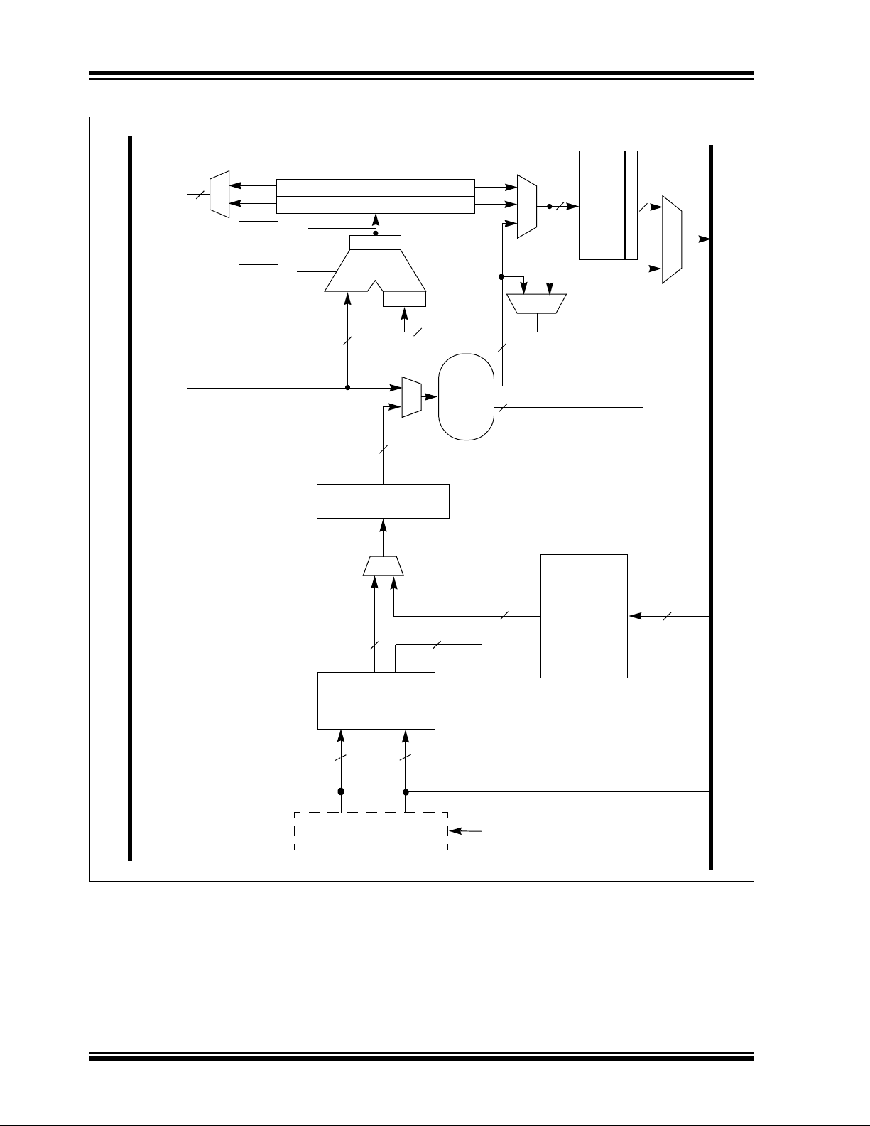
dsPIC33FJXXXGPX06/X08/X10
Zero Backfill
Sign-Extend
Barrel
Shifter
40-bit Accumulator A
40-bit Accumulator B
Round
Logic
X Data Bus
To/From W Array
Adder
Saturate
Negate
32
32
33
16
16
16
16
40
40
40
40
S
a
t
u
r
a
t
e
Y Data Bus
40
Carry/Borrow Out
Carry/Borrow In
16
40
Multiplier/Scaler
17-bit
FIGURE 3-3: DSP ENGINE BLOCK DIAGRAM
DS70286C-page 28 © 2009 Microchip Technology Inc.

dsPIC33FJXXXGPX06/X08/X10
3.6.1 MULTIPLIER
The 17-bit x 17-bit multiplier is capable of signed or
unsigned operation and can multiplex its output using a
scaler to support either 1.31 fractional (Q31) or 32-bit
integer results. Unsigned operands are zero-extended
into the 17th bit of the multiplier input value. Signed
operands are sign-extended into the 17th bit of the
multiplier input value. The output of the 17-bit x 17-bit
multiplier/scaler is a 33-bit value which is
sign-extended to 40 bits. Integer data is inherently
represented as a signed two’s complement value,
where the Most Significant bit (MSb) is defined as a
sign bit. Generally speaking, the range of an N-bit two’s
complement integer is -2
integer, the data range is -32768 (0x8000) to 32767
(0x7FFF) including 0. For a 32-bit integer, the data
range is -2,147,483,648 (0x8000 0000) to
2,147,483,647 (0x7FFF FFFF).
When the multiplier is configured for fractional
multiplication, the data is represented as a two’s
complement fraction, where the MSb is defined as a
sign bit and the radix point is implied to lie just after the
sign bit (QX format). The range of an N-bit two’s
complement fraction with this implied radix point is -1.0
1-N
to (1 - 2
-1.0 (0x8000) to 0.999969482 (0x7FFF) including 0
and has a precision of 3.01518x10
mode, the 16 x 16 multiply operation generates a 1.31
product which has a precision of 4.65661 x 10
The same multiplier is used to support the MCU
multiply instructions which include integer 16-bit
signed, unsigned and mixed sign multiplies.
The MUL instruction may be directed to use byte or
word sized operands. Byte operands will direct a 16-bit
result, and word operands will direct a 32-bit result to
the specified register(s) in the W array.
). For a 16-bit fraction, the Q15 data range is
N-1
to 2
N-1
- 1. For a 16-bit
-5
. In Fractional
-10
.
3.6.2 DATA ACCUMULATORS AND ADDER/SUBTRACTER
The data accumulator consists of a 40-bit
adder/subtracter with automatic sign extension logic. It
can select one of two accumulators (A or B) as its
pre-accumulation source and post-accumulation
destination. For the ADD and LAC instructions, the data
to be accumulated or loaded can be optionally scaled
via the barrel shifter prior to accumulation.
3.6.2.1 Adder/Subtracter, Overflow and
Saturation
The adder/subtracter is a 40-bit adder with an optional
zero input into one side, and either true, or complement
data into the other input. In the case of addition, the
Carry/Borrow
true data (not complemented), whereas in the case of
subtraction, the Carry/Borrow
the other input is complemented. The adder/subtracter
generates Overflow Status bits, SA/SB and OA/OB,
which are latched and reflected in the STATUS
register:
• Overflow from bit 39: this is a catastrophic
overflow in which the sign of the accumulator is
destroyed.
• Overflow into guard bits 32 through 39: this is a
recoverable overflow. This bit is set whenever all
the guard bits are not identical to each other.
The adder has an additional saturation block which
controls accumulator data saturation, if selected. It
uses the result of the adder, the Overflow Status bits
described above and the SAT<A:B> (CORCON<7:6>)
and ACCSAT (CORCON<4>) mode control bits to
determine when and to what value to saturate.
Six STATUS register bits have been provided to
support saturation and overflow; they are:
1. OA:
AccA overflowed into guard bits
2. OB:
AccB overflowed into guard bits
3. SA:
AccA saturated (bit 31 overflow and saturation)
or
AccA overflowed into guard bits and saturated
(bit 39 overflow and saturation)
4. SB:
AccB saturated (bit 31 overflow and saturation)
or
AccB overflowed into guard bits and saturated
(bit 39 overflow and saturation)
5. OAB:
Logical OR of OA and OB
6. SAB:
Logical OR of SA and SB
The OA and OB bits are modified each time data
passes through the adder/subtracter. When set, they
indicate that the most recent operation has overflowed
into the accumulator guard bits (bits 32 through 39).
The OA and OB bits can also optionally generate an
arithmetic warning trap when set and the
corresponding Overflow Trap Flag Enable bits (OVATE,
OVBTE) in the INTCON1 register (refer to Section 7.0
“Interrupt Controller”) are set. This allows the user to
take immediate action, for example, to correct system
gain.
input is active-high and the other input is
input is active-low and
© 2009 Microchip Technology Inc. DS70286C-page 29

dsPIC33FJXXXGPX06/X08/X10
The SA and SB bits are modified each time data
passes through the adder/subtracter, but can only be
cleared by the user. When set, they indicate that the
accumulator has overflowed its maximum range (bit 31
for 32-bit saturation or bit 39 for 40-bit saturation) and
will be saturated (if saturation is enabled). When
saturation is not enabled, SA and SB default to bit 39
overflow and, thus, indicate that a catastrophic
overflow has occurred. If the COVTE bit in the
INTCON1 register is set, SA and SB bits will generate
an arithmetic warning trap when saturation is disabled.
The Overflow and Saturation Status bits can optionally
be viewed in the STATUS Register (SR) as the logical
OR of OA and OB (in bit OAB) and the logical OR of SA
and SB (in bit SAB). This allows programmers to check
one bit in the STATUS register to determine if either
accumulator has overflowed, or one bit to determine if
either accumulator has saturated. This would be useful
for complex number arithmetic which typically uses
both the accumulators.
The device supports three Saturation and Overflow
modes:
1. Bit 39 Overflow and Saturation:
When bit 39 overflow and saturation occurs, the
saturation logic loads the maximally positive 9.31
(0x7FFFFFFFFF), or maximally negative 9.31
value (0x8000000000), into the target
accumulator. The SA or SB bit is set and remains
set until cleared by the user. This is referred to as
‘super saturation’ and provides protection against
erroneous data or unexpected algorithm
problems (e.g., gain calculations).
2. Bit 31 Overflow and Saturation:
When bit 31 overflow and saturation occurs, the
saturation logic then loads the maximally
positive 1.31 value (0x007FFFFFFF), or
maximally negative 1.31 value (0x0080000000),
into the target accumulator. The SA or SB bit is
set and remains set until cleared by the user.
When this Saturation mode is in effect, the
guard bits are not used (so the OA, OB or OAB
bits are never set).
3. Bit 39 Catastrophic Overflow:
The bit 39 Overflow Status bit from the adder is
used to set the SA or SB bit, which remains set
until cleared by the user. No saturation operation
is performed and the accumulator is allowed to
overflow (destroying its sign). If the COVTE bit in
the INTCON1 register is set, a catastrophic
overflow can initiate a trap exception.
3.6.2.2 Accumulator ‘Write Back’
The MAC class of instructions (with the exception of
MPY, MPY.N, ED and EDAC) can optionally write a
rounded version of the high word (bits 31 through 16)
of the accumulator that is not targeted by the instruction
into data space memory. The write is performed across
the X bus into combined X and Y address space. The
following addressing modes are supported:
1. W13, Register Direct:
The rounded contents of the non-target
accumulator are written into W13 as a
1.15 fraction.
2. [W13]+ = 2, Register Indirect with Post-Increment:
The rounded contents of the non-target
accumulator are written into the address pointed
to by W13 as a 1.15 fraction. W13 is then
incremented by 2 (for a word write).
3.6.2.3 Round Logic
The round logic is a combinational block which
performs a conventional (biased) or convergent
(unbiased) round function during an accumulator write
(store). The Round mode is determined by the state of
the RND bit in the CORCON register. It generates a
16-bit, 1.15 data value which is passed to the data
space write saturation logic. If rounding is not indicated
by the instruction, a truncated 1.15 data value is stored
and the least significant word is simply discarded.
Conventional rounding zero-extends bit 15 of the
accumulator and adds it to the ACCxH word (bits 16
through 31 of the accumulator). If the ACCxL word
(bits 0 through 15 of the accumulator) is between
0x8000 and 0xFFFF (0x8000 included), ACCxH is
incremented. If ACCxL is between 0x0000 and 0x7FFF,
ACCxH is left unchanged. A consequence of this
algorithm is that over a succession of random rounding
operations, the value tends to be biased slightly
positive.
Convergent (or unbiased) rounding operates in the
same manner as conventional rounding, except when
ACCxL equals 0x8000. In this case, the Least
Significant bit (bit 16 of the accumulator) of ACCxH is
examined. If it is ‘1’, ACCxH is incremented. If it is ‘0’,
ACCxH is not modified. Assuming that bit 16 is
effectively random in nature, this scheme removes any
rounding bias that may accumulate.
The SAC and SAC.R instructions store either a
truncated (SAC), or rounded (SAC.R) version of the
contents of the target accumulator to data memory via
the X bus, subject to data saturation (see
Section 3.6.2.4 “Data Space Write Saturation”). For
the MAC class of instructions, the accumulator
write-back operation will function in the same manner,
addressing combined MCU (X and Y) data space
though the X bus. For this class of instructions, the data
is always subject to rounding.
DS70286C-page 30 © 2009 Microchip Technology Inc.

dsPIC33FJXXXGPX06/X08/X10
3.6.2.4 Data Space Write Saturation
In addition to adder/subtracter saturation, writes to data
space can also be saturated but without affecting the
contents of the source accumulator. The data space
write saturation logic block accepts a 16-bit, 1.15
fractional value from the round logic block as its input,
together with overflow status from the original source
(accumulator) and the 16-bit round adder. These inputs
are combined and used to select the appropriate 1.15
fractional value as output to write to data space
memory.
If the SATDW bit in the CORCON register is set, data
(after rounding or truncation) is tested for overflow and
adjusted accordingly, For input data greater than
0x007FFF, data written to memory is forced to the
maximum positive 1.15 value, 0x7FFF. For input data
less than 0xFF8000, data written to memory is forced
to the maximum negative 1.15 value, 0x8000. The
Most Significant bit of the source (bit 39) is used to
determine the sign of the operand being tested.
If the SATDW bit in the CORCON register is not set, the
input data is always passed through unmodified under
all conditions.
3.6.3 BARREL SHIFTER
The barrel shifter is capable of performing up to 16-bit
arithmetic or logic right shifts, or up to 16-bit left shifts
in a single cycle. The source can be either of the two
DSP accumulators or the X bus (to support multi-bit
shifts of register or memory data).
The shifter requires a signed binary value to determine
both the magnitude (number of bits) and direction of the
shift operation. A positive value shifts the operand right.
A negative value shifts the operand left. A value of ‘0’
does not modify the operand.
The barrel shifter is 40 bits wide, thereby obtaining a
40-bit result for DSP shift operations and a 16-bit result
for MCU shift operations. Data from the X bus is
presented to the barrel shifter between bit positions 16
to 31 for right shifts, and between bit positions 0 to 16
for left shifts.
© 2009 Microchip Technology Inc. DS70286C-page 31

dsPIC33FJXXXGPX06/X08/X10
NOTES:
DS70286C-page 32 © 2009 Microchip Technology Inc.

dsPIC33FJXXXGPX06/X08/X10
Reset Address
0x000000
0x0000FE
0x000002
0x000100
Device Configuration
User Program
Flash Memory
0x00AC00
0x00ABFE
(22K instructions)
0x800000
0xF80000
Registers
0xF80017
0xF80010
DEVID (2)
0xFEFFFE
0xFF0000
0xFFFFFE
0xF7FFFE
Unimplemented
(Read ‘0’s)
GOTO Instruction
0x000004
Reserved
0x7FFFFE
Reserved
0x000200
0x0001FE
0x000104
Alternate Vector Table
Reserved
Interrupt Vector Table
Reset Address
Device Configuration
Registers
DEVID (2)
Unimplemented
(Read ‘0’s)
GOTO
Instruction
Reserved
Reserved
Alternate Vector Table
Reserved
Interrupt Vector Table
Reset Address
Device Configuration
User Program
Flash Memory
(88K instructions)
Registers
DEVID (2)
GOTO
Instruction
Reserved
Reserved
Alternate Vector Table
Reserved
Interrupt Vector Table
dsPIC33FJ64GPXXX dsPIC33FJ128GPXXX dsPIC33FJ256GPXXX
Configuration Memory Space
User Memory Space
0x015800
0x0157FE
Note: Memory areas are not shown to scale.
User Program
(44K instructions)
Flash Memory
(Read ‘0’s)
Unimplemented
0x02AC00
0x02ABFE
4.0 MEMORY ORGANIZATION
Note: This data sheet summarizes the features
of the dsPIC33FJXXXGPX06/X08/X10
family of devices. However, it is not
intended to be a comprehensive reference
source. To complement the information in
this data sheet, refer to Section 3. “Data
Memory” (DS70202) and Section 4.
“Program Memory” (DS70203) in the
“dsPIC33F Family Reference Manual”,
which is available from the Microchip web
site (www.microchip.com).
The dsPIC33FJXXXGPX06/X08/X10 architecture
features separate program and data memory spaces
and buses. This architecture also allows the direct
access of program memory from the data space during
4.1 Program Address Space
The program address memory space of the
dsPIC33FJXXXGPX06/X08/X10 devices is 4M
instructions. The space is addressable by a 24-bit
value derived from either the 23-bit Program Counter
(PC) during program execution, or from table operation
or data space remapping as described in Section 4.6
“Interfacing Program and Data Memory Spaces”.
User access to the program memory space is restricted
to the lower half of the address range (0x000000 to
0x7FFFFF). The exception is the use of TBLRD/TBLWT
operations, which use TBLPAG<7> to permit access to
the Configuration bits and Device ID sections of the
configuration memory space. Memory usage for the
dsPIC33FJXXXGPX06/X08/X10 of devices is shown in
Figure 4-1.
code execution.
FIGURE 4-1: PROGRAM MEMORY FOR dsPIC33FJXXXGPX06/X08/X10 DEVICES
© 2009 Microchip Technology Inc. DS70286C-page 33
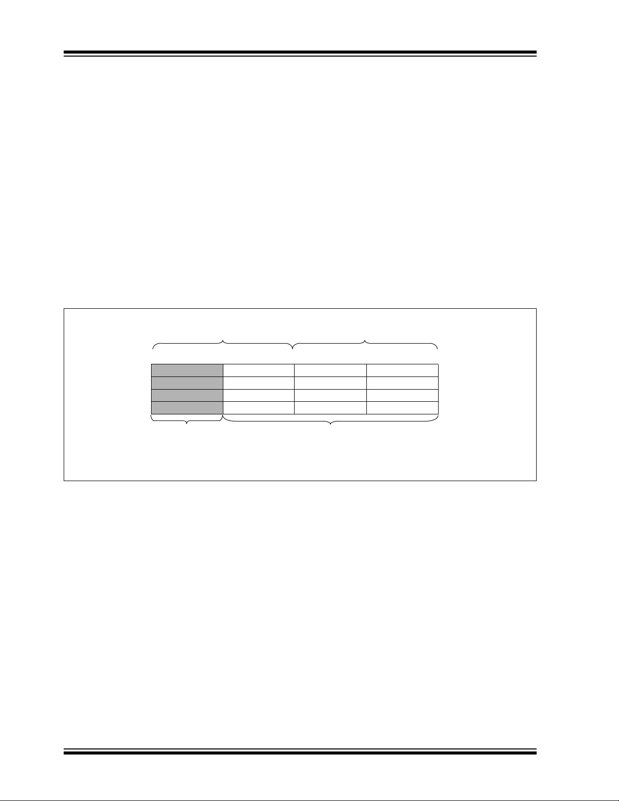
dsPIC33FJXXXGPX06/X08/X10
0816
PC Address
0x000000
0x000002
0x000004
0x000006
23
00000000
00000000
00000000
00000000
Program Memory
‘Phantom’ Byte
(read as ‘0’)
least significant word
most significant word
Instruction Width
0x000001
0x000003
0x000005
0x000007
msw
Address (lsw Address)
4.1.1 PROGRAM MEMORY ORGANIZATION
The program memory space is organized in
word-addressable blocks. Although it is treated as
24 bits wide, it is more appropriate to think of each
address of the program memory as a lower and upper
word, with the upper byte of the upper word being
unimplemented. The lower word always has an even
address, while the upper word has an odd address
(Figure 4-2).
Program memory addresses are always word-aligned
on the lower word, and addresses are incremented or
decremented by two during code execution. This
arrangement also provides compatibility with data
memory space addressing and makes it possible to
access data in the program memory space.
4.1.2 INTERRUPT AND TRAP VECTORS
All dsPIC33FJXXXGPX06/X08/X10 devices reserve
the addresses between 0x00000 and 0x000200 for
hard-coded program execution vectors. A hardware
Reset vector is provided to redirect code execution
from the default value of the PC on device Reset to the
actual start of code. A GOTO instruction is programmed
by the user at 0x000000, with the actual address for the
start of code at 0x000002.
dsPIC33FJXXXGPX06/X08/X10 devices also have
two interrupt vector tables, located from 0x000004 to
0x0000FF and 0x000100 to 0x0001FF. These vector
tables allow each of the many device interrupt sources
to be handled by separate Interrupt Service Routines
(ISRs). A more detailed discussion of the interrupt
vector tables is provided in Section 7.1 “Interrupt
Vector Table”.
FIGURE 4-2: PROGRAM MEMORY ORGANIZATION
DS70286C-page 34 © 2009 Microchip Technology Inc.

dsPIC33FJXXXGPX06/X08/X10
4.2 Data Address Space
The dsPIC33FJXXXGPX06/X08/X10 CPU has a
separate 16-bit wide data memory space. The data
space is accessed using separate Address Generation
Units (AGUs) for read and write operations. Data
memory maps of devices with different RAM sizes are
shown in Figure 4-3 through Figure 4-5.
All Effective Addresses (EAs) in the data memory space
are 16 bits wide and point to bytes within the data space.
This arrangement gives a data space address range of
64 Kbytes or 32K words. The lower half of the data
memory space (that is, when EA<15> = 0) is used for
implemented memory addresses, while the upper half
(EA<15> = 1) is reserved for the Program Space
Visibility area (see Section 4.6.3 “Reading Data from
Program Memory Using Program Space Visibility”).
dsPIC33FJXXXGPX06/X08/X10 devices implement a
total of up to 30 Kbytes of data memory. Should an EA
point to a location outside of this area, an all-zero word
or byte will be returned.
4.2.1 DATA SPACE WIDTH
The data memory space is organized in byte
addressable, 16-bit wide blocks. Data is aligned in data
memory and registers as 16-bit words, but all data
space EAs resolve to bytes. The Least Significant
Bytes (LSBs) of each word have even addresses, while
the Most Significant Bytes (MSBs) have odd
addresses.
4.2.2 DATA MEMORY ORGANIZATION AND ALIGNMENT
To maintain backward compatibility with PIC
devices and improve data space memory usage
efficiency, the dsPIC33FJXXXGPX06/X08/X10
instruction set supports both word and byte operations.
As a consequence of byte accessibility, all effective
address calculations are internally scaled to step
through word-aligned memory. For example, the core
recognizes that Post-Modified Register Indirect
Addressing mode [Ws++] will result in a value of Ws + 1
for byte operations and Ws + 2 for word operations.
Data byte reads will read the complete word that
contains the byte, using the LSb of any EA to determine
which byte to select. The selected byte is placed onto
the LSb of the data path. That is, data memory and
registers are organized as two parallel byte-wide
entities with shared (word) address decode but
separate write lines. Data byte writes only write to the
corresponding side of the array or register which
matches the byte address.
®
MCU
All word accesses must be aligned to an even address.
Misaligned word data fetches are not supported, so
care must be taken when mixing byte and word
operations, or translating from 8-bit MCU code. If a
misaligned read or write is attempted, an address error
trap is generated. If the error occurred on a read, the
instruction underway is completed; if it occurred on a
write, the instruction will be executed but the write does
not occur. In either case, a trap is then executed,
allowing the system and/or user to examine the
machine state prior to execution of the address Fault.
All byte loads into any W register are loaded into the
Least Significant Byte. The Most Significant Byte is not
modified.
A sign-extend instruction (SE) is provided to allow
users to translate 8-bit signed data to 16-bit signed
values. Alternatively, for 16-bit unsigned data, users
can clear the MSb of any W register by executing a
zero-extend (ZE) instruction on the appropriate
address.
4.2.3 SFR SPACE
The first 2 Kbytes of the Near Data Space, from 0x0000
to 0x07FF, is primarily occupied by Special Function
Registers (SFRs). These are used by the
dsPIC33FJXXXGPX06/X08/X10 core and peripheral
modules for controlling the operation of the device.
SFRs are distributed among the modules that they
control, and are generally grouped together by module.
Much of the SFR space contains unused addresses;
these are read as ‘0’. A complete listing of implemented
SFRs, including their addresses, is shown in Table 4-1
through Table 4-34.
Note: The actual set of peripheral features and
interrupts varies by the device. Please
refer to the corresponding device tables
and pinout diagrams for device-specific
information.
4.2.4 NEAR DATA SPACE
The 8-Kbyte area between 0x0000 and 0x1FFF is
referred to as the Near Data Space. Locations in this
space are directly addressable via a 13-bit absolute
address field within all memory direct instructions.
Additionally, the whole data space is addressable using
MOV instructions, which support Memory Direct
Addressing mode with a 16-bit address field, or by
using Indirect Addressing mode using a working
register as an Address Pointer.
© 2009 Microchip Technology Inc. DS70286C-page 35
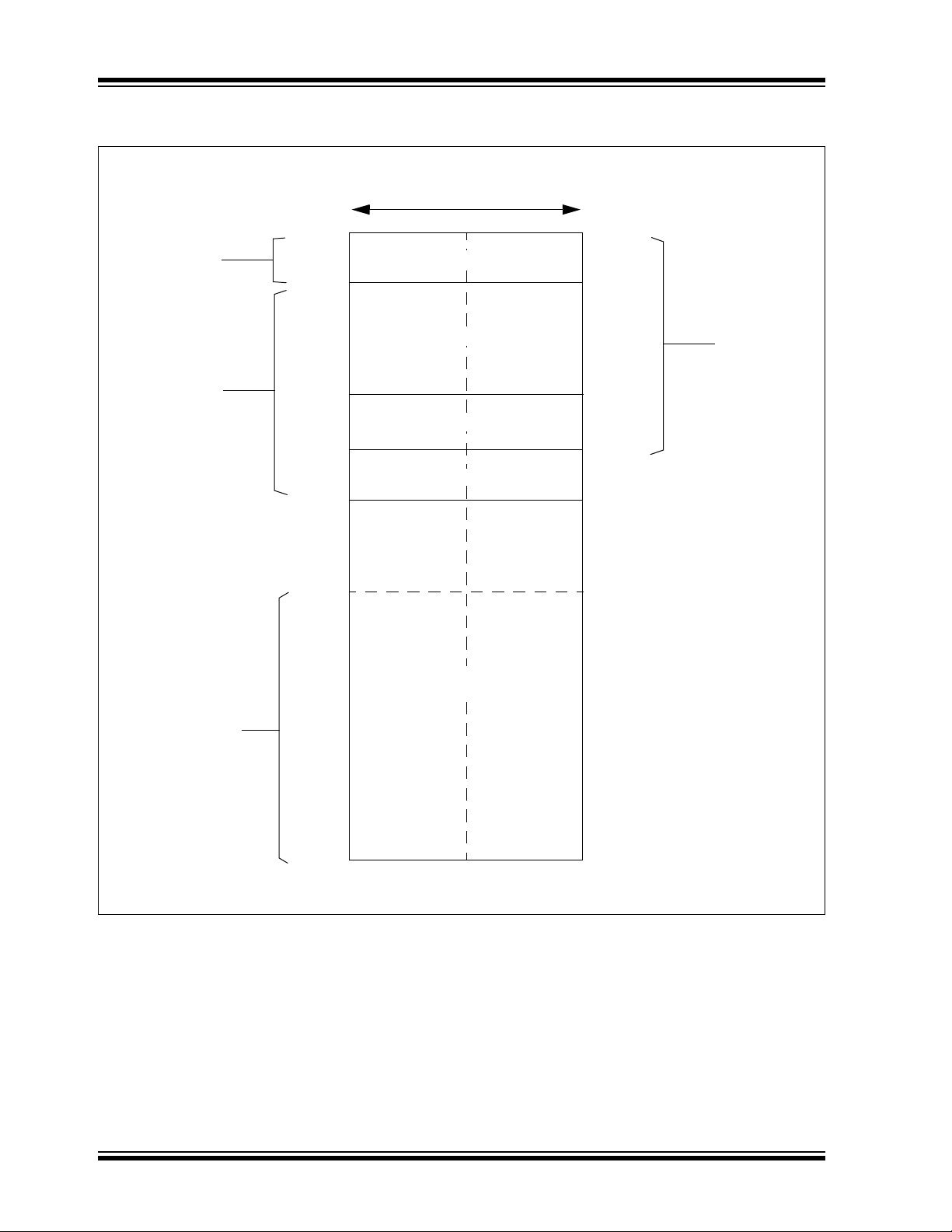
dsPIC33FJXXXGPX06/X08/X10
0x0000
0x07FE
0x17FE
0xFFFE
LSB
Address
16 bits
LSBMSB
MSB
Address
0x0001
0x07FF
0x17FF
0xFFFF
Optionally
Mapped
into Program
Memory
0x27FF 0x27FE
0x0801
0x0800
0x1801
0x1800
2 Kbyte
SFR Space
8 Kbyte
SRAM Space
0x8001
0x8000
0x28000x2801
0x1FFE
0x2000
0x1FFF
0x2001
Space
Data
Near
8 Kbyte
SFR Space
X Data RAM (X)
X Data
Unimplemented (X)
DMA RAM
Y Data RAM (Y)
FIGURE 4-3: DATA MEMORY MAP FOR dsPIC33FJXXXGPX06/X08/X10 DEVICES WITH 8 KBS
RAM
DS70286C-page 36 © 2009 Microchip Technology Inc.

dsPIC33FJXXXGPX06/X08/X10
0x0000
0x07FE
0x27FE
0xFFFE
LSB
Address
16 bits
LSBMSB
MSB
Address
0x0001
0x07FF
0x27FF
0xFFFF
Optionally
Mapped
into Program
Memory
0x47FF 0x47FE
0x0801
0x0800
0x2801
0x2800
Near
Data
2 Kbyte
SFR Space
16 Kbyte
SRAM Space
8 Kbyte
Space
0x8001
0x8000
0x48000x4801
0x3FFE
0x4000
0x3FFF
0x4001
0x1FFE
0x1FFF
SFR Space
X Data RAM (X)
X Data
Unimplemented (X)
DMA RAM
Y Data RAM (Y)
FIGURE 4-4: DATA MEMORY MAP FOR dsPIC33FJXXXGPX06/X08/X10 DEVICES WITH 16 KB
RAM
© 2009 Microchip Technology Inc. DS70286C-page 37

dsPIC33FJXXXGPX06/X08/X10
0x0000
0x07FE
SFR Space
0xFFFE
X Data RAM (X)
16 bits
LSBMSB
0x0001
0x07FF
0xFFFF
X Data
Optionally
Mapped
into Program
Memory
Unimplemented (X)
0x0801
0x0800
2 Kbyte
SFR Space
0x4800
0x47FE
0x4801
0x47FF
0x7FFE
0x8000
30 Kbyte
SRAM Space
0x7FFF
0x8001
Y Data RAM (Y)
Near
Data
8 Kbyte
Space
0x77FE
0x7800
0x77FF
0x7800
LSB
Address
MSB
Address
DMA RAM
FIGURE 4-5: DATA MEMORY MAP FOR dsPIC33FJXXXGPX06/X08/X10 DEVICES WITH 30 KB
RAM
DS70286C-page 38 © 2009 Microchip Technology Inc.

dsPIC33FJXXXGPX06/X08/X10
4.2.5 X AND Y DATA SPACES
The core has two data spaces, X and Y. These data
spaces can be considered either separate (for some
DSP instructions), or as one unified linear address
range (for MCU instructions). The data spaces are
accessed using two Address Generation Units (AGUs)
and separate data paths. This feature allows certain
instructions to concurrently fetch two words from RAM,
thereby enabling efficient execution of DSP algorithms
such as Finite Impulse Response (FIR) filtering and
Fast Fourier Transform (FFT).
The X data space is used by all instructions and
supports all addressing modes. There are separate
read and write data buses for X data space. The X read
data bus is the read data path for all instructions that
view data space as combined X and Y address space.
It is also the X data prefetch path for the dual operand
DSP instructions (MAC class).
The Y data space is used in concert with the X data
space by the MAC class of instructions (CLR, ED,
EDAC, MAC, MOVSAC, MPY, MPY.N and MSC) to provide
two concurrent data read paths.
Both the X and Y data spaces support Modulo
Addressing mode for all instructions, subject to
addressing mode restrictions. Bit-Reversed Addressing
mode is only supported for writes to X data space.
All data memory writes, including in DSP instructions,
view data space as combined X and Y address space.
The boundary between the X and Y data spaces is
device-dependent and is not user-programmable.
All effective addresses are 16 bits wide and point to
bytes within the data space. Therefore, the data space
address range is 64 Kbytes, or 32K words, though the
implemented memory locations vary by device.
4.2.6 DMA RAM
Every dsPIC33FJXXXGPX06/X08/X10 device contains
2 Kbytes of dual ported DMA RAM located at the end of
Y data space. Memory locations is part of Y data RAM
and is in the DMA RAM space are accessible
simultaneously by the CPU and the DMA controller
module. DMA RAM is utilized by the DMA controller to
store data to be transferred to various peripherals using
DMA, as well as data transferred from various
peripherals using DMA. The DMA RAM can be
accessed by the DMA controller without having to steal
cycles from the CPU.
When the CPU and the DMA controller attempt to
concurrently write to the same DMA RAM location, the
hardware ensures that the CPU is given precedence in
accessing the DMA RAM location. Therefore, the DMA
RAM provides a reliable means of transferring DMA
data without ever having to stall the CPU.
Note: DMA RAM can be used for general
purpose data storage if the DMA function
is not required in an application.
© 2009 Microchip Technology Inc. DS70286C-page 39

DS70286C-page 40 © 2009 Microchip Technology Inc.
TABLE 4-1: CPU CORE REGISTERS MAP
SFR Name
WREG0 0000 Working Register 0
WREG1 0002 Working Register 1
WREG2 0004 Working Register 2
WREG3 0006 Working Register 3
WREG4 0008 Working Register 4
WREG5 000A Working Register 5
WREG6 000C Working Register 6
WREG7 000E Working Register 7
WREG8 0010 Working Register 8
WREG9 0012 Working Register 9
WREG10 0014 Working Register 10
WREG11 0016 Working Register 11
WREG12 0018 Working Register 12
WREG13 001A Working Register 13
WREG14 001C Working Register 14
WREG15 001E Working Register 15
SPLIM 0020 Stack Pointer Limit Register
ACCAL 0022 Accumulator A Low Word Register
ACCAH 0024 Accumulator A High Word Register
ACCAU 0026 Accumulator A Upper Word Register
ACCBL 0028 Accumulator B Low Word Register
ACCBH 002A Accumulator B High Word Register
ACCBU 002C Accumulator B Upper Word Register
PCL 002E Program Counter Low Word Register
PCH 0030 — — — — — — — — Program Counter High Byte Register
TBLPAG 0032 — — — — — — — — Table Page Address Pointer Register
PSVPAG 0034 — — — — — — — — Program Memory Visibility Page Address Pointer Register
RCOUNT 0036 Repeat Loop Counter Register
DCOUNT 0038 DCOUNT<15:0> xxxx
DOSTARTL 003A DOSTARTL<15:1> 0xxxx
DOSTARTH 003C
DOENDL 003E DOENDL<15:1> 0xxxx
DOENDH 0040
SR 0042 OA OB SA SB OAB SAB DA DC IPL2 IPL1 IPL0 RA N OV Z C
CORCON 0044 — — —USEDT DL<2:0>
MODCON 0046 XMODEN YMODEN
XMODSRT 0048 XS<15:1> 0xxxx
XMODEND 004A XE<15:1> 1xxxx
YMODSRT 004C YS<15:1> 0xxxx
YMODEND 004E YE<15:1> 1xxxx
Legend: x = unknown value on Reset, — = unimplemented, read as ‘0’. Reset values are shown in hexadecimal.
SFR
Addr
Bit 15 Bit 14 Bit 13 Bit 12 Bit 11 Bit 10 Bit 9 Bit 8 Bit 7 Bit 6 Bit 5 Bit 4 Bit 3 Bit 2 Bit 1 Bit 0
— — — — — — — — — —
— — — — — — — — — —
SATA SATB SATDW ACCSAT IPL3 PSV RND IF
— —
BWM<3:0> YWM<3:0> XWM<3:0> 0000
DOSTARTH<5:0> 00xx
DOENDH 00xx
All
Resets
0000
0000
0000
0000
0000
0000
0000
0000
0000
0000
0000
0000
0000
0000
0000
0800
xxxx
0000
0000
0000
0000
0000
0000
0000
0000
0000
0000
xxxx
0000
0020
dsPIC33FJXXXGPX06/X08/X10

© 2009 Microchip Technology Inc. DS70286C-page 41
TABLE 4-1: CPU CORE REGISTERS MAP (CONTINUED)
SFR Name
XBREV 0050 BREN XB<14:0> xxxx
DISICNT 0052 —
BSRAM 0750
SSRAM 0752
Legend: x = unknown value on Reset, — = unimplemented, read as ‘0’. Reset values are shown in hexadecimal.
SFR
Addr
Bit 15 Bit 14 Bit 13 Bit 12 Bit 11 Bit 10 Bit 9 Bit 8 Bit 7 Bit 6 Bit 5 Bit 4 Bit 3 Bit 2 Bit 1 Bit 0
— Disable Interrupts Counter
— — — — — — — — — — — — —
— — — — — — — — — — — — —
Register
IW_BSR IR_BSR RL_BSR
IW_SSR IR_SSR RL_SSR
Resets
xxxx
0000
0000
All
dsPIC33FJXXXGPX06/X08/X10
DS70286C-page 42 © 2009 Microchip Technology Inc.
TABLE 4-2: CHANGE NOTIFICATION REGISTER MAP FOR dsPIC33FJXXXGPX10 DEVICES
SFR
Name
CNEN1 0060 CN15IE CN14IE CN13IE CN12IE CN11IE CN10IE CN9IE CN8IE CN7IE CN6IE CN5IE CN4IE CN3IE CN2IE CN1IE CN0IE
CNEN2 0062
CNPU1 0068 CN15PUE CN14PUE CN13PUE CN12PUE CN11PUE CN10PUE CN9PUE CN8PUE CN7PUE CN6PUE CN5PUE CN4PUE CN3PUE CN2PUE CN1PUE CN0PUE
CNPU2 006A
Legend: x = unknown value on Reset, — = unimplemented, read as ‘0’. Reset values are shown in hexadecimal.
SFR
Addr
Bit 15Bit 14Bit 13Bit 12Bit 11Bit 10Bit 9Bit 8Bit 7Bit 6Bit 5Bit 4Bit 3Bit 2Bit 1Bit 0
— — — — — — — —
— — — — — — — —
CN23IE CN22IE CN21IE CN20IE CN19IE CN18IE CN17IE CN16IE
CN23PUE CN22PUE CN21PUE CN20PUE CN19PUE CN18PUE CN17PUE CN16PUE
TABLE 4-3: CHANGE NOTIFICATION REGISTER MAP FOR dsPIC33FJXXXGPX08 DEVICES
SFR
Name
CNEN1 0060 CN15IE CN14IE CN13IE CN12IE CN11IE CN10IE CN9IE CN8IE CN7IE CN6IE CN5IE CN4IE CN3IE CN2IE CN1IE CN0IE
CNEN2 0062
CNPU1 0068 CN15PUE CN14PUE CN13PUE CN12PUE CN11PUE CN10PUE CN9PUE CN8PUE CN7PUE CN6PUE CN5PUE CN4PUE CN3PUE CN2PUE CN1PUE CN0PUE
CNPU2 006A
Legend: x = unknown value on Reset, — = unimplemented, read as ‘0’. Reset values are shown in hexadecimal.
SFR
Addr
Bit 15Bit 14Bit 13Bit 12Bit 11Bit 10Bit 9Bit 8Bit 7Bit 6Bit 5Bit 4Bit 3Bit 2Bit 1Bit 0
— — — — — — — — — —
— — — — — — — — — —
CN21IE CN20IE CN19IE CN18IE CN17IE CN16IE
CN21PUE CN20PUE CN19PUE CN18PUE CN17PUE CN16PUE
TABLE 4-4: CHANGE NOTIFICATION REGISTER MAP FOR dsPIC33FJXXXGPX06 DEVICES
SFR
Name
CNEN1 0060 CN15IE CN14IE CN13IE CN12IE CN11IE CN10IE CN9IE CN8IE CN7IE CN6IE CN5IE CN4IE CN3IE CN2IE CN1IE CN0IE
CNEN2 0062
CNPU1 0068 CN15PUE CN14PUE CN13PUE CN12PUE CN11PUE CN10PUE CN9PUE CN8PUE CN7PUE CN6PUE CN5PUE CN4PUE CN3PUE CN2PUE CN1PUE CN0PUE
CNPU2 006A
Legend: x = unknown value on Reset, — = unimplemented, read as ‘0’. Reset values are shown in hexadecimal.
SFR
Addr
Bit 15Bit 14Bit 13Bit 12Bit 11Bit 10Bit 9Bit 8Bit 7Bit 6Bit 5Bit 4Bit 3Bit 2Bit 1Bit 0
— — — — — — — — — —
— — — — — — — — — —
CN21IE CN20IE — CN18IE CN17IE CN16IE
CN21PUE CN20PUE — CN18PUE CN17PUE CN16PUE
All
Resets
0000
0000
0000
0000
All
Resets
0000
0000
0000
0000
All
Resets
0000
0000
0000
0000
dsPIC33FJXXXGPX06/X08/X10

© 2009 Microchip Technology Inc. DS70286C-page 43
TABLE 4-5: INTERRUPT CONTROLLER REGISTER MAP
SFR
Name
INTCON1 0080 NSTDIS OVAERR OVBERR COVAERR COVBERR OVATE OVBTE COVTE SFTACERR DIV0ERR DMACERR MATHERR ADDRERR STKERR OSCFAIL
INTCON2 0082 ALTIVT DISI
IFS0 0084
IFS1 0086 U2TXIF U2RXIF INT2IF T5IF T4IF OC4IF OC3IF DMA2IF IC8IF IC7IF AD2IF INT1IF CNIF
IFS2 0088 T6IF DMA4IF
IFS3 008A
IFS4 008C
IEC0 0094
IEC1 0096 U2TXIE U2RXIE INT2IE T5IE T4IE OC4IE OC3IE DMA2IE IC8IE IC7IE AD2IE INT1IE CNIE
IEC2 0098 T6IE DMA4IE
IEC3 009A
IEC4 009C
IPC0 00A4
IPC1 00A6
IPC2 00A8
IPC3 00AA
IPC4 00AC
IPC5 00AE
IPC6 00B0
IPC7 00B2
IPC8 00B4
IPC9 00B6
IPC10 00B8
IPC11 00BA
IPC12 00BC
IPC13 00BE
IPC14 00C0
IPC15 00C2
IPC16 00C4
IPC17 00C6
INTTREG 00E0
Legend: x = unknown value on Reset, — = unimplemented, read as ‘0’. Reset values are shown in hexadecimal.
SFR
Bit 15 Bit 14 Bit 13 Bit 12 Bit 11 Bit 10 Bit 9 Bit 8 Bit 7 Bit 6 Bit 5 Bit 4 Bit 3 Bit 2 Bit 1 Bit 0
Addr
— — — — — — — — — INT4EP INT3EP INT2EP INT1EP INT0EP 0000
— DMA1IF AD1IF U1TXIF U1RXIF SPI1IF SPI1EIF T3IF T2IF OC2IF IC2IF DMA0IF T1IF OC1IF IC1IF INT0IF 0000
— MI2C1IF SI2C1IF 0000
— OC8IF OC7IF OC6IF OC5IF IC6IF IC5IF IC4IF IC3IF DMA3IF C1IF C1RXIF SPI2IF SPI2EIF 0000
— — DMA5IF DCIIF DCIEIF — — C2IF C2RXIF INT4IF INT3IF T9IF T8IF MI2C2IF SI2C2IF T7IF 0000
— — — — — — — — C2TXIF C1TXIF DMA7IF DMA6IF —U2EIFU1EIF— 0000
— DMA1IE AD1IE U1TXIE U1RXIE SPI1IE SPI1EIE T3IE T2IE OC2IE IC2IE DMA0IE T1IE OC1IE IC1IE INT0IE 0000
— MI2C1IE SI2C1IE 0000
— OC8IE OC7IE OC6IE OC5IE IC6IE IC5IE IC4IE IC3IE DMA3IE C1IE C1RXIE SPI2IE SPI2EIE 0000
— — DMA5IE DCIIE DCIEIE — — C2IE C2RXIE INT4IE INT3IE T9IE T8IE MI2C2IE SI2C2IE T7IE 0000
— — — — — — — — C2TXIE C1TXIE DMA7IE DMA6IE —U2EIEU1EIE— 0000
— T1IP<2:0> — OC1IP<2:0> —IC1IP<2:0>— INT0IP<2:0> 4444
— T2IP<2:0> — OC2IP<2:0> —IC2IP<2:0>— DMA0IP<2:0> 4444
— U1RXIP<2:0> — SPI1IP<2:0> — SPI1EIP<2:0> — T3IP<2:0> 4444
— — — — — DMA1IP<2:0> — AD1IP<2:0> — U1TXIP<2:0> 0444
— CNIP<2:0> — — — — — MI2C1IP<2:0> — SI2C1IP<2:0> 4044
— IC8IP<2:0> —IC7IP<2:0> — AD2IP<2:0> — INT1IP<2:0> 4444
— T4IP<2:0> — OC4IP<2:0> — OC3IP<2:0> — DMA2IP<2:0> 4444
— U2TXIP<2:0> — U2RXIP<2:0> — INT2IP<2:0> — T5IP<2:0> 4444
— C1IP<2:0> — C1RXIP<2:0> — SPI2IP<2:0> — SPI2EIP<2:0> 4444
— IC5IP<2:0> —IC4IP<2:0> —IC3IP<2:0>— DMA3IP<2:0> 4444
—OC7IP<2:0> — OC6IP<2:0> — OC5IP<2:0> — IC6IP<2:0> 4444
— T6IP<2:0> — DMA4IP<2:0> — — — — —OC8IP<2:0>4404
— T8IP<2:0> —MI2C2IP<2:0> — SI2C2IP<2:0> — T7IP<2:0> 4444
— C2RXIP<2:0> — INT4IP<2:0> — INT3IP<2:0> — T9IP<2:0> 4444
— DCIEIP<2:0> — — — — — — — — — C2IP<2:0> 4004
— — — — — — — — — DMA5IP<2:0> — DCIIP<2:0> 0044
— — — — — U2EIP<2:0> — U1EIP<2:0> — — — — 0440
— C2TXIP<2:0> — C1TXIP<2:0> — DMA7IP<2:0> — DMA6IP<2:0> 4444
— — — —ILR<3:0> — VECNUM<6:0> 0000
All
Resets
— 0000
dsPIC33FJXXXGPX06/X08/X10

DS70286C-page 44 © 2009 Microchip Technology Inc.
TABLE 4-6: TIMER REGISTER MAP
SFR
Name
TMR1 0100 Timer1 Register
PR1 0102 Period Register 1
T1CON 0104 TON
TMR2 0106 Timer2 Register
TMR3HLD 0108 Timer3 Holding Register (for 32-bit timer operations only)
TMR3 010A Timer3 Register
PR2 010C Period Register 2
PR3 010E Period Register 3
T2CON 0110 TON
T3CON 0112 TON
TMR4 0114 Timer4 Register
TMR5HLD 0116 Timer5 Holding Register (for 32-bit operations only)
TMR5 0118 Timer5 Register
PR4 011A Period Register 4
PR5 011C Period Register 5
T4CON 011E TON
T5CON 0120 TON
TMR6 0122 Timer6 Register
TMR7HLD 0124 Timer7 Holding Register (for 32-bit operations only)
TMR7 0126 Timer7 Register
PR6 0128 Period Register 6
PR7 012A Period Register 7
T6CON 012C TON —TSIDL— — — — — — TGATE TCKPS<1:0> T32 —TCS
T7CON 012E TON —TSIDL— — — — — — TGATE TCKPS<1:0> — —TCS
TMR8 0130 Timer8 Register
TMR9HLD 0132 Timer9 Holding Register (for 32-bit operations only)
TMR9 0134 Timer9 Register
PR8 0136 Period Register 8
PR9 0138 Period Register 9
T8CON 013A TON
T9CON 013C TON
Legend: x = unknown value on Reset, — = unimplemented, read as ‘0’. Reset values are shown in hexadecimal.
SFR
Bit 15 Bit 14 Bit 13 Bit 12 Bit 11 Bit 10 Bit 9 Bit 8 Bit 7 Bit 6 Bit 5 Bit 4 Bit 3 Bit 2 Bit 1 Bit 0
Addr
—
—
—
—
—
—
—
TSIDL
TSIDL
TSIDL
TSIDL
TSIDL
TSIDL
TSIDL
— — — — — —
— — — — — —
— — — — — —
— — — — — —
— — — — — —
— — — — — —
— — — — — —
TGATE TCKPS<1:0>
TGATE TCKPS<1:0> T32
TGATE TCKPS<1:0>
TGATE TCKPS<1:0> T32
TGATE TCKPS<1:0>
TGATE TCKPS<1:0> T32
TGATE TCKPS<1:0>
—
— —
— —
— —
TSYNC TCS
—
—
—
TCS
TCS
TCS
TCS
TCS
TCS
dsPIC33FJXXXGPX06/X08/X10
All
Resets
xxxx
FFFF
—
0000
xxxx
xxxx
xxxx
FFFF
FFFF
—
0000
—
0000
xxxx
xxxx
xxxx
FFFF
FFFF
—
0000
—
0000
xxxx
xxxx
xxxx
FFFF
FFFF
—
0000
—
0000
xxxx
xxxx
xxxx
FFFF
FFFF
—
0000
—
0000

© 2009 Microchip Technology Inc. DS70286C-page 45
TABLE 4-7: INPUT CAPTURE REGISTER MAP
SFR Name
IC1BUF 0140 Input 1 Capture Register
IC1CON 0142
IC2BUF 0144 Input 2 Capture Register
IC2CON 0146
IC3BUF 0148 Input 3 Capture Register
IC3CON 014A
IC4BUF 014C Input 4 Capture Register
IC4CON 014E
IC5BUF 0150 Input 5 Capture Register
IC5CON 0152
IC6BUF 0154 Input 6 Capture Register
IC6CON 0156
IC7BUF 0158 Input 7 Capture Register
IC7CON 015A
IC8BUF 015C Input 8 Capture Register
IC8CON 015E
Legend: x = unknown value on Reset, — = unimplemented, read as ‘0’. Reset values are shown in hexadecimal.
SFR
Addr
Bit 15 Bit 14 Bit 13 Bit 12 Bit 11 Bit 10 Bit 9 Bit 8 Bit 7 Bit 6 Bit 5 Bit 4 Bit 3 Bit 2 Bit 1 Bit 0
— —
— —
— —
— —
— —
— —
— —
— —
ICSIDL
ICSIDL
ICSIDL
ICSIDL
ICSIDL
ICSIDL
ICSIDL
ICSIDL
— — — — —
— — — — —
— — — — —
— — — — —
— — — — —
— — — — —
— — — — —
— — — — —
ICTMR ICI<1:0> ICOV ICBNE ICM<2:0>
ICTMR ICI<1:0> ICOV ICBNE ICM<2:0>
ICTMR ICI<1:0> ICOV ICBNE ICM<2:0>
ICTMR ICI<1:0> ICOV ICBNE ICM<2:0>
ICTMR ICI<1:0> ICOV ICBNE ICM<2:0>
ICTMR ICI<1:0> ICOV ICBNE ICM<2:0>
ICTMR ICI<1:0> ICOV ICBNE ICM<2:0>
ICTMR ICI<1:0> ICOV ICBNE ICM<2:0>
All
Resets
xxxx
0000
xxxx
0000
xxxx
0000
xxxx
0000
xxxx
0000
xxxx
0000
xxxx
0000
xxxx
0000
dsPIC33FJXXXGPX06/X08/X10

DS70286C-page 46 © 2009 Microchip Technology Inc.
TABLE 4-8: OUTPUT COMPARE REGISTER MAP
SFR Name
OC1RS 0180 Output Compare 1 Secondary Register
OC1R 0182 Output Compare 1 Register
OC1CON 0184
OC2RS 0186 Output Compare 2 Secondary Register
OC2R 0188 Output Compare 2 Register
OC2CON 018A
OC3RS 018C Output Compare 3 Secondary Register
OC3R 018E Output Compare 3 Register
OC3CON 0190
OC4RS 0192 Output Compare 4 Secondary Register
OC4R 0194 Output Compare 4 Register
OC4CON 0196
OC5RS 0198 Output Compare 5 Secondary Register
OC5R 019A Output Compare 5 Register
OC5CON 019C
OC6RS 019E Output Compare 6 Secondary Register
OC6R 01A0 Output Compare 6 Register
OC6CON 01A2
OC7RS 01A4 Output Compare 7 Secondary Register
OC7R 01A6 Output Compare 7 Register
OC7CON 01A8
OC8RS 01AA Output Compare 8 Secondary Register
OC8R 01AC Output Compare 8 Register
OC8CON 01AE
Legend: x = unknown value on Reset, — = unimplemented, read as ‘0’. Reset values are shown in hexadecimal.
SFR
Addr
Bit 15 Bit 14 Bit 13 Bit 12 Bit 11 Bit 10 Bit 9 Bit 8 Bit 7 Bit 6 Bit 5 Bit 4 Bit 3 Bit 2 Bit 1 Bit 0
— —
— —
— —
— —
— —
— —
— —
— —
OCSIDL
OCSIDL
OCSIDL
OCSIDL
OCSIDL
OCSIDL
OCSIDL
OCSIDL
— — — — — — — —
— — — — — — — —
— — — — — — — —
— — — — — — — —
— — — — — — — —
— — — — — — — —
— — — — — — — —
— — — — — — — —
OCFLT OCTSEL OCM<2:0>
OCFLT OCTSEL OCM<2:0>
OCFLT OCTSEL OCM<2:0>
OCFLT OCTSEL OCM<2:0>
OCFLT OCTSEL OCM<2:0>
OCFLT OCTSEL OCM<2:0>
OCFLT OCTSEL OCM<2:0>
OCFLT OCTSEL OCM<2:0>
dsPIC33FJXXXGPX06/X08/X10
All
Resets
xxxx
xxxx
0000
xxxx
xxxx
0000
xxxx
xxxx
0000
xxxx
xxxx
0000
xxxx
xxxx
0000
xxxx
xxxx
0000
xxxx
xxxx
0000
xxxx
xxxx
0000
© 2009 Microchip Technology Inc. DS70286C-page 47
TABLE 4-9: I2C1 REGISTER MAP
SFR Name
I2C1RCV 0200 — — — — — — — — Receive Register
I2C1TRN 0202 — — — — — — — — Transmit Register
I2C1BRG 0204 — — — — — — — Baud Rate Generator Register
I2C1CON 0206 I2CEN — I2CSIDL SCLREL IPMIEN A10M DISSLW SMEN GCEN STREN ACKDT ACKEN RCEN PEN RSEN SEN
I2C1STAT 0208 ACKSTAT TRSTAT — — — BCL GCSTAT ADD10 IWCOL I2COV D_A P S R_W RBF TBF
I2C1ADD 020A — — — — — — Address Register
I2C1MSK 020C — — — — — — Address Mask Register
Legend: x = unknown value on Reset, — = unimplemented, read as ‘0’. Reset values are shown in hexadecimal.
SFR
Addr
Bit 15 Bit 14 Bit 13 Bit 12 Bit 11 Bit 10 Bit 9 Bit 8 Bit 7 Bit 6 Bit 5 Bit 4 Bit 3 Bit 2 Bit 1 Bit 0
All
Resets
0000
00FF
0000
1000
0000
0000
0000
TABLE 4-10: I2C2 REGISTER MAP
SFR Name
I2C2RCV 0210 — — — — — — — — Receive Register
I2C2TRN 0212 — — — — — — — — Transmit Register
I2C2BRG 0214 — — — — — — — Baud Rate Generator Register
I2C2CON 0216 I2CEN — I2CSIDL SCLREL IPMIEN A10M DISSLW SMEN GCEN STREN ACKDT ACKEN RCEN PEN RSEN SEN
I2C2STAT 0218 ACKSTAT TRSTAT — — — BCL GCSTAT ADD10 IWCOL I2COV D_A P S R_W RBF TBF
I2C2ADD 021A — — — — — — Address Register
I2C2MSK 021C — — — — — — Address Mask Register
Legend: x = unknown value on Reset, — = unimplemented, read as ‘0’. Reset values are shown in hexadecimal.
SFR
Addr
Bit 15 Bit 14 Bit 13 Bit 12 Bit 11 Bit 10 Bit 9 Bit 8 Bit 7 Bit 6 Bit 5 Bit 4 Bit 3 Bit 2 Bit 1 Bit 0
All
Resets
0000
00FF
0000
1000
0000
0000
0000
dsPIC33FJXXXGPX06/X08/X10

DS70286C-page 48 © 2009 Microchip Technology Inc.
TABLE 4-11: UART1 REGISTER MAP
SFR Name
U1MODE 0220 UARTEN — USIDL IREN RTSMD — UEN1 UEN0 WAKE LPBACK ABAUD URXINV BRGH PDSEL<1:0> STSEL
U1STA 0222 UTXISEL1 UTXINV UTXISEL0 — UTXBRK UTXEN UTXBF TRMT URXISEL<1:0> ADDEN RIDLE PERR FERR OERR URXDA
U1TXREG 0224 — — — — — — — UART Transmit Register
U1RXREG 0226 — — — — — — — UART Receive Register
U1BRG 0228 Baud Rate Generator Prescaler
Legend: x = unknown value on Reset, — = unimplemented, read as ‘0’. Reset values are shown in hexadecimal.
SFR
Addr
Bit 15 Bit 14 Bit 13 Bit 12 Bit 11 Bit 10 Bit 9 Bit 8 Bit 7 Bit 6 Bit 5 Bit 4 Bit 3 Bit 2 Bit 1 Bit 0
TABLE 4-12: UART2 REGISTER MAP
SFR
Name
U2MODE 0230 UARTEN — USIDL IREN RTSMD — UEN1 UEN0 WAKE LPBACK ABAUD URXINV BRGH PDSEL<1:0> STSEL
U2STA 0232 UTXISEL1 UTXINV UTXISEL0 — UTXBRK UTXEN UTXBF TRMT URXISEL<1:0> ADDEN RIDLE PERR FERR OERR URXDA
U2TXREG 0234 — — — — — — — UART Transmit Register
U2RXREG 0236 — — — — — — — UART Receive Register
U2BRG 0238 Baud Rate Generator Prescaler
Legend: x = unknown value on Reset, — = unimplemented, read as ‘0’. Reset values are shown in hexadecimal.
SFR
Addr
Bit 15 Bit 14 Bit 13 Bit 12 Bit 11 Bit 10 Bit 9 Bit 8 Bit 7 Bit 6 Bit 5 Bit 4 Bit 3 Bit 2 Bit 1 Bit 0
TABLE 4-13: SPI1 REGISTER MAP
SFR
Name
SPI1STAT 0240 SPIEN — SPISIDL — — — — — —SPIROV— — — — SPITBF SPIRBF
SPI1CON1 0242 — — — DISSCK DISSDO MODE16 SMP CKE SSEN CKP MSTEN SPRE<2:0> PPRE<1:0>
SPI1CON2 0244 FRMEN SPIFSD FRMPOL — — — — — — — — — — — FRMDLY —
SPI1BUF 0248 SPI1 Transmit and Receive Buffer Register
Legend: x = unknown value on Reset, — = unimplemented, read as ‘0’. Reset values are shown in hexadecimal.
SFR
Addr
Bit 15 Bit 14 Bit 13 Bit 12 Bit 11 Bit 10 Bit 9 Bit 8 Bit 7 Bit 6 Bit 5 Bit 4 Bit 3 Bit 2 Bit 1 Bit 0
All
Resets
0000
0110
xxxx
0000
0000
All
Resets
0000
0110
xxxx
0000
0000
All
Resets
0000
0000
0000
0000
dsPIC33FJXXXGPX06/X08/X10
TABLE 4-14: SPI2 REGISTER MAP
SFR Name
SPI2STAT 0260 SPIEN —SPISIDL— — — — — — SPIROV — — — — SPITBF SPIRBF
SPI2CON1 0262 — — — DISSCK DISSDO MODE16 SMP CKE SSEN CKP MSTEN SPRE<2:0> PPRE<1:0>
SPI2CON2 0264 FRMEN SPIFSD FRMPOL — — — — — — — — — — — FRMDLY —
SPI2BUF 0268 SPI2 Transmit and Receive Buffer Register
Legend: x = unknown value on Reset, — = unimplemented, read as ‘0’. Reset values are shown in hexadecimal.
SFR
Bit 15 Bit 14 Bit 13 Bit 12 Bit 11 Bit 10 Bit 9 Bit 8 Bit 7 Bit 6 Bit 5 Bit 4 Bit 3 Bit 2 Bit 1 Bit 0
Addr
All
Resets
0000
0000
0000
0000
© 2009 Microchip Technology Inc. DS70286C-page 49
TABLE 4-15: ADC1 REGISTER MAP
File Name Addr Bit 15 Bit 14 Bit 13 Bit 12 Bit 11 Bit 10 Bit 9 Bit 8 Bit 7 Bit 6 Bit 5 Bit 4 Bit 3 Bit 2 Bit 1 Bit 0
ADC1BUF0
AD1CON1 0320 ADON
AD1CON2 0322 VCFG<2:0>
AD1CON3 0324 ADRC
AD1CHS123 0326
AD1CHS0 0328 CH0NB
AD1PCFGH
AD1PCFGL 032C PCFG15 PCFG14 PCFG13 PCFG12 PCFG11 PCFG10 PCFG9 PCFG8 PCFG7 PCFG6 PCFG5 PCFG4 PCFG3 PCFG2 PCFG1 PCFG0 0000
AD1CSSH
AD1CSSL 0330 CSS15 CSS14 CSS13 CSS12 CSS11 CSS10 CSS9 CSS8 CSS7 CSS6 CSS5 CSS4 CSS3 CSS2 CSS1 CSS0 0000
AD1CON4 0332
Legend: x = unknown value on Reset, — = unimplemented, read as ‘0’. Reset values are shown in hexadecimal.
Note 1: Not all ANx inputs are available on all devices. See the device pin diagrams for available ANx inputs.
0300
— ADSIDL ADDMABM — AD12B FORM<1:0> SSRC<2:0> — SIMSAM ASAM SAMP DONE 0000
— — CSCNA CHPS<1:0> BUFS — SMPI<3:0> BUFM ALTS 0000
— — SAMC<4:0> ADCS<7:0> 0000
— — — — — CH123NB<1:0> CH123SB — — — — — CH123NA<1:0> CH123SA 0000
(1)
032A PCFG31 PCFG30 PCFG29 PCFG28 PCFG27 PCFG26 PCFG25 PCFG24 PCFG23 PCFG22 PCFG21 PCFG20 PCFG19 PCFG18 PCFG17 PCFG16 0000
(1)
032E CSS31 CSS30 CSS29 CSS28 CSS27 CSS26 CSS25 CSS24 CSS23 CSS22 CSS21 CSS20 CSS19 CSS18 CSS17 CSS16 0000
— — — — — — — — — — — — — DMABL<2:0> 0000
— — CH0SB<4:0> CH0NA — — CH0SA<4:0> 0000
ADC Data Buffer 0 xxxx
All
Resets
TABLE 4-16: ADC2 REGISTER MAP
File Name Addr Bit 15 Bit 14 Bit 13 Bit 12 Bit 11 Bit 10 Bit 9 Bit 8 Bit 7 Bit 6 Bit 5 Bit 4 Bit 3 Bit 2 Bit 1 Bit 0
ADC2BUF0 0340 ADC Data Buffer 0 xxxx
AD2CON1 0360 ADON
AD2CON2 0362 VCFG<2:0>
AD2CON3 0364 ADRC
AD2CHS123 0366
AD2CHS0 0368 CH0NB
Reserved 036A
AD2PCFGL 036C PCFG15 PCFG14 PCFG13 PCFG12 PCFG11 PCFG10 PCFG9 PCFG8 PCFG7 PCFG6 PCFG5 PCFG4 PCFG3 PCFG2 PCFG1 PCFG0 0000
Reserved 036E
AD2CSSL 0370 CSS15 CSS14 CSS13 CSS12 CSS11 CSS10 CSS9 CSS8 CSS7 CSS6 CSS5 CSS4 CSS3 CSS2 CSS1 CSS0 0000
AD2CON4 0372
Legend: x = unknown value on Reset, — = unimplemented, read as ‘0’. Reset values are shown in hexadecimal.
— — — — — CH123NB<1:0> CH123SB — — — — — CH123NA<1:0> CH123SA 0000
— — — — — — — — — — — — — — — — 0000
— — — — — — — — — — — — — — — — 0000
— — — — — — — — — — — — —DMABL<2:0>0000
— ADSIDL ADDMABM — AD12B FORM<1:0> SSRC<2:0> — SIMSAM ASAM SAMP DONE 0000
— — CSCNA CHPS<1:0> BUFS — SMPI<3:0> BUFM ALTS 0000
— — SAMC<4:0> ADCS<7:0> 0000
— — — CH0SB<3:0> CH0NA — — — CH0SA<3:0> 0000
Resets
dsPIC33FJXXXGPX06/X08/X10
All

DS70286C-page 50 © 2009 Microchip Technology Inc.
TABLE 4-17: DMA REGISTER MAP
File Name Addr Bit 15 Bit 14 Bit 13 Bit 12 Bit 11 Bit 10 Bit 9 Bit 8 Bit 7 Bit 6 Bit 5 Bit 4 Bit 3 Bit 2 Bit 1 Bit 0
DMA0CON 0380 CHEN SIZE DIR HALF NULLW
DMA0REQ 0382 FORCE
DMA0STA 0384 STA<15:0> 0000
DMA0STB 0386 STB<15:0> 0000
DMA0PAD 0388 PAD<15:0> 0000
DMA0CNT 038A
DMA1CON 038C CHEN SIZE DIR HALF NULLW
DMA1REQ 038E FORCE
DMA1STA 0390 STA<15:0> 0000
DMA1STB 0392 STB<15:0> 0000
DMA1PAD 0394 PAD<15:0> 0000
DMA1CNT 0396
DMA2CON 0398 CHEN SIZE DIR HALF NULLW
DMA2REQ 039A FORCE
DMA2STA 039C STA<15:0> 0000
DMA2STB 039E STB<15:0> 0000
DMA2PAD 03A0 PAD<15:0> 0000
DMA2CNT 03A2
DMA3CON 03A4 CHEN SIZE DIR HALF NULLW
DMA3REQ 03A6 FORCE
DMA3STA 03A8 STA<15:0> 0000
DMA3STB 03AA STB<15:0> 0000
DMA3PAD 03AC PAD<15:0> 0000
DMA3CNT 03AE
DMA4CON 03B0 CHEN SIZE DIR HALF NULLW
DMA4REQ 03B2 FORCE
DMA4STA 03B4 STA<15:0> 0000
DMA4STB 03B6 STB<15:0> 0000
DMA4PAD 03B8 PAD<15:0> 0000
DMA4CNT 03BA
DMA5CON 03BC CHEN SIZE DIR HALF NULLW
DMA5REQ 03BE FORCE
DMA5STA 03C0 STA<15:0> 0000
DMA5STB 03C2 STB<15:0> 0000
DMA5PAD 03C4 PAD<15:0> 0000
Legend: — = unimplemented, read as ‘0’. Reset values are shown in hexadecimal.
— — — — — — CNT<9:0> 0000
— — — — — — CNT<9:0> 0000
— — — — — — CNT<9:0> 0000
— — — — — — CNT<9:0> 0000
— — — — — — CNT<9:0> 0000
— — — — — — — — IRQSEL<6:0> 0000
— — — — — — — — IRQSEL<6:0> 0000
— — — — — — — — IRQSEL<6:0> 0000
— — — — — — — — IRQSEL<6:0> 0000
— — — — — — — — IRQSEL<6:0> 0000
— — — — — — — — IRQSEL<6:0> 0000
— — — — —AMODE<1:0> — —MODE<1:0>0000
— — — — —AMODE<1:0> — —MODE<1:0>0000
— — — — —AMODE<1:0> — —MODE<1:0>0000
— — — — —AMODE<1:0> — —MODE<1:0>0000
— — — — —AMODE<1:0> — —MODE<1:0>0000
— — — — —AMODE<1:0> — —MODE<1:0>0000
All
Resets
dsPIC33FJXXXGPX06/X08/X10
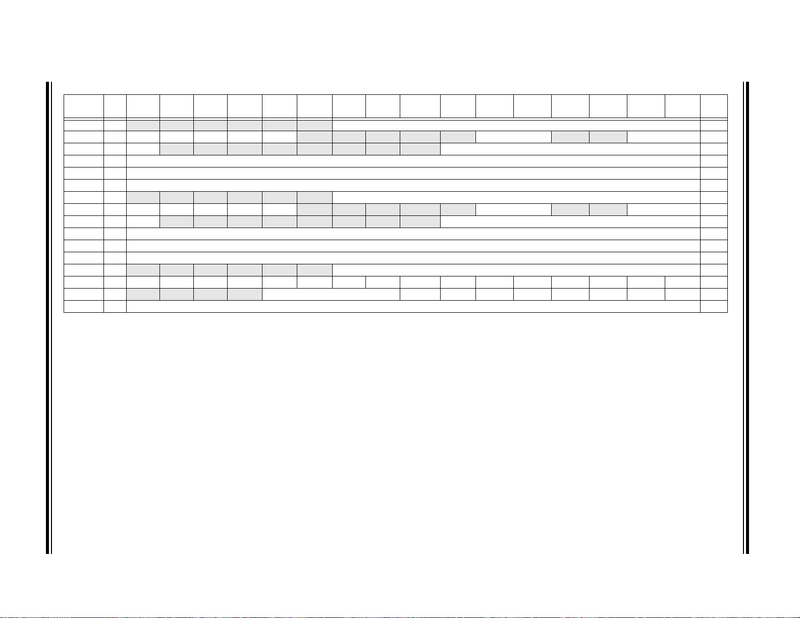
© 2009 Microchip Technology Inc. DS70286C-page 51
TABLE 4-17: DMA REGISTER MAP (CONTINUED)
File Name Addr Bit 15 Bit 14 Bit 13 Bit 12 Bit 11 Bit 10 Bit 9 Bit 8 Bit 7 Bit 6 Bit 5 Bit 4 Bit 3 Bit 2 Bit 1 Bit 0
DMA5CNT 03C6 — — — — — — CNT<9:0> 0000
DMA6CON 03C8 CHEN SIZE DIR HALF NULLW
DMA6REQ 03CA FORCE
DMA6STA 03CC STA<15:0> 0000
DMA6STB 03CE STB<15:0> 0000
DMA6PAD 03D0 PAD<15:0> 0000
DMA6CNT 03D2
DMA7CON 03D4 CHEN SIZE DIR HALF NULLW
DMA7REQ 03D6 FORCE
DMA7STA 03D8 STA<15:0> 0000
DMA7STB 03DA STB<15:0> 0000
DMA7PAD 03DC PAD<15:0> 0000
DMA7CNT 03DE
DMACS0 03E0 PWCOL7 PWCOL6 PWCOL5 PWCOL4 PWCOL3 PWCOL2 PWCOL1 PWCOL0 XWCOL7 XWCOL6 XWCOL5 XWCOL4 XWCOL3 XWCOL2 XWCOL1 XWCOL0 0000
DMACS1 03E2
DSADR 03E4 DSADR<15:0> 0000
Legend: — = unimplemented, read as ‘0’. Reset values are shown in hexadecimal.
— — — — — — CNT<9:0> 0000
— — — — — — CNT<9:0> 0000
— — — — LSTCH<3:0> PPST7 PPST6 PPST5 PPST4 PPST3 PPST2 PPST1 PPST0 0000
— — — — — — — — IRQSEL<6:0> 0000
— — — — — — — — IRQSEL<6:0> 0000
— — — — —AMODE<1:0> — —MODE<1:0>0000
— — — — —AMODE<1:0> — —MODE<1:0>0000
All
Resets
dsPIC33FJXXXGPX06/X08/X10
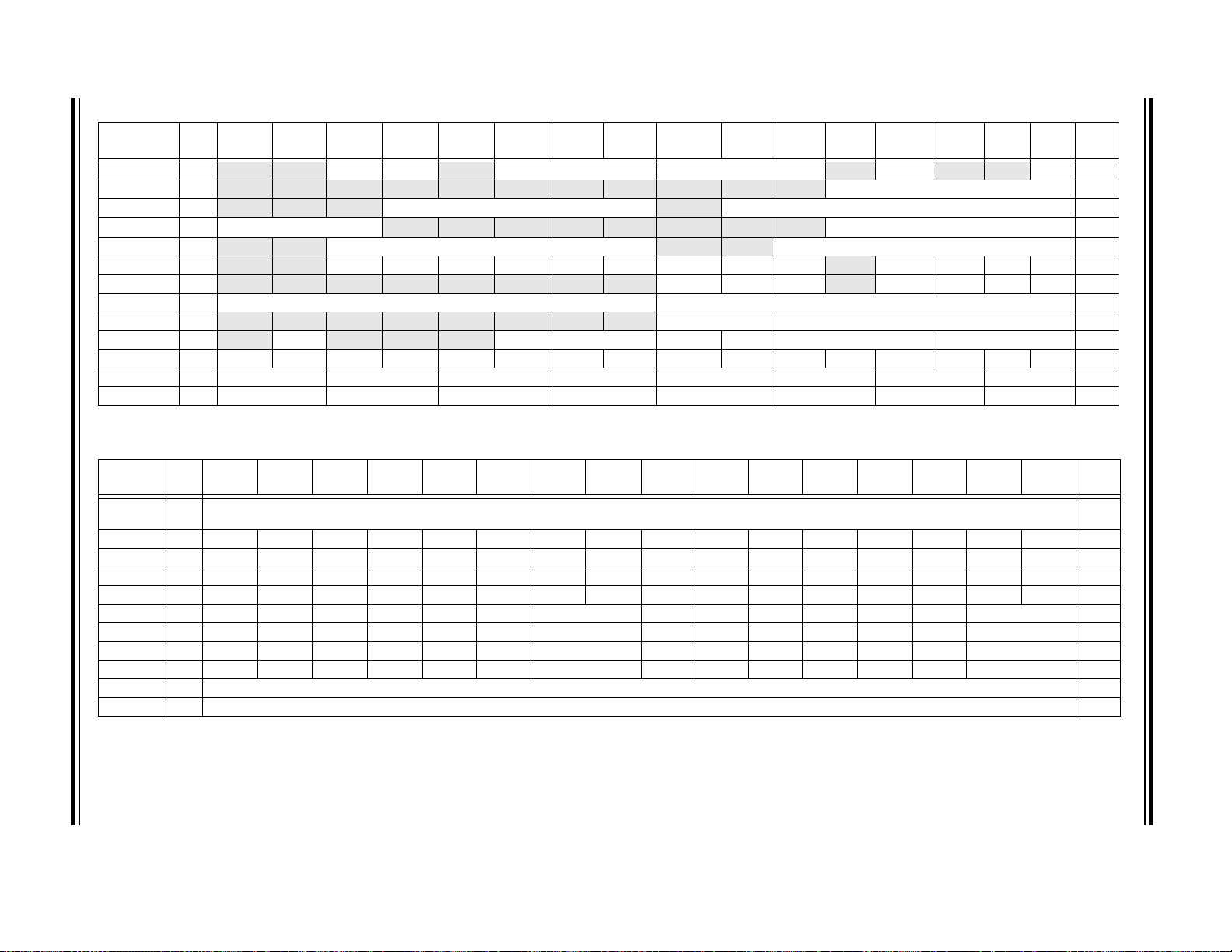
DS70286C-page 52 © 2009 Microchip Technology Inc.
TABLE 4-18: ECAN1 REGISTER MAP WHEN C1CTRL1.WIN = 0 OR 1 FOR dsPIC33FJXXXGP506/510/706/708/710 DEVICES ONLY
File Name Addr Bit 15 Bit 14 Bit 13 Bit 12 Bit 11 Bit 10 Bit 9 Bit 8 Bit 7 Bit 6 Bit 5 Bit 4 Bit 3 Bit 2 Bit 1 Bit 0
C1CTRL1 0400
C1CTRL2 0402
C1VEC 0404
C1FCTRL 0406 DMABS<2:0>
C1FIFO 0408
C1INTF 040A
C1INTE 040C
C1EC 040E TERRCNT<7:0> RERRCNT<7:0> 0000
C1CFG1 0410
C1CFG2 0412
C1FEN1 0414
C1FMSKSEL1 0418 F7MSK<1:0> F6MSK<1:0> F5MSK<1:0> F4MSK<1:0> F3MSK<1:0> F2MSK<1:0> F1MSK<1:0> F0MSK<1:0> 0000
C1FMSKSEL2 041A F15MSK<1:0> F14MSK<1:0> F13MSK<1:0> F12MSK<1:0> F11MSK<1:0> F10MSK<1:0> F9MSK<1:0> F8MSK<1:0> 0000
Legend: — = unimplemented, read as ‘0’. Reset values are shown in hexadecimal.
— — CSIDL ABAT — REQOP<2:0> OPMODE<2:0> —CANCAP — —WIN0480
— — — — — — — — — — — DNCNT<4:0> 0000
— — — FILHIT<4:0> — ICODE<6:0> 0000
— — — — — — — —
— —FBP<5:0> — — FNRB<5:0> 0000
— — TXBO TXBP RXBP TXWAR RXWAR EWARN IVRIF WAKIF ERRIF — FIFOIF RBOVIF RBIF TBIF 0000
— — — — — — — — IVRIE WAKIE ERRIE — FIFOIE RBOVIE RBIE TBIE 0000
— — — — — — — — SJW<1:0> BRP<5:0> 0000
—WAKFIL— — — SEG2PH<2:0> SEG2PHTS SAM SEG1PH<2:0> PRSEG<2:0> 0000
FLTEN15 FLTEN14 FLTEN13 FLTEN12 FLTEN11 FLTEN10 FLTEN9 FLTEN8 FLTEN7 FLTEN6 FLTEN5 FLTEN4 FLTEN3 FLTEN2 FLTEN1 FLTEN0
FSA<4:0>
All
Resets
0000
FFFF
TABLE 4-19: ECAN1 REGISTER MAP WHEN C1CTRL1.WIN = 0 FOR dsPIC33FJXXXGP506/510/706/708/710 DEVICES ONLY
File Name Addr Bit 15 Bit 14 Bit 13 Bit 12 Bit 11 Bit 10 Bit 9 Bit 8 Bit 7 Bit 6 Bit 5 Bit 4 Bit 3 Bit 2 Bit 1 Bit 0
0400-
041E
C1RXFUL1 0420 RXFUL15 RXFUL14 RXFUL13 RXFUL12 RXFUL11 RXFUL10 RXFUL9 RXFUL8 RXFUL7 RXFUL6 RXFUL5 RXFUL4 RXFUL3 RXFUL2 RXFUL1 RXFUL0 0000
C1RXFUL2 0422 RXFUL31 RXFUL30 RXFUL29 RXFUL28 RXFUL27 RXFUL26 RXFUL25 RXFUL24 RXFUL23 RXFUL22 RXFUL21 RXFUL20 RXFUL19 RXFUL18 RXFUL17 RXFUL16 0000
C1RXO VF1 0428 RXOVF15 RXOVF14 RXOVF13 RXOVF12 RXOVF11 RXOVF10 RXOVF9 RXOVF8 RXOVF7 RXOVF6 RXOVF5 RXOVF4 RXOVF3 RXOVF2 RXOVF1 RXOVF0 0000
C1RXOVF2 042A RXOVF31 RXOVF30 RXOVF29 RXOVF28 RXOVF27 RXOVF26 RXOVF25 RXOVF24 RXOVF23 RXOVF22 RXOVF21 RXOVF20 RXOVF19 RXOVF18 RXOVF17 RXOVF16 0000
C1TR01CON 0430
C1TR23CON 0432
C1TR45CON 0434
C1TR67CON 0436
C1RXD 0440 Received Data Word xxxx
C1TXD 0442 Transmit Data Word xxxx
Legend: x = unknown value on Reset, — = unimplemented, read as ‘0’. Reset values are shown in hexadecimal.
TXEN1 TXABT1 TXLARB1 TXERR1 TXREQ1 RTREN1 TX1PRI<1:0> TXEN0 TXABAT0 TXLARB0 TXERR0 TXREQ0 RTREN0 TX0PRI<1:0>
TXEN3 TXABT3 TXLARB3 TXERR3 TXREQ3 RTREN3 TX3PRI<1:0> TXEN2 TXABAT2 TXLARB2 TXERR2 TXREQ2 RTREN2 TX2PRI<1:0>
TXEN5 TXABT5 TXLARB5 TXERR5 TXREQ5 RTREN5 TX5PRI<1:0> TXEN4 TXABAT4 TXLARB4 TXERR4 TXREQ4 RTREN4 TX4PRI<1:0>
TXEN7 TXABT7 TXLARB7 TXERR7 TXREQ7 RTREN7 TX7PRI<1:0> TXEN6 TXABAT6 TXLARB6 TXERR6 TXREQ6 RTREN6 TX6PRI<1:0>
See definition when WIN = x
All
Resets
0000
0000
0000
xxxx
dsPIC33FJXXXGPX06/X08/X10

© 2009 Microchip Technology Inc. DS70286C-page 53
TABLE 4-20: ECAN1 REGISTER MAP WHEN C1CTRL1.WIN = 1 FOR dsPIC33FJXXXGP506/510/706/708/710 DEVICES ONLY
File Name Addr Bit 15 Bit 14 Bit 13 Bit 12 Bit 11 Bit 10 Bit 9 Bit 8 Bit 7 Bit 6 Bit 5 Bit 4 Bit 3 Bit 2 Bit 1 Bit 0
0400-
041E
C1BUFPNT1 0420 F3BP<3:0> F2BP<3:0> F1BP<3:0> F0BP<3:0> 0000
C1BUFPNT2 0422 F7BP<3:0> F6BP<3:0> F5BP<3:0> F4BP<3:0> 0000
C1BUFPNT3 0424 F11BP<3:0> F10BP<3:0> F9BP<3:0> F8BP<3:0> 0000
C1BUFPNT4 0426 F15BP<3:0> F14BP<3:0> F13BP<3:0> F12BP<3:0> 0000
C1RXM0SID 0430 SID<10:3> SID<2:0>
C1RXM0EID 0432 EID<15:8> EID<7:0> xxxx
C1RXM1SID 0434 SID<10:3> SID<2:0>
C1RXM1EID 0436 EID<15:8> EID<7:0> xxxx
C1RXM2SID 0438 SID<10:3> SID<2:0>
C1RXM2EID 043A EID<15:8> EID<7:0> xxxx
C1RXF0SID 0440 SID<10:3> SID<2:0>
C1RXF0EID 0442 EID<15:8> EID<7:0> xxxx
C1RXF1SID 0444 SID<10:3> SID<2:0>
C1RXF1EID 0446 EID<15:8> EID<7:0> xxxx
C1RXF2SID 0448 SID<10:3> SID<2:0>
C1RXF2EID 044A EID<15:8> EID<7:0> xxxx
C1RXF3SID 044C SID<10:3> SID<2:0>
C1RXF3EID 044E EID<15:8> EID<7:0> xxxx
C1RXF4SID 0450 SID<10:3> SID<2:0>
C1RXF4EID 0452 EID<15:8> EID<7:0> xxxx
C1RXF5SID 0454 SID<10:3> SID<2:0>
C1RXF5EID 0456 EID<15:8> EID<7:0> xxxx
C1RXF6SID 0458 SID<10:3> SID<2:0>
C1RXF6EID 045A EID<15:8> EID<7:0> xxxx
C1RXF7SID 045C SID<10:3> SID<2:0>
C1RXF7EID 045E EID<15:8> EID<7:0> xxxx
C1RXF8SID 0460 SID<10:3> SID<2:0>
C1RXF8EID 0462 EID<15:8> EID<7:0> xxxx
C1RXF9SID 0464 SID<10:3> SID<2:0>
C1RXF9EID 0466 EID<15:8> EID<7:0> xxxx
C1RXF10SID 0468 SID<10:3> SID<2:0>
C1RXF10EID 046A EID<15:8> EID<7:0> xxxx
Legend: x = unknown value on Reset, — = unimplemented, read as ‘0’. Reset values are shown in hexadecimal.
See definition when WIN = x
—MIDE— EID<17:16> xxxx
—MIDE— EID<17:16> xxxx
—MIDE— EID<17:16> xxxx
—EXIDE— EID<17:16> xxxx
—EXIDE— EID<17:16> xxxx
—EXIDE— EID<17:16> xxxx
—EXIDE— EID<17:16> xxxx
—EXIDE— EID<17:16> xxxx
—EXIDE— EID<17:16> xxxx
—EXIDE— EID<17:16> xxxx
—EXIDE— EID<17:16> xxxx
—EXIDE— EID<17:16> xxxx
—EXIDE— EID<17:16> xxxx
—EXIDE— EID<17:16> xxxx
All
Resets
dsPIC33FJXXXGPX06/X08/X10
DS70286C-page 54 © 2009 Microchip Technology Inc.
TABLE 4-20: ECAN1 REGISTER MAP WHEN C1CTRL1.WIN = 1 FOR dsPIC33FJXXXGP506/510/706/708/710 DEVICES ONLY (CONTINUED)
File Name Addr Bit 15 Bit 14 Bit 13 Bit 12 Bit 11 Bit 10 Bit 9 Bit 8 Bit 7 Bit 6 Bit 5 Bit 4 Bit 3 Bit 2 Bit 1 Bit 0
C1RXF11SID 046C SID<10:3> SID<2:0> —EXIDE— EID<17:16> xxxx
C1RXF11EID 046E EID<15:8> EID<7:0> xxxx
C1RXF12SID 0470 SID<10:3> SID<2:0>
C1RXF12EID 0472 EID<15:8> EID<7:0> xxxx
C1RXF13SID 0474 SID<10:3> SID<2:0>
C1RXF13EID 0476 EID<15:8> EID<7:0> xxxx
C1RXF14SID 0478 SID<10:3> SID<2:0>
C1RXF14EID 047A EID<15:8> EID<7:0> xxxx
C1RXF15SID 047C SID<10:3> SID<2:0>
C1RXF15EID 047E EID<15:8> EID<7:0> xxxx
Legend: x = unknown value on Reset, — = unimplemented, read as ‘0’. Reset values are shown in hexadecimal.
—EXIDE— EID<17:16> xxxx
—EXIDE— EID<17:16> xxxx
—EXIDE— EID<17:16> xxxx
—EXIDE— EID<17:16> xxxx
All
Resets
dsPIC33FJXXXGPX06/X08/X10
© 2009 Microchip Technology Inc. DS70286C-page 55
TABLE 4-21: ECAN2 REGISTER MAP WHEN C2CTRL1.WIN = 0 OR 1 FOR dsPIC33FJXXXGP706/708/710 DEVICES ONLY
File Name Addr Bit 15 Bit 14 Bit 13 Bit 12 Bit 11 Bit 10 Bit 9 Bit 8 Bit 7 Bit 6 Bit 5 Bit 4 Bit 3 Bit 2 Bit 1 Bit 0
C2CTRL1 0500
C2CTRL2 0502
C2VEC 0504
C2FCTRL 0506 DMABS<2:0>
C2FIFO 0508
C2INTF 050A
C2INTE 050C
C2EC 050E TERRCNT<7:0> RERRCNT<7:0> 0000
C2CFG1 0510
C2CFG2 0512
C2 FEN1 05 14 F LTE N15 FLT EN1 4 FLTEN 13 FLTEN 12 F LTEN 11 F LTEN 10 F LTEN 9 FLTE N8 F LTEN7 F LTE N6 FLTE N5 FLT EN 4 FLTEN 3 F LTEN 2 FLT EN1 F LTE N0 FFFF
C2FMSKSEL1 0518 F7MSK<1:0> F6MSK<1:0> F5MSK<1:0> F4MSK<1:0> F3MSK<1:0> F2MSK<1:0> F1MSK<1:0> F0MSK<1:0> 0000
C2FMSKSEL2 051A F15MSK<1:0> F14MSK<1:0> F13MSK<1:0> F12MSK<1:0> F11MSK<1:0> F10MSK<1:0> F9MSK<1:0> F8MSK<1:0> 0000
Legend: — = unimplemented, read as ‘0’. Reset values are shown in hexadecimal.
— —CSIDLABAT — REQOP<2:0> OPMODE<2:0> — CANCAP — —WIN0480
— — — — — — — — — — — DNCNT<4:0> 0000
— — — FILHIT<4:0> — ICODE<6:0> 0000
— — — — — — — —
— — FBP<5:0> — — FNRB<5:0> 0000
— — TXBO TXBP RXBP TXWAR RXWAR EWARN IVRIF WAKIF ERRIF — FIFOIF RBOVIF RBIF TBIF 0000
— — — — — — — — IVRIE WAKIE ERRIE — FIFOIE RBOVIE RBIE TBIE 0000
— — — — — — — — SJW<1:0> BRP<5:0> 0000
— WAKFIL — — — SEG2PH<2:0> SEG2PHTS SAM SEG1PH<2:0> PRSEG<2:0> 0000
FSA<4:0>
All
Resets
0000
TABLE 4-22: ECAN2 REGISTER MAP WHEN C2CTRL1.WIN = 0 FOR dsPIC33FJXXXGP706/708/710 DEVICES ONLY
File Name Addr Bit 15 Bit 14 Bit 13 Bit 12 Bit 11 Bit 10 Bit 9 Bit 8 Bit 7 Bit 6 Bit 5 Bit 4 Bit 3 Bit 2 Bit 1 Bit 0
0500-
051E
C2RXFUL1 0520 RXFUL15 RXFUL14 RXFUL13 RXFUL12 RXFUL11 RXFUL10 RXFUL9 RXFUL8 RXFUL7 RXFUL6 RXFUL5 RXFUL4 RXFUL3 RXFUL2 RXFUL1 RXFUL0 0000
C2RXFUL2 0522 RXFUL31 RXFUL30 RXFUL29 RXFUL28 RXFUL27 RXFUL26 RXFUL25 RXFUL24 RXFUL23 RXFUL22 RXFUL21 RXFUL20 RXFUL19 RXFUL18 RXFUL17 RXFUL16 0000
C2RXO VF1 0528 RXOVF15 RXOVF14 RXOVF13 RXOVF12 RXOVF11 RXOVF10 RXOVF09 RXOVF08 RXOVF7 RXOVF6 RXOVF5 RXOVF4 RXOVF3 RXOVF2 RXOVF1 RXOVF0 0000
C2RXOVF2 052A RXOVF31 RXOVF30 RXOVF29 RXOVF28 RXOVF27 RXOVF26 RXOVF25 RXOVF24 RXOVF23 RXOVF22 RXOVF21 RXOVF20 RXOVF19 RXOVF18 RXOVF17 RXOVF16 0000
C2TR01CON 0530 TXEN1 TX
C2TR23CON 0532 TXEN3 TX
C2TR45CON 0534 TXEN5 TX
C2TR67CON 0536 TXEN7 TX
C2RXD 0540 Recieved Data Word xxxx
C2TXD 0542 Transmit Data Word xxxx
Legend: x = unknown value on Reset, — = unimplemented, read as ‘0’. Reset values are shown in hexadecimal.
ABAT1TXLARB1TXERR1TXREQ1
ABAT3TXLARB3TXERR3TXREQ3
ABAT5TXLARB5TXERR5TXREQ5
ABAT7TXLARB7TXERR7TXREQ7
RTREN1 TX1PRI<1:0> TXEN0 TX
RTREN3 TX3PRI<1:0> TXEN2 TX
RTREN5 TX5PRI<1:0> TXEN4 TX
RTREN7 TX7PRI<1:0> TXEN6 TX
See definition when WIN = x
ABAT0TXLARB0TXERR0TXREQ0
ABAT2TXLARB2TXERR2TXREQ2
ABAT4TXLARB4TXERR4TXREQ4
ABAT6TXLARB6TXERR6TXREQ6
RTREN0 TX0PRI<1:0> 0000
RTREN2 TX2PRI<1:0> 0000
RTREN4 TX4PRI<1:0> 0000
RTREN6 TX6PRI<1:0> xxxx
All
Resets
dsPIC33FJXXXGPX06/X08/X10

DS70286C-page 56 © 2009 Microchip Technology Inc.
TABLE 4-23: ECAN2 REGISTER MAP WHEN C2CTRL1.WIN = 1 FOR dsPIC33FJXXXGP706/708/710 DEVICES ONLY
File Name Addr Bit 15 Bit 14 Bit 13 Bit 12 Bit 11 Bit 10 Bit 9 Bit 8 Bit 7 Bit 6 Bit 5 Bit 4 Bit 3 Bit 2 Bit 1 Bit 0
0500
-
051E
C2BUFPNT1 0520 F3BP<3:0> F2BP<3:0> F1BP<3:0> F0BP<3:0> 0000
C2BUFPNT2 0522 F7BP<3:0> F6BP<3:0> F5BP<3:0> F4BP<3:0> 0000
C2BUFPNT3 0524 F11BP<3:0> F10BP<3:0> F9BP<3:0> F8BP<3:0> 0000
C2BUFPNT4 0526 F15BP<3:0> F14BP<3:0> F13BP<3:0> F12BP<3:0> 0000
C2RXM0SID 0530 SID<10:3> SID<2:0>
C2RXM0EID 0532 EID<15:8> EID<7:0> xxxx
C2RXM1SID 0534 SID<10:3> SID<2:0>
C2RXM1EID 0536 EID<15:8> EID<7:0> xxxx
C2RXM2SID 0538 SID<10:3> SID<2:0>
C2RXM2EID 053A EID<15:8> EID<7:0> xxxx
C2RXF0SID 0540 SID<10:3> SID<2:0>
C2RXF0EID 0542 EID<15:8> EID<7:0> xxxx
C2RXF1SID 0544 SID<10:3> SID<2:0>
C2RXF1EID 0546 EID<15:8> EID<7:0> xxxx
C2RXF2SID 0548 SID<10:3> SID<2:0>
C2RXF2EID 054A EID<15:8> EID<7:0> xxxx
C2RXF3SID 054C SID<10:3> SID<2:0>
C2RXF3EID 054E EID<15:8> EID<7:0> xxxx
C2RXF4SID 0550 SID<10:3> SID<2:0>
C2RXF4EID 0552 EID<15:8> EID<7:0> xxxx
C2RXF5SID 0554 SID<10:3> SID<2:0>
C2RXF5EID 0556 EID<15:8> EID<7:0> xxxx
C2RXF6SID 0558 SID<10:3> SID<2:0>
C2RXF6EID 055A EID<15:8> EID<7:0> xxxx
C2RXF7SID 055C SID<10:3> SID<2:0>
C2RXF7EID 055E EID<15:8> EID<7:0> xxxx
C2RXF8SID 0560 SID<10:3> SID<2:0>
C2RXF8EID 0562 EID<15:8> EID<7:0> xxxx
C2RXF9SID 0564 SID<10:3> SID<2:0>
C2RXF9EID 0566 EID<15:8> EID<7:0> xxxx
C2RXF10SID 0568 SID<10:3> SID<2:0>
Legend: x = unknown value on Reset, — = unimplemented, read as ‘0’. Reset values are shown in hexadecimal.
See definition when WIN = x
—MIDE— EID<17:16> xxxx
—MIDE— EID<17:16> xxxx
—MIDE— EID<17:16> xxxx
— EXIDE — EID<17:16> xxxx
— EXIDE — EID<17:16> xxxx
— EXIDE — EID<17:16> xxxx
— EXIDE — EID<17:16> xxxx
— EXIDE — EID<17:16> xxxx
— EXIDE — EID<17:16> xxxx
— EXIDE — EID<17:16> xxxx
— EXIDE — EID<17:16> xxxx
— EXIDE — EID<17:16> xxxx
— EXIDE — EID<17:16> xxxx
— EXIDE — EID<17:16> xxxx
Resets
dsPIC33FJXXXGPX06/X08/X10
All

© 2009 Microchip Technology Inc. DS70286C-page 57
TABLE 4-23: ECAN2 REGISTER MAP WHEN C2CTRL1.WIN = 1 FOR dsPIC33FJXXXGP706/708/710 DEVICES ONLY (CONTINUED)
File Name Addr Bit 15 Bit 14 Bit 13 Bit 12 Bit 11 Bit 10 Bit 9 Bit 8 Bit 7 Bit 6 Bit 5 Bit 4 Bit 3 Bit 2 Bit 1 Bit 0
C2RXF10EID 056A EID<15:8> EID<7:0> xxxx
C2RXF11SID 056C SID<10:3> SID<2:0>
C2RXF11EID 056E EID<15:8> EID<7:0> xxxx
C2RXF12SID 0570 SID<10:3> SID<2:0>
C2RXF12EID 0572 EID<15:8> EID<7:0> xxxx
C2RXF13SID 0574 SID<10:3>
C2RXF13EID 0576 EID<15:8>
C2RXF14SID 0578 SID<10:3>
C2RXF14EID 057A EID<15:8>
C2RXF15SID 057C SID<10:3>
C2RXF15EID 057E EID<15:8> EID<7:0> xxxx
Legend: x = unknown value on Reset, — = unimplemented, read as ‘0’. Reset values are shown in hexadecimal.
SID<2:0>
SID<2:0>
SID<2:0>
— EXIDE — EID<17:16> xxxx
— EXIDE — EID<17:16> xxxx
— EXIDE — EID<17:16>
EID<7:0>
— EXIDE — EID<17:16>
EID<7:0>
— EXIDE — EID<17:16>
Resets
xxxx
xxxx
xxxx
xxxx
xxxx
All
dsPIC33FJXXXGPX06/X08/X10

DS70286C-page 58 © 2009 Microchip Technology Inc.
TABLE 4-24: DCI REGISTER MAP
SFR
Name
DCICON1 0280 DCIEN
DCICON2 0282
DCICON3 0284
DCISTAT 0286
TSCON 0288 TSE15 TSE14 TSE13 TSE12 TSE11 TSE10 TSE9 TSE8 TSE7 TSE6 TSE5 TSE4 TSE3 TSE2 TSE1 TSE0 0000 0000 0000 0000
RSCON 028C RSE15 RSE14 RSE13 RSE12 RSE11 RSE10 RSE9 RSE8 RSE7 RSE6 RSE5 RSE4 RSE3 RSE2 RSE1 RSE0 0000 0000 0000 0000
RXBUF0 0290 Receive Buffer #0 Data Register 0000 0000 0000 0000
RXBUF1 0292 Receive Buffer #1 Data Register 0000 0000 0000 0000
RXBUF2 0294 Receive Buffer #2 Data Register 0000 0000 0000 0000
RXBUF3 0296 Receive Buffer #3 Data Register 0000 0000 0000 0000
TXBUF0 0298 Transmit Buffer #0 Data Register 0000 0000 0000 0000
TXBUF1 029A Transmit Buffer #1 Data Register 0000 0000 0000 0000
TXBUF2 029C Transmit Buffer #2 Data Register 0000 0000 0000 0000
TXBUF3 029E Transmit Buffer #3 Data Register 0000 0000 0000 0000
Legend: — = unimplemented, read as ‘0’.
Note 1: Refer to the “dsPIC33F Family Reference Manual” for descriptions of register bit fields.
TABLE 4-25: PORTA REGISTER MAP
File Name Addr Bit 15 Bit 14 Bit 13 Bit 12 Bit 11 Bit 10 Bit 9 Bit 8 Bit 7 Bit 6 Bit 5 Bit 4 Bit 3 Bit 2 Bit 1 Bit 0
TRISA 02C0
PORTA 02C2
LATA 02C4
ODCA
Legend: x = unknown value on Reset, — = unimplemented, read as ‘0’. Reset values are shown in hexadecimal for PinHigh devices.
Note 1: The actual set of I/O port pins varies from one device to another. Please refer to the corresponding pinout diagrams.
Addr. Bit 15 Bit 14 Bit 13 Bit 12 Bit 11 Bit 10 Bit 9 Bit 8 Bit 7 Bit 6 Bit 5 Bit 4 Bit 3 Bit 2 Bit 1 Bit 0 Reset State
—DCISIDL— DLOOP CSCKD CSCKE COFSD UNFM CSDOM DJST — — — COFSM1 COFSM0 0000 0000 0000 0000
— — — —BLEN1BLEN0 —COFSG<3:0>—WS<3:0>0000 0000 0000 0000
— — — — BCG<11:0> 0000 0000 0000 0000
— — — — SLOT3 SLOT2 SLOT1 SLOT0 — — — — ROV RFUL TUNF TMPTY 0000 0000 0000 0000
(1)
TRISA15 TRISA14 TRISA13 TRISA12 — TRISA10 TRISA9 — TRISA7 TRISA6 TRISA5 TRISA4 TRISA3 TRISA2 TRISA1 TRISA0
RA15 RA14 RA13 RA12 — RA10 RA9 — RA7 RA6 RA5 RA4 RA3 RA2 RA1 RA0
(2)
LATA15 LATA14 LATA13 LATA12 — LATA10 LATA9 — LATA7 LATA6 LATA5 LATA4 LATA3 LATA2 LATA1 LATA0
06C0
ODCA15 ODCA14
— — — — — — — —
ODCA5 ODCA4 ODCA3 ODCA2 ODCA1 ODCA0
All
Resets
F6FF
xxxx
xxxx
0000
dsPIC33FJXXXGPX06/X08/X10
TABLE 4-26: PORTB REGISTER MAP
File Name Addr Bit 15 Bit 14 Bit 13 Bit 12 Bit 11 Bit 10 Bit 9 Bit 8 Bit 7 Bit 6 Bit 5 Bit 4 Bit 3 Bit 2 Bit 1 Bit 0
TRISB 02C6 TRISB15 TRISB14 TRISB13 TRISB12 TRISB11 TRISB10 TRISB9 TRISB8 TRISB7 TRISB6 TRISB5 TRISB4 TRISB3 TRISB2 TRISB1 TRISB0
PORTB 02C8 RB15 RB14 RB13 RB12 RB11 RB10 RB9 RB8 RB7 RB6 RB5 RB4 RB3 RB2 RB1 RB0
LAT B 02 CA L ATB 15 L ATB1 4 LAT B1 3 LAT B12 LAT B11 L ATB 10 L ATB 9 L ATB 8 LAT B7 L ATB6 L ATB5 L ATB 4 LAT B3 L ATB2 LAT B1 L ATB 0
Legend: x = unknown value on Reset, — = unimplemented, read as ‘0’. Reset values are shown in hexadecimal for PinHigh devices.
Note 1: The actual set of I/O port pins varies from one device to another. Please refer to the corresponding pinout diagrams.
(1)
All
Resets
FFFF
xxxx
xxxx

© 2009 Microchip Technology Inc. DS70286C-page 59
TABLE 4-27: PORTC REGISTER MAP
File Name Addr Bit 15 Bit 14 Bit 13 Bit 12 Bit 11 Bit 10 Bit 9 Bit 8 Bit 7 Bit 6 Bit 5 Bit 4 Bit 3 Bit 2 Bit 1 Bit 0
TRISC 02CC TRISC15 TRISC14 TRISC13 TRISC12 — — — — — — —
PORTC 02CE RC15 RC14 RC13 RC12 — — — — — — —
LATC 02D0 LATC15 LATC14 LATC13 LATC12 — — — — — — —
Legend: x = unknown value on Reset, — = unimplemented, read as ‘0’. Reset values are shown in hexadecimal for PinHigh devices.
Note 1: The actual set of I/O port pins varies from one device to another. Please refer to the corresponding pinout diagrams.
(1)
TRISC4 TRISC3 TRISC2 TRISC1 —
RC4 RC3 RC2 RC1 —
LATC4 LATC3 LATC2 LATC1 —
All
Resets
F01E
xxxx
xxxx
TABLE 4-28: PORTD REGISTER MAP
File Name Addr Bit 15 Bit 14 Bit 13 Bit 12 Bit 11 Bit 10 Bit 9 Bit 8 Bit 7 Bit 6 Bit 5 Bit 4 Bit 3 Bit 2 Bit 1 Bit 0
TRISD 02D2
PORTD 02D4
LATD 02D6
ODCD 06D2
Legend: x = unknown value on Reset, — = unimplemented, read as ‘0’. Reset values are shown in hexadecimal for PinHigh devices.
Note 1: The actual set of I/O port pins varies from one device to another. Please refer to the corresponding pinout diagrams.
TRISD15 TRISD14 TRISD13 TRISD12
RD15 RD14 RD13 RD12
LATD15 LATD14 LATD13 LATD12
ODCD15 ODCD14 ODCD13 ODCD12 ODCD11 ODCD10 ODCD9 ODCD8 ODCD7 ODCD6 ODCD5 ODCD4 ODCD3 ODCD2 ODCD1 ODCD0
TABLE 4-29: PORTE REGISTER MAP
File Name Addr Bit 15 Bit 14 Bit 13 Bit 12 Bit 11 Bit 10 Bit 9 Bit 8 Bit 7 Bit 6 Bit 5 Bit 4 Bit 3 Bit 2 Bit 1 Bit 0
TRISE 02D8 — — — — — — — —
PORTE 02DA — — — — — — — —
LATE 02DC — — — — — — — —
Legend: x = unknown value on Reset, — = unimplemented, read as ‘0’. Reset values are shown in hexadecimal for PinHigh devices.
Note 1: The actual set of I/O port pins varies from one device to another. Please refer to the corresponding pinout diagrams.
TABLE 4-30: PORTF REGISTER MAP
File Name Addr Bit 15 Bit 14 Bit 13 Bit 12 Bit 11 Bit 10 Bit 9 Bit 8 Bit 7 Bit 6 Bit 5 Bit 4 Bit 3 Bit 2 Bit 1 Bit 0 All Resets
TRISF 02DE — —
PORTF 02E0 — —
LATF 02E2 — —
ODCF 06DE — —
Legend: x = unknown value on Reset, — = unimplemented, read as ‘0’. Reset values are shown in hexadecimal for PinHigh devices.
Note 1: The actual set of I/O port pins varies from one device to another. Please refer to the corresponding pinout diagrams.
TRISF13 TRISF12
RF13 RF12
LATF13 LATF12
ODCF13 ODCF12
(1)
(1)
(1)
TRISD11 TRISD10 TRISD9 TRISD8 TRISD7 TRISD6 TRISD5 TRISD4 TRISD3 TRISD2 TRISD1 TRISD0
RD11 RD10 RD9 RD8 RD7 RD6 RD5 RD4 RD3 RD2 RD1 RD0
LATD11 LATD10 LATD9 LATD8 LATD7 LATD6 LATD5 LATD4 LATD3 LATD2 LATD1 LATD0
TRISE7
LATE7
— — —
— — — RF8 RF7 RF6 RF5 RF4 RF3 RF2 RF1 RF0
— — — LATF8 LATF7 LATF6 LATF5 LATF4 LATF3 LATF2 LATF1 LATF0
— — —
TRISF8 TRISF7
ODCF8 ODCF7 ODCF6 ODCF5 ODCF4 ODCF3 ODCF2 ODCF1 ODCF0
TRISE6 TRISE5 TRISE4 TRISE3 TRISE2 TRISE1 TRISE0
RE7
RE6 RE5 RE4 RE3 RE2 RE1 RE0
LATE6 LATE5 LATE4 LATE3 LATE2 LATE1 LATE0
TRISF6 TRISF5 TRISF4 TRISF3 TRISF2 TRISF1 TRISF0
All
Resets
FFFF
xxxx
xxxx
0000
All
Resets
00FF
xxxx
xxxx
31FF
xxxx
xxxx
0000
dsPIC33FJXXXGPX06/X08/X10

DS70286C-page 60 © 2009 Microchip Technology Inc.
TABLE 4-31: PORTG REGISTER MAP
File Name Addr Bit 15 Bit 14 Bit 13 Bit 12 Bit 11 Bit 10 Bit 9 Bit 8 Bit 7 Bit 6 Bit 5 Bit 4 Bit 3 Bit 2 Bit 1 Bit 0
TRISG 02E4
PORTG 02E6
LATG 02E8
ODCG 06E4
Legend: x = unknown value on Reset, — = unimplemented, read as ‘0’. Reset values are shown in hexadecimal for PinHigh devices.
Note 1: The actual set of I/O port pins varies from one device to another. Please refer to the corresponding pinout diagrams.
TRISG15 TRISG14 TRISG13 TRISG12 — — TRISG9 TRISG8 TRISG7 TRISG6 — — TRISG3 TRISG2 TRISG1 TRISG0
RG15 RG14 RG13 RG12 — — RG9 RG8 RG7 RG6 — — RG3 RG2 RG1 RG0
LATG15 LATG14 LATG13 LATG12 — — L ATG 9 LAT G8 LAT G7 LAT G6 — — LATG3 LATG2 LATG1 LATG0
ODCG15 ODCG14 ODCG13 ODCG12
(1)
— —
ODCG9 ODCG8 ODCG7 ODCG6
— —
ODCG3 ODCG2 ODCG1 ODCG0
All
Resets
F3CF
xxxx
xxxx
0000
TABLE 4-32: SYSTEM CONTROL REGISTER MAP
File Name Addr Bit 15 Bit 14 Bit 13 Bit 12 Bit 11 Bit 10 Bit 9 Bit 8 Bit 7 Bit 6 Bit 5 Bit 4 Bit 3 Bit 2 Bit 1 Bit 0
RCON 0740 TRAPR IOPUWR — — — — — VREGS EXTR SWR SWDTEN WDTO SLEEP IDLE BOR POR
OSCCON 0742 — COSC<2:0> — NOSC<2:0> CLKLOCK —LOCK—CF— LPOSCEN OSWEN 0300
CLKDIV 0744 ROI DOZE<2:0> DOZEN FRCDIV<2:0> PLLPOST<1:0> — PLLPRE<4:0> 3040
PLLFBD 0746
OSCTUN 0748
Legend: x = unknown value on Reset, — = unimplemented, read as ‘0’. Reset values are shown in hexadecimal.
Note 1: RCON register Reset values dependent on type of Reset.
2: OSCCON register Reset values dependent on the FOSC Configuration bits and by type of Reset.
— — — — — — — PLLDIV<8:0> 0030
— — — — — — — — — —TUN<5:0>0000
Resets
xxxx
TABLE 4-33: NVM REGISTER MAP
File Name Addr Bit 15 Bit 14 Bit 13 Bit 12 Bit 11Bit 10Bit 9Bit 8Bit 7Bit 6Bit 5Bit 4Bit 3Bit 2Bit 1Bit 0
NVMCON 0760 WR WREN WRERR — — — — — —ERASE— —NVMOP<3:0>
NVMKEY 0766
Legend: x = unknown value on Reset, — = unimplemented, read as ‘0’. Reset values are shown in hexadecimal.
Note 1: Reset value shown is for POR only. Value on other Reset states is dependent on the state of memory write or erase operations at the time of Reset.
— — — — — — — — NVMKEY<7:0>
Resets
0000
0000
dsPIC33FJXXXGPX06/X08/X10
All
(1)
(2)
All
(1)
TABLE 4-34: PMD REGISTER MAP
File Name Addr Bit 15 Bit 14 Bit 13 Bit 12 Bit 11 Bit 10 Bit 9 Bit 8 Bit 7 Bit 6 Bit 5 Bit 4 Bit 3 Bit 2 Bit 1 Bit 0
PMD1 0770 T5MD T4MD T3MD T2MD T1MD
PMD2 0772 IC8MD IC7MD IC6MD IC5MD IC4MD IC3MD IC2MD IC1MD OC8MD OC7MD OC6MD OC5MD OC4MD OC3MD OC2MD OC1MD 0000
PMD3 0774 T9MD T8MD T7MD T6MD
Legend: x = unknown value on Reset, — = unimplemented, read as ‘0’. Reset values are shown in hexadecimal.
— — — — — — — — — —I2C2MDAD2MD0000
— —
DCIMD I2C1MD U2MD U1MD SPI2MD SPI1MD C2MD C1MD AD1MD 0000
All
Resets

dsPIC33FJXXXGPX06/X08/X10
<Free Word>
PC<15:0>
000000000
015
W15 (before CALL)
W15 (after CALL)
Stack Grows Towards
Higher Address
0x0000
PC<22:16>
POP : [--W15]
PUSH : [W15++]
4.2.7 SOFTWARE STACK
In addition to its use as a working register, the W15
register in the dsPIC33FJXXXGPX06/X08/X10 devices
is also used as a software Stack Pointer. The Stack
Pointer always points to the first available free word
and grows from lower to higher addresses. It
pre-decrements for stack pops and post-increments for
stack pushes, as shown in Figure 4-6. For a PC push
during any CALL instruction, the MSb of the PC is
zero-extended before the push, ensuring that the MSb
is always clear.
Note: A PC push during exception processing
concatenates the SRL register to the MSb
of the PC prior to the push.
The Stack Pointer Limit register (SPLIM) associated
with the Stack Pointer sets an upper address boundary
for the stack. SPLIM is uninitialized at Reset. As is the
case for the Stack Pointer, SPLIM<0> is forced to ‘0’
because all stack operations must be word-aligned.
Whenever an EA is generated using W15 as a source
or destination pointer, the resulting address is
compared with the value in SPLIM. If the contents of
the Stack Pointer (W15) and the SPLIM register are
equal and a push operation is performed, a stack error
trap will not occur. The stack error trap will occur on a
subsequent push operation. Thus, for example, if it is
desirable to cause a stack error trap when the stack
grows beyond address 0x2000 in RAM, initialize the
SPLIM with the value 0x1FFE.
Similarly, a Stack Pointer underflow (stack error) trap is
generated when the Stack Pointer address is found to
be less than 0x0800. This prevents the stack from
interfering with the Special Function Register (SFR)
space.
A write to the SPLIM register should not be immediately
followed by an indirect read operation using W15.
FIGURE 4-6: CALL STACK FRAME
4.2.8 DATA RAM PROTECTION FEATURE
The dsPIC33F product family supports Data RAM
protection features which enable segments of RAM to
be protected when used in conjunction with Boot and
Secure Code Segment Security. BSRAM (Secure RAM
segment for BS) is accessible only from the Boot
Segment Flash code when enabled. SSRAM (Secure
RAM segment for RAM) is accessible only from the
Secure Segment Flash code when enabled. See
Table 4-1 for an overview of the BSRAM and SSRAM
SFRs.
4.3 Instruction Addressing Modes
The addressing modes in Table 4-35 form the basis of
the addressing modes optimized to support the specific
features of individual instructions. The addressing
modes provided in the MAC class of instructions are
somewhat different from those in the other instruction
types.
4.3.1 FILE REGISTER INSTRUCTIONS
Most file register instructions use a 13-bit address field
(f) to directly address data present in the first 8192
bytes of data memory (Near Data Space). Most file
register instructions employ a working register, W0,
which is denoted as WREG in these instructions. The
destination is typically either the same file register or
WREG (with the exception of the MUL instruction),
which writes the result to a register or register pair. The
MOV instruction allows additional flexibility and can
access the entire data space.
4.3.2 MCU INSTRUCTIONS
The 3-operand MCU instructions are of the form:
Operand 3 = Operand 1 <function> Operand 2
where Operand 1 is always a working register (i.e., the
addressing mode can only be register direct) which is
referred to as Wb. Operand 2 can be a W register,
fetched from data memory, or a 5-bit literal. The result
location can be either a W register or a data memory
location. The following addressing modes are
supported by MCU instructions:
• Register Direct
• Register Indirect
• Register Indirect Post-Modified
• Register Indirect Pre-Modified
• 5-bit or 10-bit Literal
Note: Not all instructions support all the
addressing modes given above. Individual
instructions may support different subsets
of these addressing modes.
© 2009 Microchip Technology Inc. DS70286C-page 61

dsPIC33FJXXXGPX06/X08/X10
TABLE 4-35: FUNDAMENTAL ADDRESSING MODES SUPPORTED
Addressing Mode Description
File Register Direct The address of the file register is specified explicitly.
Register Direct The contents of a register are accessed directly.
Register Indirect The contents of Wn forms the EA.
Register Indirect Post-Modified The contents of Wn forms the EA. Wn is post-modified (incremented or
decremented) by a constant value.
Register Indirect Pre-Modified Wn is pre-modified (incremented or decremented) by a signed constant value
to form the EA.
Register Indirect with Register Offset The sum of Wn and Wb forms the EA.
Register Indirect with Literal Offset The sum of Wn and a literal forms the EA.
4.3.3 MOVE AND ACCUMULATOR INSTRUCTIONS
Move instructions and the DSP accumulator class of
instructions provide a greater degree of addressing
flexibility than other instructions. In addition to the
Addressing modes supported by most MCU
instructions, move and accumulator instructions also
support Register Indirect with Register Offset
Addressing mode, also referred to as Register Indexed
mode.
Note: For the MOV instructions, the Addressing
mode specified in the instruction can differ
for the source and destination EA.
However, the 4-bit Wb (Register Offset)
field is shared between both source and
destination (but typically only used by
one).
In summary, the following Addressing modes are
supported by move and accumulator instructions:
• Register Direct
• Register Indirect
• Register Indirect Post-modified
• Register Indirect Pre-modified
• Register Indirect with Register Offset (Indexed)
• Register Indirect with Literal Offset
• 8-bit Literal
• 16-bit Literal
Note: Not all instructions support all the
Addressing modes given above. Individual
instructions may support different subsets
of these Addressing modes.
4.3.4 MAC INSTRUCTIONS
The dual source operand DSP instructions (CLR, ED,
EDAC, MAC, MPY, MPY.N, MOVSAC and MSC), also referred
to as MAC instructions, utilize a simplified set of
addressing modes to allow the user to effectively
manipulate the data pointers through register indirect
tables.
The 2-source operand prefetch registers must be
members of the set {W8, W9, W10, W11}. For data
reads, W8 and W9 are always directed to the X RAGU
and W10 and W11 will always be directed to the Y
AGU. The effective addresses generated (before and
after modification) must, therefore, be valid addresses
within X data space for W8 and W9 and Y data space
for W10 and W11.
Note: Register Indirect with Register Offset
Addressing mode is only available for W9
(in X space) and W11 (in Y space).
In summary, the following addressing modes are
supported by the MAC class of instructions:
• Register Indirect
• Register Indirect Post-Modified by 2
• Register Indirect Post-Modified by 4
• Register Indirect Post-Modified by 6
• Register Indirect with Register Offset (Indexed)
4.3.5 OTHER INSTRUCTIONS
Besides the various addressing modes outlined above,
some instructions use literal constants of various sizes.
For example, BRA (branch) instructions use 16-bit signed
literals to specify the branch destination directly, whereas
the DISI instruction uses a 14-bit unsigned literal field. In
some instructions, such as ADD Acc, the source of an
operand or result is implied by the opcode itself. Certain
operations, such as NOP, do not have any operands.
4.4 Modulo Addressing
Modulo Addressing mode is a method of providing an
automated means to support circular data buffers using
hardware. The objective is to remove the need for
software to perform data address boundary checks
when executing tightly looped code, as is typical in
many DSP algorithms.
Modulo Addressing can operate in either data or program
space (since the data pointer mechanism is essentially
the same for both). One circular buffer can be supported
in each of the X (which also provides the pointers into
program space) and Y data spaces. Modulo Addressing
DS70286C-page 62 © 2009 Microchip Technology Inc.
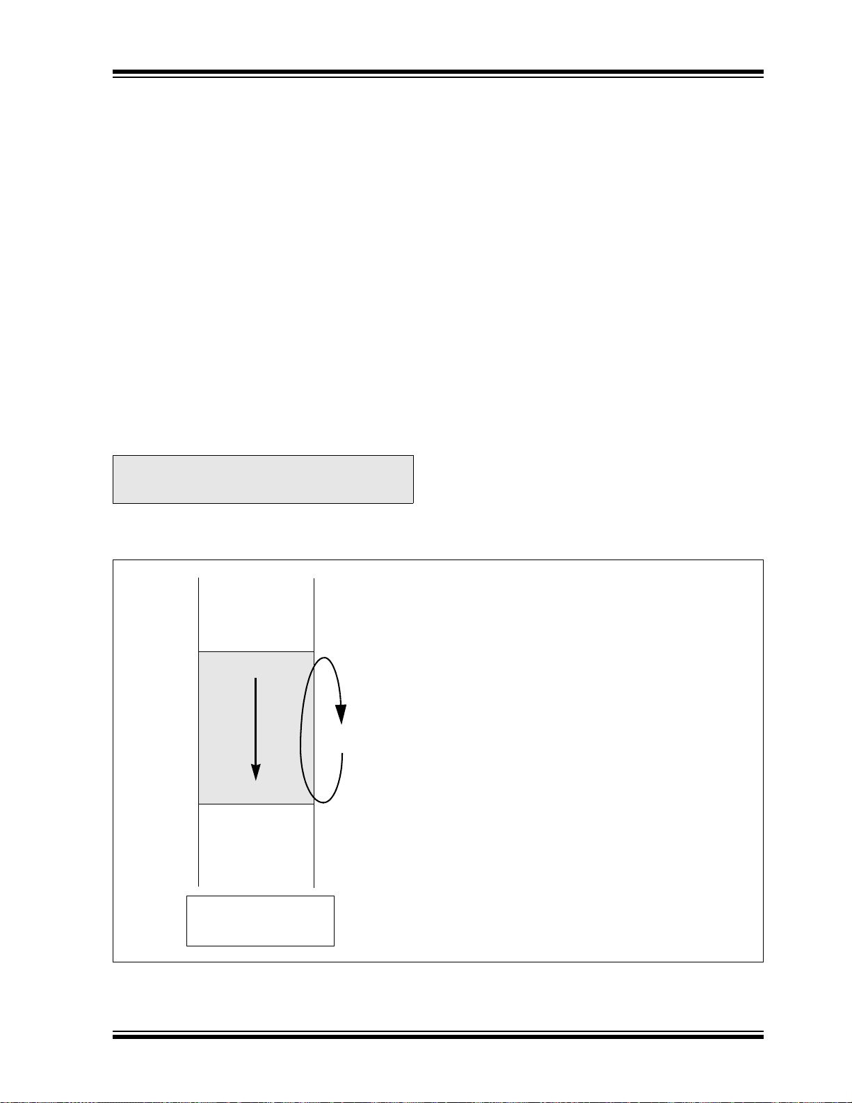
dsPIC33FJXXXGPX06/X08/X10
0x1100
0x1163
Start Addr = 0x1100
End Addr = 0x1163
Length = 0x0032 words
Byte
Address
MOV #0x1100, W0
MOV W0, XMODSRT ;set modulo start address
MOV #0x1163, W0
MOV W0, MODEND ;set modulo end address
MOV #0x8001, W0
MOV W0, MODCON ;enable W1, X AGU for modulo
MOV #0x0000, W0 ;W0 holds buffer fill value
MOV #0x1110, W1 ;point W1 to buffer
DO AGAIN, #0x31 ;fill the 50 buffer locations
MOV W0, [W1++] ;fill the next location
AGAIN: INC W0, W0 ;increment the fill value
can operate on any W register pointer. However, it is not
advisable to use W14 or W15 for Modulo Addressing
since these two registers are used as the Stack Frame
Pointer and Stack Pointer, respectively.
In general, any particular circular buffer can only be
configured to operate in one direction as there are
certain restrictions on the buffer start address (for incrementing buffers), or end address (for decrementing
buffers), based upon the direction of the buffer.
The only exception to the usage restrictions is for
buffers which have a power-of-2 length. As these
buffers satisfy the start and end address criteria, they
may operate in a bidirectional mode (i.e., address
boundary checks will be performed on both the lower
and upper address boundaries).
4.4.1 START AND END ADDRESS
The Modulo Addressing scheme requires that a starting
and ending address be specified and loaded into the
16-bit Modulo Buffer Address registers: XMODSRT,
XMODEND, YMODSRT and YMODEND (see
Table 4-1).
Note: Y space Modulo Addressing EA
calculations assume word sized data (LSb
of every EA is always clear).
The length of a circular buffer is not directly specified. It
is determined by the difference between the
corresponding start and end addresses. The maximum
possible length of the circular buffer is 32K words
(64 Kbytes).
4.4.2 W ADDRESS REGISTER SELECTION
The Modulo and Bit-Reversed Addressing Control
register, MODCON<15:0>, contains enable flags as well
as a W register field to specify the W Address registers.
The XWM and YWM fields select which registers will
operate with Modulo Addressing. If XWM = 15, X RAGU
and X WAGU Modulo Addressing is disabled. Similarly, if
YWM = 15, Y AGU Modulo Addressing is disabled.
The X Address Space Pointer W register (XWM), to
which Modulo Addressing is to be applied, is stored in
MODCON<3:0> (see Table 4-1). Modulo Addressing is
enabled for X data space when XWM is set to any value
other than ‘15’ and the XMODEN bit is set at
MODCON<15>.
The Y Address Space Pointer W register (YWM) to
which Modulo Addressing is to be applied is stored in
MODCON<7:4>. Modulo Addressing is enabled for Y
data space when YWM is set to any value other than
‘15’ and the YMODEN bit is set at MODCON<14>.
FIGURE 4-7: MODULO ADDRESSING OPERATION EXAMPLE
© 2009 Microchip Technology Inc. DS70286C-page 63

dsPIC33FJXXXGPX06/X08/X10
4.4.3 MODULO ADDRESSING APPLICABILITY
Modulo Addressing can be applied to the Effective
Address (EA) calculation associated with any W
register. It is important to realize that the address
boundaries check for addresses less than, or greater
than, the upper (for incrementing buffers) and lower (for
decrementing buffers) boundary addresses (not just
equal to). Address changes may, therefore, jump
beyond boundaries and still be adjusted correctly.
Note: The modulo corrected effective address is
written back to the register only when
Pre-Modify or Post-Modify Addressing
mode is used to compute the effective
address. When an address offset (e.g.,
[W7+W2]) is used, Modulo Address
correction is performed but the contents of
the register remain unchanged.
4.5 Bit-Reversed Addressing
Bit-Reversed Addressing mode is intended to simplify
data re-ordering for radix-2 FFT algorithms. It is
supported by the X AGU for data writes only.
The modifier, which may be a constant value or register
contents, is regarded as having its bit order reversed. The
address source and destination are kept in normal order.
Thus, the only operand requiring reversal is the modifier.
4.5.1 BIT-REVERSED ADDRESSING IMPLEMENTATION
Bit-Reversed Addressing mode is enabled when:
1. BWM bits (W register selection) in the
MODCON register are any value other than ‘15’
(the stack cannot be accessed using
Bit-Reversed Addressing).
2. The BREN bit is set in the XBREV register.
3. The addressing mode used is Register Indirect
with Pre-Increment or Post-Increment.
If the length of a bit-reversed buffer is M = 2
the last ‘N’ bits of the data buffer start address must
be zeros.
XB<14:0> is the Bit-Reversed Address modifier, or
‘pivot point’, which is typically a constant. In the case of
an FFT computation, its value is equal to half of the FFT
data buffer size.
Note: All bit-reversed EA calculations assume
word sized data (LSb of every EA is
always clear). The XB value is scaled
accordingly to generate compatible (byte)
addresses.
When enabled, Bit-Reversed Addressing is only
executed for Register Indirect with Pre-Increment or
Post-Increment Addressing and word sized data writes.
It will not function for any other addressing mode or for
byte sized data and normal addresses are generated
instead. When Bit-Reversed Addressing is active, the
W Address Pointer is always added to the address
modifier (XB) and the offset associated with the Register Indirect Addressing mode is ignored. In addition, as
word sized data is a requirement, the LSb of the EA is
ignored (and always clear).
Note: Modulo Addressing and Bit-Reversed
Addressing should not be enabled
together. In the event that the user attempts
to do so, Bit-Reversed Addressing will
assume priority when active for the X
WAGU and X WAGU Modulo Addressing
will be disabled. However, Modulo
Addressing will continue to function in the X
RAGU.
If Bit-Reversed Addressing has already been enabled
by setting the BREN (XBREV<15>) bit, then a write to
the XBREV register should not be immediately followed
by an indirect read operation using the W register that
has been designated as the bit-reversed pointer.
N
bytes,
DS70286C-page 64 © 2009 Microchip Technology Inc.

dsPIC33FJXXXGPX06/X08/X10
b3 b2 b1 0
b2 b3 b4 0
Bit Locations Swapped Left-to-Right
Around Center of Binary Value
Bit-Reversed Address
XB = 0x0008 for a 16-Word Bit-Reversed Buffer
b7 b6 b5 b1
b7 b6 b5 b4b11 b10 b9 b8
b11 b10 b9 b8
b15 b14 b13 b12
b15 b14 b13 b12
Sequential Address
Pivot Point
FIGURE 4-8: BIT-REVERSED ADDRESS EXAMPLE
TABLE 4-36: BIT-REVERSED ADDRESS SEQUENCE (16-ENTRY)
Normal Address Bit-Reversed Address
A3A2A1A0 Decimal A3A2A1A0 Decimal
0000 0 0000 0
0001 1 1000 8
0010 2 0100 4
0011 3 1100 12
0100 4 0010 2
0101 5 1010 10
0110 6 0110 6
0111 7 1110 14
1000 8 0001 1
1001 9 1001 9
1010 10 0101 5
1011 11 1101 13
1100 12 0011 3
1101 13 1011 11
1110 14 0111 7
1111 15 1111 15
© 2009 Microchip Technology Inc. DS70286C-page 65

dsPIC33FJXXXGPX06/X08/X10
4.6 Interfacing Program and Data
Memory Spaces
The dsPIC33FJXXXGPX06/X08/X10 architecture uses
a 24-bit wide program space and a 16-bit wide data
space. The architecture is also a modified Harvard
scheme, meaning that data can also be present in the
program space. To use this data successfully, it must
be accessed in a way that preserves the alignment of
information in both spaces.
Aside from normal execution, the
dsPIC33FJXXXGPX06/X08/X10 architecture provides
two methods by which program space can be accessed
during operation:
• Using table instructions to access individual bytes
or words anywhere in the program space
• Remapping a portion of the program space into
the data space (Program Space Visibility)
Table instructions allow an application to read or write
to small areas of the program memory. This capability
makes the method ideal for accessing data tables that
need to be updated from time to time. It also allows
access to all bytes of the program word. The
remapping method allows an application to access a
large block of data on a read-only basis, which is ideal
for look ups from a large table of static data. It can only
access the least significant word of the program word.
4.6.1 ADDRESSING PROGRAM SPACE
Since the address ranges for the data and program
spaces are 16 and 24 bits, respectively, a method is
needed to create a 23-bit or 24-bit program address
from 16-bit data registers. The solution depends on the
interface method to be used.
For table operations, the 8-bit Table Page register
(TBLPAG) is used to define a 32K word region within
the program space. This is concatenated with a 16-bit
EA to arrive at a full 24-bit program space address. In
this format, the Most Significant bit of TBLPAG is used
to determine if the operation occurs in the user memory
(TBLPAG<7> = 0) or the configuration memory
(TBLPAG<7> = 1).
For remapping operations, the 8-bit Program Space
Visibility register (PSVPAG) is used to define a
16K word page in the program space. When the Most
Significant bit of the EA is ‘1’, PSVPAG is concatenated
with the lower 15 bits of the EA to form a 23-bit program
space address. Unlike table operations, this limits
remapping operations strictly to the user memory area.
Table 4-37 and Figure 4-9 show how the program EA is
created for table operations and remapping accesses
from the data EA. Here, P<23:0> refers to a program
space word, whereas D<15:0> refers to a data space
word.
TABLE 4-37: PROGRAM SPACE ADDRESS CONSTRUCTION
Access Type
Instruction Access
(Code Execution)
TBLRD/TBLWT
(Byte/Word Read/Write)
Program Space Visibility
(Block Remap/Read)
Note 1: Data EA<15> is always ‘1’ in this case, but is not used in calculating the program space address. Bit 15 of
the address is PSVPAG<0>.
Access
Space
User 0 PC<22:1> 0
User TBLPAG<7:0> Data EA<15:0>
Configuration TBLPAG<7:0> Data EA<15:0>
User 0 PSVPAG<7:0> Data EA<14:0>
<23> <22:16> <15> <14:1> <0>
0xx xxxx xxxx xxxx xxxx xxx0
0xxx xxxx xxxx xxxx xxxx xxxx
1xxx xxxx xxxx xxxx xxxx xxxx
0 xxxx xxxx xxx xxxx xxxx xxxx
Program Space Address
(1)
DS70286C-page 66 © 2009 Microchip Technology Inc.

dsPIC33FJXXXGPX06/X08/X10
0Program Counter
23 bits
1
PSVPAG
8 bits
EA
15 bits
Program Counter
(1)
Select
TBLPAG
8 bits
EA
16 bits
Byte Select
0
0
1/0
User/Configuration
Table Operations
(2)
Program Space Visibility
(1)
Space Select
24 bits
23 bits
(Remapping)
1/0
0
Note 1: The LSb of program space addresses is always fixed as ‘0’ in order to maintain word
alignment of data in the program and data spaces.
2: Table operations are not required to be word-aligned. Table read operations are permitted
in the configuration memory space.
FIGURE 4-9: DATA ACCESS FROM PROGRAM SPACE ADDRESS GENERATION
© 2009 Microchip Technology Inc. DS70286C-page 67

dsPIC33FJXXXGPX06/X08/X10
081623
00000000
00000000
00000000
00000000
‘Phantom’ Byte
TBLRDH.B (Wn<0> = 0)
TBLRDL.W
TBLRDL.B (Wn<0> = 1)
TBLRDL.B (Wn<0> = 0)
23 15 0
TBLPAG
02
0x000000
0x800000
0x020000
0x030000
Program Space
The address for the table operation is determined by the data EA
within the page defined by the TBLPAG register.
Only read operations are shown; write operations are also valid in
the user memory area.
4.6.2 DATA ACCESS FROM PROGRAM MEMORY USING TABLE INSTRUCTIONS
The TBLRDL and TBLWTL instructions offer a direct
method of reading or writing the lower word of any
address within the program space without going
through data space. The TBLRDH and TBLWTH
instructions are the only method to read or write the
upper 8 bits of a program space word as data.
The PC is incremented by two for each successive
24-bit program word. This allows program memory
addresses to directly map to data space addresses.
Program memory can thus be regarded as two 16-bit
word wide address spaces, residing side by side, each
with the same address range. TBLRDL and TBLWTL
access the space which contains the least significant
data word and TBLRDH and TBLWTH access the space
which contains the upper data byte.
Two table instructions are provided to move byte or
word sized (16-bit) data to and from program space.
Both function as either byte or word operations.
1. TBLRDL (Table Read Low): In Word mode, it
maps the lower word of the program space
location (P<15:0>) to a data address (D<15:0>).
In Byte mode, either the upper or lower byte of
the lower program word is mapped to the lower
byte of a data address. The upper byte is
selected when Byte Select is ‘1’; the lower byte
is selected when it is ‘0’.
2. TBLRDH (Table Read High): In Word mode, it
maps the entire upper word of a program address
(P<23:16>) to a data address. Note that
D<15:8>, the ‘phantom byte’, will always be ‘0’.
In Byte mode, it maps the upper or lower byte of
the program word to D<7:0> of the data
address, as above. Note that the data will
always be ‘0’ when the upper ‘phantom’ byte is
selected (Byte Select = 1).
In a similar fashion, two table instructions, TBLWTH
and TBLWTL, are used to write individual bytes or
words to a program space address. The details of
their operation are explained in Section 5.0 “Flash
Program Memory”.
For all table operations, the area of program memory
space to be accessed is determined by the Table Page
register (TBLPAG). TBLPAG covers the entire program
memory space of the device, including user and
configuration spaces. When TBLPAG<7> = 0, the table
page is located in the user memory space. When
TBLPAG<7> = 1, the page is located in configuration
space.
FIGURE 4-10: ACCESSING PROGRAM MEMORY WITH TABLE INSTRUCTIONS
DS70286C-page 68 © 2009 Microchip Technology Inc.
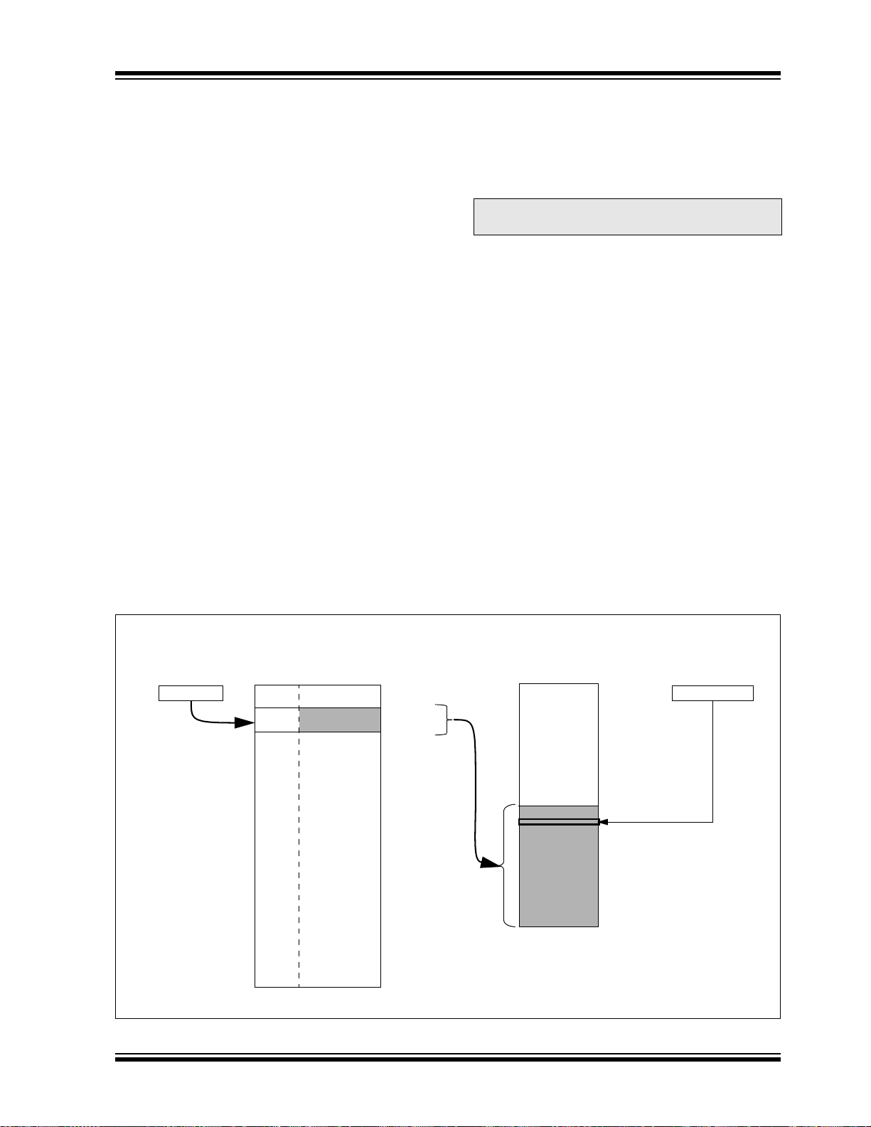
dsPIC33FJXXXGPX06/X08/X10
23 15 0
PSVPAG
Data Space
Program Space
0x0000
0x8000
0xFFFF
02
0x000000
0x800000
0x010000
0x018000
When CORCON<2> = 1 and EA<15> = 1:
The data in the page
designated by PSVPAG is mapped into
the upper half of the
data memory
space...
Data EA<14:0>
...while the lower 15 bits
of the EA specify an
exact address within
the PSV area. This
corresponds exactly to
the same lower 15 bits
of the actual program
space address.
PSV Area
4.6.3 READING DATA FROM PROGRAM MEMORY USING PROGRAM SPACE VISIBILITY
The upper 32 Kbytes of data space may optionally be
mapped into any 16K word page of the program space.
This option provides transparent access of stored
constant data from the data space without the need to
use special instructions (i.e., TBLRDL/H).
Program space access through the data space occurs
if the Most Significant bit of the data space EA is ‘1’ and
program space visibility is enabled by setting the PSV
bit in the Core Control register (CORCON<2>). The
location of the program memory space to be mapped
into the data space is determined by the Program
Space Visibility Page register (PSVPAG). This 8-bit
register defines any one of 256 possible pages of
16K words in program space. In effect, PSVPAG
functions as the upper 8 bits of the program memory
address, with the 15 bits of the EA functioning as the
lower bits. Note that by incrementing the PC by 2 for
each program memory word, the lower 15 bits of data
space addresses directly map to the lower 15 bits in the
corresponding program space addresses.
Data reads to this area add an additional cycle to the
instruction being executed, since two program memory
fetches are required.
Although each data space address, 8000h and higher,
maps directly into a corresponding program memory
address (see Figure 4-11), only the lower 16 bits of the
24-bit program word are used to contain the data. The
upper 8 bits of any program space location used as
data should be programmed with ‘1111 1111’ or
‘0000 0000’ to force a NOP. This prevents possible
issues should the area of code ever be accidentally
executed.
Note: PSV access is temporarily disabled during
table reads/writes.
For operations that use PSV and are executed outside
a REPEAT loop, the MOV and MOV.D instructions
require one instruction cycle in addition to the specified
execution time. All other instructions require two
instruction cycles in addition to the specified execution
time.
For operations that use PSV, which are executed inside
a REPEAT loop, there will be some instances that
require two instruction cycles in addition to the
specified execution time of the instruction:
• Execution in the first iteration
• Execution in the last iteration
• Execution prior to exiting the loop due to an
interrupt
• Execution upon re-entering the loop after an
interrupt is serviced
Any other iteration of the REPEAT loop will allow the
instruction accessing data, using PSV, to execute in a
single cycle.
FIGURE 4-11: PROGRAM SPACE VISIBILITY OPERATION
© 2009 Microchip Technology Inc. DS70286C-page 69

dsPIC33FJXXXGPX06/X08/X10
NOTES:
DS70286C-page 70 © 2009 Microchip Technology Inc.
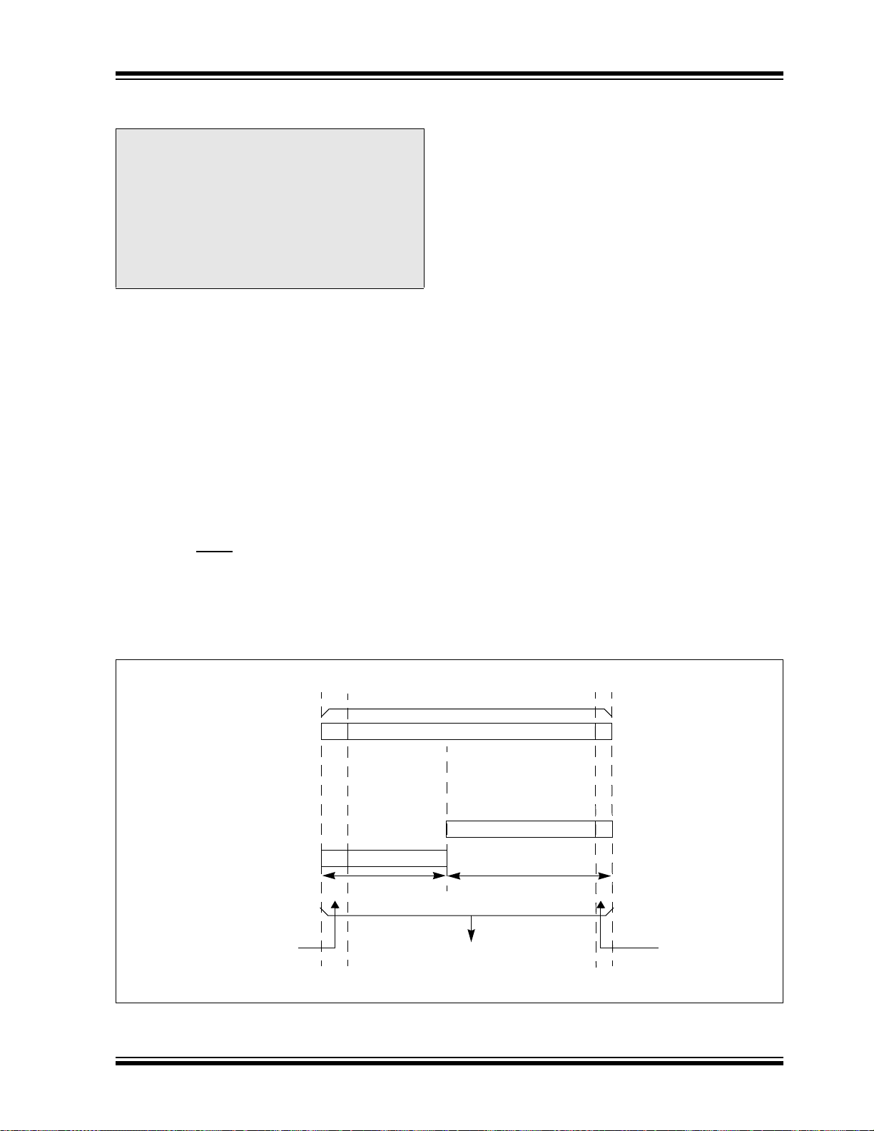
dsPIC33FJXXXGPX06/X08/X10
0
Program Counter
24 bits
Program Counter
TBLPAG Reg
8 bits
Working Reg EA
16 bits
Byte
24-bit EA
0
1/0
Select
Using
Table Instruction
Using
User/Configuration
Space Select
5.0 FLASH PROGRAM MEMORY
Note: This data sheet summarizes the features
of the dsPIC33FJXXXGPX06/X08/X10
family of devices. However, it is not
intended to be a comprehensive reference
source. To complement the information in
this data sheet, refer to Section 5. “Flash
Programming” (DS70191) in the
“dsPIC33F Family Reference Manual”,
which is available from the Microchip web
site (www.microchip.com).
The dsPIC33FJXXXGPX06/X08/X10 devices contain
internal Flash program memory for storing and
executing application code. The memory is readable,
writable and erasable during normal operation over the
entire V
Flash memory can be programmed in two ways:
1. In-Circuit Serial Programming™ (ICSP™)
2. Run-Time Self-Programming (RTSP)
ICSP allows a dsPIC33FJXXXGPX06/X08/X10 device
to be serially programmed while in the end application
circuit. This is simply done with two lines for
programming clock and programming data (one of the
alternate programming pin pairs: PGECx/PGEDx), and
three other lines for power (V
Master Clear (MCLR). This allows customers to manufacture boards with unprogrammed devices and then
DD range.
programming capability
DD), ground (VSS) and
program the digital signal controller just before shipping
the product. This also allows the most recent firmware
or a custom firmware to be programmed.
RTSP is accomplished using TBLRD (table read) and
TBLWT (table write) instructions. With RTSP, the user
can write program memory data either in blocks or
‘rows’ of 64 instructions (192 bytes) at a time or a single
program memory word, and erase program memory in
blocks or ‘pages’ of 512 instructions (1536 bytes) at a
time.
5.1 Table Instructions and Flash
Programming
Regardless of the method used, all programming of
Flash memory is done with the table read and table
write instructions. These allow direct read and write
access to the program memory space from the data
memory while the device is in normal operating mode.
The 24-bit target address in the program memory is
formed using bits<7:0> of the TBLPAG register and the
Effective Address (EA) from a W register specified in
the table instruction, as shown in Figure 5-1.
The TBLRDL and the TBLWTL instructions are used to
read or write to bits<15:0> of program memory.
TBLRDL and TBLWTL can access program memory in
both Word and Byte modes.
The TBLRDH and TBLWTH instructions are used to read
or write to bits<23:16> of program memory. TBLRDH
and TBLWTH can also access program memory in Word
or Byte mode.
FIGURE 5-1: ADDRESSING FOR TABLE REGISTERS
© 2009 Microchip Technology Inc. DS70286C-page 71

dsPIC33FJXXXGPX06/X08/X10
T
7.37 MHz FRC Accuracy()% FRC Tuning()%××
--------------------------------------------------------------------------------------------------------------------------
T
RW
11064 Cycles
7.37 MHz 10.02+()1 0.00375–()××
----------------------------------------------------------------------------------------------
1.48ms==
T
RW
11064 Cycles
7.37 MHz 10.02–()1 0.00375–()××
----------------------------------------------------------------------------------------------
1.54ms==
5.2 RTSP Operation
The dsPIC33FJXXXGPX06/X08/X10 Flash program
memory array is organized into rows of 64 instructions
or 192 bytes. RTSP allows the user to erase a page of
memory, which consists of eight rows (512 instructions)
at a time, and to program one row or one word at a
time. Table 25-12 illustrates typical erase and programming times. The 8-row erase pages and single row
write rows are edge-aligned, from the beginning of program memory, on boundaries of 1536 bytes and 192
bytes, respectively.
The program memory implements holding buffers that
can contain 64 instructions of programming data. Prior
to the actual programming operation, the write data
must be loaded into the buffers in sequential order. The
instruction words loaded must always be from a group
of 64 boundary.
The basic sequence for RTSP programming is to set up
a Table Pointer, then do a series of TBLWT instructions
to load the buffers. Programming is performed by
setting the control bits in the NVMCON register. A total
of 64 TBLWTL and TBLWTH instructions are required
to load the instructions.
All of the table write operations are single-word writes
(two instruction cycles) because only the buffers are
written. A programming cycle is required for
programming each row.
5.3 Programming Operations
A complete programming sequence is necessary for
programming or erasing the internal Flash in RTSP
mode. The processor stalls (waits) until the
programming operation is finished.
The programming time depends on the FRC accuracy
(see Table 25-19) and the value of the FRC Oscillator
Tuning register (see Register 9-4). Use the following
formula to calculate the minimum and maximum values
for the Row Write Time, Page Erase Time and Word
Write Cycle Time parameters (see Table 25-12).
EQUATION 5-1: PROGRAMMING TIME
For example, if the device is operating at +85°C, the
FRC accuracy will be ±2%. If the TUN<5:0> bits (see
Register 9-4) are set to ‘b111111, the Minimum
Row Write Time is:
and, the Maximum Row Write Time is:
Setting the WR bit (NVMCON<15>) starts the operation, and the WR bit is automatically cleared when the
operation is finished.
5.4 Control Registers
There are two SFRs used to read and write the
program Flash memory:
• NVMCON: Flash Memory Control Register
• NVMKEY: Non-Volatile Memory Key Register
The NVMCON register (Register 5-1) controls which
blocks are to be erased, which memory type is to be
programmed and the start of the programming cycle.
NVMKEY (Register 5-2) is a write-only register that is
used for write protection. To start a programming or
erase sequence, the user must consecutively write 55h
and AAh to the NVMKEY register. Refer to Section 5.3
“Programming Operations” for further details.
DS70286C-page 72 © 2009 Microchip Technology Inc.

dsPIC33FJXXXGPX06/X08/X10
REGISTER 5-1: NVMCON: FLASH MEMORY CONTROL REGISTER
(1)
R/SO-0
WR WREN WRERR
bit 15 bit 8
R/W-0
(1)
R/W-0
(1)
U-0 U-0 U-0 U-0 U-0
— — — — —
U-0 R/W-0
(1)
U-0 U-0 R/W-0
— ERASE — —NVMOP<3:0>
(1)
R/W-0
(1)
R/W-0
(2)
(1)
R/W-0
(1)
bit 7 bit 0
Legend: SO = Settable only bit
R = Readable bit W = Writable bit U = Unimplemented bit, read as ‘0’
-n = Value at POR ‘1’ = Bit is set ‘0’ = Bit is cleared x = Bit is unknown
bit 15 WR: Write Control bit
1 = Initiates a Flash memory program or erase operation. The operation is self-timed and the bit is
cleared by hardware once operation is complete
0 = Program or erase operation is complete and inactive
bit 14 WREN: Write Enable bit
1 = Enable Flash program/erase operations
0 = Inhibit Flash program/erase operations
bit 13 WRERR: Write Sequence Error Flag bit
1 = An improper program or erase sequence attempt or termination has occurred (bit is set
automatically on any set attempt of the WR bit)
0 = The program or erase operation completed normally
bit 12-7 Unimplemented: Read as ‘0’
bit 6 ERASE: Erase/Program Enable bit
1 = Perform the erase operation specified by NVMOP<3:0> on the next WR command
0 = Perform the program operation specified by NVMOP<3:0> on the next WR command
bit 5-4 Unimplemented: Read as ‘0’
bit 3-0 NVMOP<3:0>: NVM Operation Select bits
(2)
If ERASE = 1:
1111 = Memory bulk erase operation
1110 = Reserved
1101 = Erase General Segment
1100 = Erase Secure Segment
1011 = Reserved
0011 = No operation
0010 = Memory page erase operation
0001 = No operation
0000 = Erase a single Configuration register byte
If ERASE =
0:
1111 = No operation
1110 = Reserved
1101 = No operation
1100 = No operation
1011 = Reserved
0011 = Memory word program operation
0010 = No operation
0001 = Memory row program operation
0000 = Program a single Configuration register byte
Note 1: These bits can only be reset on POR.
2: All other combinations of NVMOP<3:0> are unimplemented.
© 2009 Microchip Technology Inc. DS70286C-page 73

dsPIC33FJXXXGPX06/X08/X10
REGISTER 5-2: NVMKEY: NON-VOLATILE MEMORY KEY REGISTER
U-0 U-0 U-0 U-0 U-0 U-0 U-0 U-0
— — — — — — — —
bit 15 bit 8
W-0 W-0 W-0 W-0 W-0 W-0 W-0 W-0
NVMKEY<7:0>
bit 7 bit 0
Legend: SO = Settable only bit
R = Readable bit W = Writable bit U = Unimplemented bit, read as ‘0’
-n = Value at POR ‘1’ = Bit is set ‘0’ = Bit is cleared x = Bit is unknown
bit 15-8 Unimplemented: Read as ‘0’
bit 7-0 NVMKEY<7:0>: Key Register (Write Only) bits
DS70286C-page 74 © 2009 Microchip Technology Inc.

dsPIC33FJXXXGPX06/X08/X10
; Set up NVMCON for block erase operation
MOV #0x4042, W0 ;
MOV W0, NVMCON ; Initialize NVMCON
; Init pointer to row to be ERASED
MOV #tblpage(PROG_ADDR), W0 ;
MOV W0, TBLPAG ; Initialize PM Page Boundary SFR
MOV #tbloffset(PROG_ADDR), W0 ; Initialize in-page EA[15:0] pointer
TBLWTL W0, [W0] ; Set base address of erase block
DISI #5 ; Block all interrupts with priority <7
; for next 5 instructions
MOV #0x55, W0
MOV W0, NVMKEY ; Write the 55 key
MOV #0xAA, W1 ;
MOV W1, NVMKEY ; Write the AA key
BSET NVMCON, #WR ; Start the erase sequence
NOP ; Insert two NOPs after the erase
NOP ; command is asserted
5.4.1 PROGRAMMING ALGORITHM FOR FLASH PROGRAM MEMORY
The user can program one row of program Flash
memory at a time. To do this, it is necessary to erase
the 8-row erase page that contains the desired row.
The general process is:
1. Read eight rows of program memory
(512 instructions) and store in data RAM.
2. Update the program data in RAM with the
desired new data.
3. Erase the block (see Example 5-1):
a) Set the NVMOP bits (NVMCON<3:0>) to
‘0010’ to configure for block erase. Set the
ERASE (NVMCON<6>) and WREN
(NVMCON<14>) bits.
b) Write the starting address of the page to be
erased into the TBLPAG and W registers.
c) Write 55h to NVMKEY.
d) Write AAh to NVMKEY.
e) Set the WR bit (NVMCON<15>). The erase
cycle begins and the CPU stalls for the
duration of the erase cycle. When the erase is
done, the WR bit is cleared automatically.
4. Write the first 64 instructions from data RAM into
the program memory buffers (see Example 5-2).
5. Write the program block to Flash memory:
a) Set the NVMOP bits to ‘0001’ to configure
for row programming. Clear the ERASE bit
and set the WREN bit.
b) Write #0x55 to NVMKEY.
c) Write #0xAA to NVMKEY.
d) Set the WR bit. The programming cycle
begins and the CPU stalls for the duration of
the write cycle. When the write to Flash
memory is done, the WR bit is cleared
automatically.
6. Repeat steps 4 and 5, using the next available
64 instructions from the block in data RAM by
incrementing the value in TBLPAG, until all
512 instructions are written back to Flash memory.
For protection against accidental operations, the write
initiate sequence for NVMKEY must be used to allow
any erase or program operation to proceed. After the
programming command has been executed, the user
must wait for the programming time until programming
is complete. The two instructions following the start of
the programming sequence should be NOPs, as shown
in Example 5-3.
EXAMPLE 5-1: ERASING A PROGRAM MEMORY PAGE
© 2009 Microchip Technology Inc. DS70286C-page 75

dsPIC33FJXXXGPX06/X08/X10
; Set up NVMCON for row programming operations
MOV #0x4001, W0 ;
MOV W0, NVMCON ; Initialize NVMCON
; Set up a pointer to the first program memory location to be written
; program memory selected, and writes enabled
MOV #0x0000, W0 ;
MOV W0, TBLPAG ; Initialize PM Page Boundary SFR
MOV #0x6000, W0 ; An example program memory address
; Perform the TBLWT instructions to write the latches
; 0th_program_word
MOV #LOW_WORD_0, W2 ;
MOV #HIGH_BYTE_0, W3 ;
TBLWTL W2, [W0] ; Write PM low word into program latch
TBLWTH W3, [W0++] ; Write PM high byte into program latch
; 1st_program_word
MOV #LOW_WORD_1, W2 ;
MOV #HIGH_BYTE_1, W3 ;
TBLWTL W2, [W0] ; Write PM low word into program latch
TBLWTH W3, [W0++] ; Write PM high byte into program latch
; 2nd_program_word
MOV #LOW_WORD_2, W2 ;
MOV #HIGH_BYTE_2, W3 ;
TBLWTL W2,
[W0] ; Write PM low word into program latch
TBLWTH W3,
[W0++] ; Write PM high byte into program latch
•
•
•
; 63rd_program_word
MOV #LOW_WORD_31, W2 ;
MOV #HIGH_BYTE_31, W3 ;
TBLWTL W2,
[W0] ; Write PM low word into program latch
TBLWTH W3,
[W0++] ; Write PM high byte into program latch
DISI #5 ; Block all interrupts with priority <7
; for next 5 instructions
MOV #0x55, W0
MOV W0, NVMKEY ; Write the 55 key
MOV #0xAA, W1 ;
MOV W1, NVMKEY ; Write the AA key
BSET NVMCON, #WR ; Start the erase sequence
NOP ; Insert two NOPs after the
NOP ; erase command is asserted
EXAMPLE 5-2: LOADING THE WRITE BUFFERS
EXAMPLE 5-3: INITIATING A PROGRAMMING SEQUENCE
DS70286C-page 76 © 2009 Microchip Technology Inc.

dsPIC33FJXXXGPX06/X08/X10
MCLR
VDD
Internal
Regulator
BOR
Sleep or Idle
RESET Instruction
WDT
Module
Glitch Filter
Trap Conflict
Illegal Opcode
Uninitialized W Register
SYSRST
VDD Rise
Detect
POR
6.0 RESET
Note: This data sheet summarizes the features
of the dsPIC33FJXXXGPX06/X08/X10
family of devices. However, it is not
intended to be a comprehensive reference
source. To complement the information in
this data sheet, refer to Section 8.
“Reset” (DS70192) in the “dsPIC33F
Family Reference Manual”, which is avail-
able from the Microchip web site
(www.microchip.com).
The Reset module combines all Reset sources and
controls the device Master Reset Signal, SYSRST. The
following is a list of device Reset sources:
• POR: Power-on Reset
• BOR: Brown-out Reset
•MCLR
•SWR: RESET Instruction
• WDT: Watchdog Timer Reset
• TRAPR: Trap Conflict Reset
• IOPUWR: Illegal Opcode and Uninitialized W
A simplified block diagram of the Reset module is
shown in Figure 6-1.
: Master Clear Pin Reset
Register Reset
Any active source of Reset will make the SYSRST
signal active. Many registers associated with the CPU
and peripherals are forced to a known Reset state.
Most registers are unaffected by a Reset; their status is
unknown on POR and unchanged by all other Resets.
Note: Refer to the specific peripheral or CPU
section of this manual for register Reset
states.
All types of device Reset will set a corresponding status
bit in the RCON register to indicate the type of Reset
(see Register 6-1). A POR will clear all bits, except for
the POR bit (RCON<0>), that are set. The user can set
or clear any bit at any time during code execution. The
RCON bits only serve as status bits. Setting a particular
Reset status bit in software does not cause a device
Reset to occur.
The RCON register also has other bits associated with
the Watchdog Timer and device power-saving states.
The function of these bits is discussed in other sections
of this manual.
Note: The status bits in the RCON register
should be cleared after they are read so
that the next RCON register value after a
device Reset will be meaningful.
FIGURE 6-1: RESET SYSTEM BLOCK DIAGRAM
© 2009 Microchip Technology Inc. DS70286C-page 77
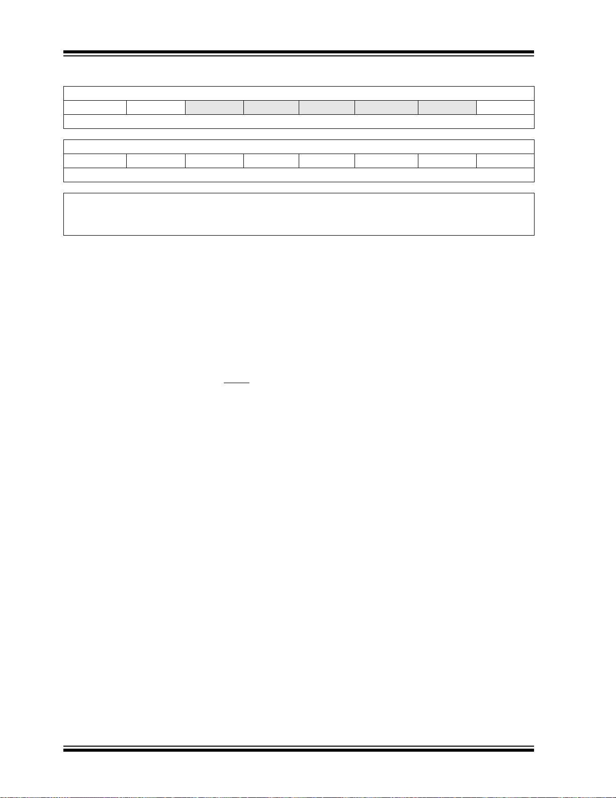
dsPIC33FJXXXGPX06/X08/X10
REGISTER 6-1: RCON: RESET CONTROL REGISTER
R/W-0 R/W-0 U-0 U-0 U-0 U-0 U-0 R/W-0
TRAPR IOPUWR
bit 15 bit 8
R/W-0 R/W-0 R/W-0 R/W-0 R/W-0 R/W-0 R/W-1 R/W-1
EXTR SWR SWDTEN
bit 7 bit 0
Legend:
R = Readable bit W = Writable bit U = Unimplemented bit, read as ‘0’
-n = Value at POR ‘1’ = Bit is set ‘0’ = Bit is cleared x = Bit is unknown
bit 15 TRAPR: Trap Reset Flag bit
1 = A Trap Conflict Reset has occurred
0 = A Trap Conflict Reset has not occurred
bit 14 IOPUWR: Illegal Opcode or Uninitialized W Access Reset Flag bit
1 = An illegal opcode detection, an illegal address mode or uninitialized W register used as an
Address Pointer caused a Reset
0 = An illegal opcode or uninitialized W Reset has not occurred
bit 13-9 Unimplemented: Read as ‘0’
bit 8 VREGS: Voltage Regulator Standby During Sleep bit
1 = Voltage regulator is active during Sleep
0 = Voltage regulator goes into Standby mode during Sleep
bit 7 EXTR: External Reset (MCLR
1 = A Master Clear (pin) Reset has occurred
0 = A Master Clear (pin) Reset has not occurred
bit 6 SWR: Software Reset (Instruction) Flag bit
1 = A RESET instruction has been executed
0 = A RESET instruction has not been executed
bit 5 SWDTEN: Software Enable/Disable of WDT bit
1 = WDT is enabled
0 = WDT is disabled
bit 4 WDTO: Watchdog Timer Time-out Flag bit
1 = WDT time-out has occurred
0 = WDT time-out has not occurred
bit 3 SLEEP: Wake-up from Sleep Flag bit
1 = Device has been in Sleep mode
0 = Device has not been in Sleep mode
bit 2 IDLE: Wake-up from Idle Flag bit
1 = Device was in Idle mode
0 = Device was not in Idle mode
bit 1 BOR: Brown-out Reset Flag bit
1 = A Brown-out Reset has occurred
0 = A Brown-out Reset has not occurred
bit 0 POR: Power-on Reset Flag bit
1 = A Power-on Reset has occurred
0 = A Power-on Reset has not occurred
— — — — —VREGS
(2)
WDTO SLEEP IDLE BOR POR
) Pin bit
(1)
(2)
Note 1: All of the Reset status bits may be set or cleared in software. Setting one of these bits in software does not
cause a device Reset.
2: If the FWDTEN Configuration bit is ‘1’ (unprogrammed), the WDT is always enabled, regardless of the
SWDTEN bit setting.
DS70286C-page 78 © 2009 Microchip Technology Inc.

dsPIC33FJXXXGPX06/X08/X10
TABLE 6-1: RESET FLAG BIT OPERATION
Flag Bit Setting Event Clearing Event
TRAPR (RCON<15>) Trap conflict event POR, BOR
IOPUWR (RCON<14>) Illegal opcode or uninitialized
W register access
EXTR (RCON<7>) MCLR
SWR (RCON<6>) RESET instruction POR, BOR
WDTO (RCON<4>) WDT time-out PWRSAV instruction, POR, BOR
SLEEP (RCON<3>) PWRSAV #SLEEP instruction POR, BOR
IDLE (RCON<2>) PWRSAV #IDLE instruction POR, BOR
BOR (RCON<1>) BOR, POR —
POR (RCON<0>) POR —
Note: All Reset flag bits may be set or cleared by the user software.
Reset POR
POR, BOR
6.1 Clock Source Selection at Reset
If clock switching is enabled, the system clock source at
device Reset is chosen, as shown in Table 6-2. If clock
switching is disabled, the system clock source is always
selected according to the oscillator Configuration bits.
Refer to Section 9.0 “Oscillator Configuration” for
further details.
TABLE 6-2: OSCILLATOR SELECTION VS
TYPE OF RESET (CLOCK
SWITCHING ENABLED)
Reset Type Clock Source Determinant
POR Oscillator Configuration bits
BOR
MCLR
WDTR
SWR
(FNOSC<2:0>)
COSC Control bits
(OSCCON<14:12>)
6.2 Device Reset Times
The Reset times for various types of device Reset are
summarized in Table 6-3. The system Reset signal,
SYSRST
times expire.
The time at which the device actually begins to execute
code also depends on the system oscillator delays,
which include the Oscillator Start-up Timer (OST) and
the PLL lock time. The OST and PLL lock times occur
in parallel with the applicable SYSRST
The FSCM delay determines the time at which the
FSCM begins to monitor the system clock source after
the SYSRST
, is released after the POR and PWRT delay
delay times.
signal is released.
© 2009 Microchip Technology Inc. DS70286C-page 79
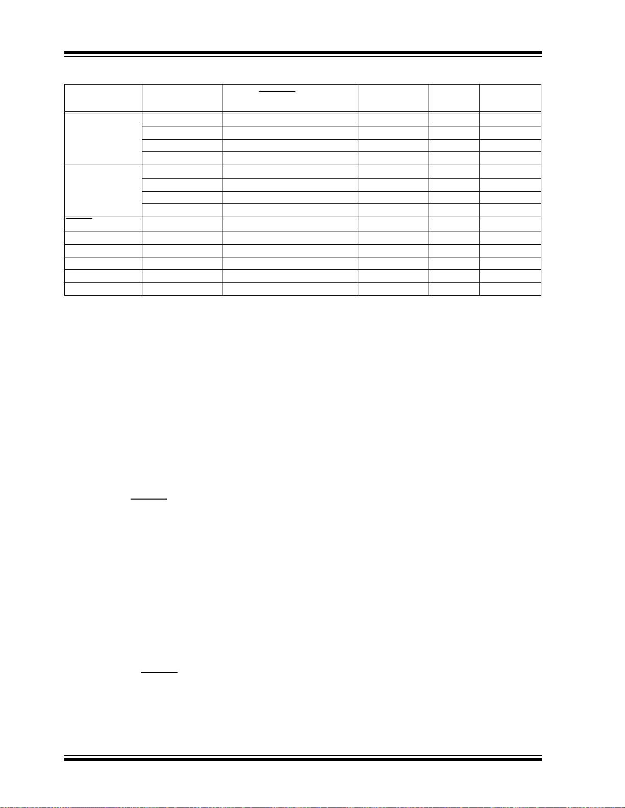
dsPIC33FJXXXGPX06/X08/X10
TABLE 6-3: RESET DELAY TIMES FOR VARIOUS DEVICE RESETS
Reset Type Clock Source SYSRST
POR EC, FRC, LPRC T
ECPLL, FRCPLL T
XT, HS, SOSC T
XTPLL, HSPLL T
POR
POR
POR
POR
Delay
+ TSTARTUP + TRST ——1, 2, 3
+ TSTARTUP + TRST TLOCK TFSCM 1, 2, 3, 5, 6
+ TSTARTUP + TRST TOST TFSCM 1, 2, 3, 4, 6
+ TSTARTUP + TRST TOST + TLOCK TFSCM 1, 2, 3, 4, 5, 6
System Clock
Delay
BOR EC, FRC, LPRC TSTARTUP + TRST ——3
ECPLL, FRCPLL T
XT, HS, SOSC T
XTPLL, HSPLL T
MCLR
Any Clock TRST ——3
WDT Any Clock T
Software Any Clock T
Illegal Opcode Any Clock T
Uninitialized W Any Clock T
Trap Conflict Any Clock T
Note 1: T
POR = Power-on Reset delay (10 μs nominal).
2: T
STARTUP = Conditional POR delay of 20 μs nominal (if on-chip regulator is enabled) or 64 ms nominal
Power-up Timer delay (if regulator is disabled). T
STARTUP + TRST TLOCK TFSCM 3, 5, 6
STARTUP + TRST TOST TFSCM 3, 4, 6
STARTUP + TRST TOST + TLOCK TFSCM 3, 4, 5, 6
RST ——3
RST ——3
RST ——3
RST ——3
RST ——3
STARTUP is also applied to all returns from powered-down
states, including waking from Sleep mode, only if the regulator is enabled.
3: T
RST = Internal state Reset time (20 μs nominal).
4: T
OST = Oscillator Start-up Timer. A 10-bit counter counts 1024 oscillator periods before releasing the
oscillator clock to the system.
5: T
LOCK = PLL lock time (20 μs nominal).
6: TFSCM = Fail-Safe Clock Monitor delay (100 μs nominal).
FSCM
Delay
Notes
6.2.1 POR AND LONG OSCILLATOR START-UP TIMES
The oscillator start-up circuitry and its associated delay
timers are not linked to the device Reset delays that
occur at power-up. Some crystal circuits (especially
low-frequency crystals) have a relatively long start-up
time. Therefore, one or more of the following conditions
is possible after SYSRST
is released:
• The oscillator circuit has not begun to oscillate.
• The Oscillator Start-up Timer has not expired (if a
crystal oscillator is used).
• The PLL has not achieved a lock (if PLL is used).
The device will not begin to execute code until a valid
clock source has been released to the system.
Therefore, the oscillator and PLL start-up delays must
be considered when the Reset delay time must be
known.
6.2.2 FAIL-SAFE CLOCK MONITOR (FSCM) AND DEVICE RESETS
If the FSCM is enabled, it begins to monitor the system
clock source when SYSRST
source is not available at this time, the device
automatically switches to the FRC oscillator and the
user can switch to the desired crystal oscillator in the
Trap Service Routine.
is released. If a valid clock
6.2.2.1 FSCM Delay for Crystal and PLL
Clock Sources
When the system clock source is provided by a crystal
oscillator and/or the PLL, a small delay, T
FSCM, is auto-
matically inserted after the POR and PWRT delay
times. The FSCM does not begin to monitor the system
clock source until this delay expires. The FSCM delay
time is nominally 500 μs and provides additional time
for the oscillator and/or PLL to stabilize. In most cases,
the FSCM delay prevents an oscillator failure trap at a
device Reset when the PWRT is disabled.
6.3 Special Function Register Reset
States
Most of the Special Function Registers (SFRs) associated with the CPU and peripherals are reset to a
particular value at a device Reset. The SFRs are
grouped by their peripheral or CPU function and their
Reset values are specified in each section of this manual.
The Reset value for each SFR does not depend on the
type of Reset, with the exception of two registers. The
Reset value for the Reset Control register, RCON,
depends on the type of device Reset. The Reset value
for the Oscillator Control register, OSCCON, depends
on the type of Reset and the programmed values of the
oscillator Configuration bits in the FOSC Configuration
register.
DS70286C-page 80 © 2009 Microchip Technology Inc.

dsPIC33FJXXXGPX06/X08/X10
7.0 INTERRUPT CONTROLLER
Note: This data sheet summarizes the features
of the dsPIC33FJXXXGPX06/X08/X10
family of devices. However, it is not
intended to be a comprehensive reference
source. To complement the information in
this data sheet, refer to Section 6.
“Interrupts” (DS70184) in the “dsPIC33F
Family Reference Manual”, which is avail-
able from the Microchip web site
(www.microchip.com).
The dsPIC33FJXXXGPX06/X08/X10 interrupt
controller reduces the numerous peripheral interrupt
request signals to a single interrupt request signal to
the dsPIC33FJXXXGPX06/X08/X10 CPU. It has the
following features:
• Up to 8 processor exceptions and software traps
• 7 user-selectable priority levels
• Interrupt Vector Table (IVT) with up to 118 vectors
• A unique vector for each interrupt or exception
source
• Fixed priority within a specified user priority level
• Alternate Interrupt Vector Table (AIVT) for debug
support
• Fixed interrupt entry and return latencies
7.1.1 ALTERNATE VECTOR TABLE
The Alternate Interrupt Vector Table (AIVT) is located
after the IVT, as shown in Figure 7-1. Access to the
AIVT is provided by the ALTIVT control bit
(INTCON2<15>). If the ALTIVT bit is set, all interrupt
and exception processes use the alternate vectors
instead of the default vectors. The alternate vectors are
organized in the same manner as the default vectors.
The AIVT supports debugging by providing a means to
switch between an application and a support
environment without requiring the interrupt vectors to
be reprogrammed. This feature also enables switching
between applications for evaluation of different
software algorithms at run time. If the AIVT is not
needed, the AIVT should be programmed with the
same addresses used in the IVT.
7.2 Reset Sequence
A device Reset is not a true exception because the
interrupt controller is not involved in the Reset process.
The dsPIC33FJXXXGPX06/X08/X10 device clears its
registers in response to a Reset, which forces the PC
to zero. The digital signal controller then begins
program execution at location 0x000000. The user
programs a GOTO instruction at the Reset address
which redirects program execution to the appropriate
start-up routine.
7.1 Interrupt Vector Table
The Interrupt Vector Table is shown in Figure 7-1. The
IVT resides in program memory, starting at location
000004h. The IVT contains 126 vectors consisting of
8 nonmaskable trap vectors plus up to 118 sources of
interrupt. In general, each interrupt source has its own
vector. Each interrupt vector contains a 24-bit wide
address. The value programmed into each interrupt
vector location is the starting address of the associated
Interrupt Service Routine (ISR).
Interrupt vectors are prioritized in terms of their natural
priority; this priority is linked to their position in the
vector table. All other things being equal, lower
addresses have a higher natural priority. For example,
the interrupt associated with vector 0 will take priority
over interrupts at any other vector address.
dsPIC33FJXXXGPX06/X08/X10 devices implement up
to 67 unique interrupts and 5 nonmaskable traps.
These are summarized in Table 7-1 and Table 7-2.
Note: Any unimplemented or unused vector
locations in the IVT and AIVT should be
programmed with the address of a default
interrupt handler routine that contains a
RESET instruction.
© 2009 Microchip Technology Inc. DS70286C-page 81
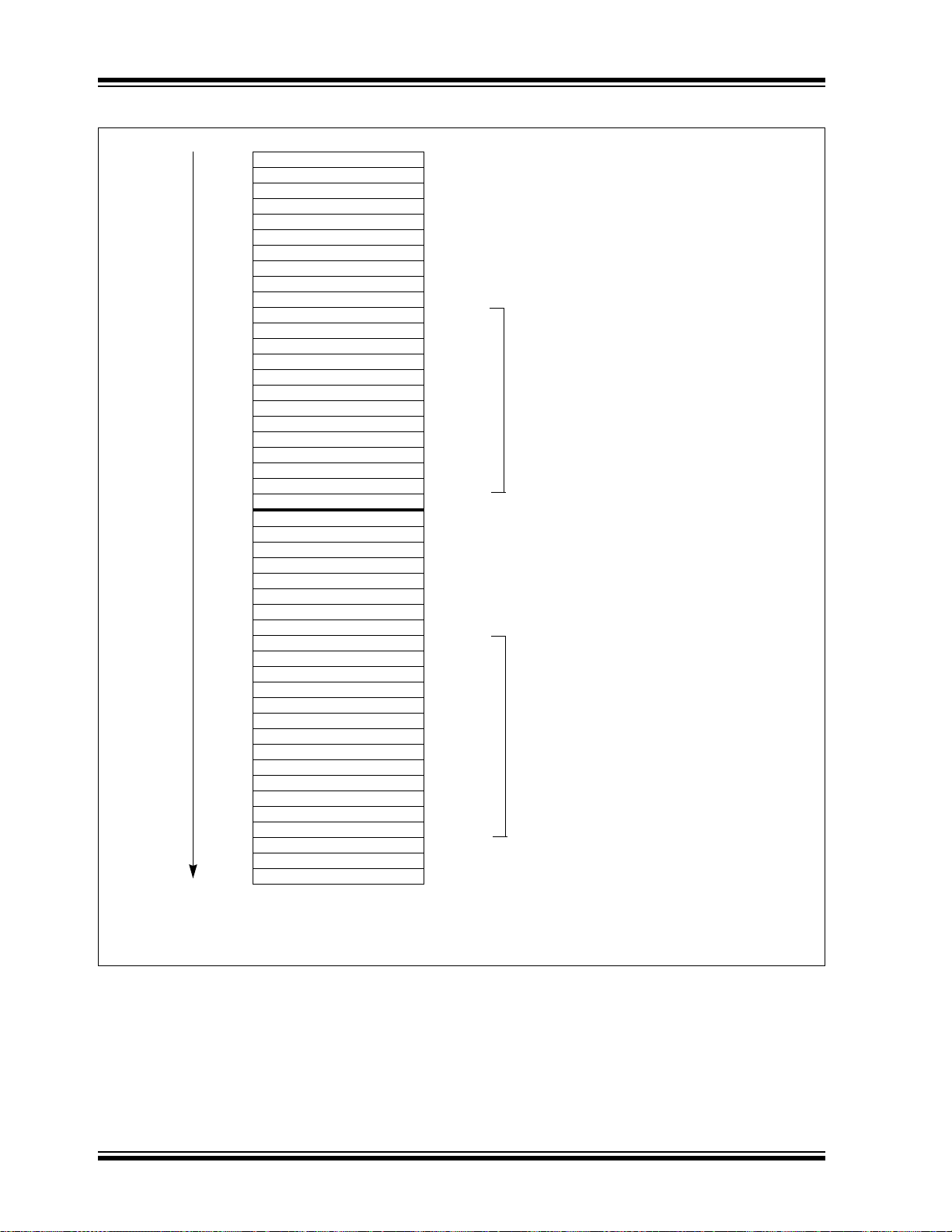
dsPIC33FJXXXGPX06/X08/X10
Reset – GOTO Instruction 0x000000
Reset – GOTO Address 0x000002
Reserved 0x000004
Oscillator Fail Trap Vector
Address Error Trap Vector
Stack Error Trap Vector
Math Error Trap Vector
DMA Error Trap Vector
Reserved
Reserved
Interrupt Vector 0 0x000014
Interrupt Vector 1
~
~
~
Interrupt Vector 52 0x00007C
Interrupt Vector 53 0x00007E
Interrupt Vector 54 0x000080
~
~
~
Interrupt Vector 116 0x0000FC
Interrupt Vector 117 0x0000FE
Reserved
0x000100
Reserved 0x000102
Reserved
Oscillator Fail Trap Vector
Address Error Trap Vector
Stack Error Trap Vector
Math Error Trap Vector
DMA Error Trap Vector
Reserved
Reserved
Interrupt Vector 0 0x000114
Interrupt Vector 1
~
~
~
Interrupt Vector 52 0x00017C
Interrupt Vector 53 0x00017E
Interrupt Vector 54 0x000180
~
~
~
Interrupt Vector 116
Interrupt Vector 117 0x0001FE
Start of Code 0x000200
Decreasing Natural Order Priority
Interrupt Vector Table (IVT)
(1)
Alternate Interrupt Vector Table (AIVT)
(1)
Note 1: See Table 7-1 for the list of implemented interrupt vectors.
FIGURE 7-1: dsPIC33FJXXXGPX06/X08/X10 INTERRUPT VECTOR TABLE
DS70286C-page 82 © 2009 Microchip Technology Inc.

dsPIC33FJXXXGPX06/X08/X10
TABLE 7-1: INTERRUPT VECTORS
Vector
Number
8 0 0x000014 0x000114 INT0 – External Interrupt 0
9 1 0x000016 0x000116 IC1 – Input Compare 1
10 2 0x000018 0x000118 OC1 – Output Compare 1
11 3 0x00001A 0x00011A T1 – Timer1
12 4 0x00001C 0x00011C DMA0 – DMA Channel 0
13 5 0x00001E 0x00011E IC2 – Input Capture 2
14 6 0x000020 0x000120 OC2 – Output Compare 2
15 7 0x000022 0x000122 T2 – Timer2
16 8 0x000024 0x000124 T3 – Timer3
17 9 0x000026 0x000126 SPI1E – SPI1 Error
18 10 0x000028 0x000128 SPI1 – SPI1 Transfer Done
19 11 0x00002A 0x00012A U1RX – UART1 Receiver
20 12 0x00002C 0x00012C U1TX – UART1 Transmitter
21 13 0x00002E 0x00012E ADC1 – ADC 1
22 14 0x000030 0x000130 DMA1 – DMA Channel 1
23 15 0x000032 0x000132 Reserved
24 16 0x000034 0x000134 SI2C1 – I2C1 Slave Events
25 17 0x000036 0x000136 MI2C1 – I2C1 Master Events
26 18 0x000038 0x000138 Reserved
27 19 0x00003A 0x00013A Change Notification Interrupt
28 20 0x00003C 0x00013C INT1 – External Interrupt 1
29 21 0x00003E 0x00013E ADC2 – ADC 2
30 22 0x000040 0x000140 IC7 – Input Capture 7
31 23 0x000042 0x000142 IC8 – Input Capture 8
32 24 0x000044 0x000144 DMA2 – DMA Channel 2
33 25 0x000046 0x000146 OC3 – Output Compare 3
34 26 0x000048 0x000148 OC4 – Output Compare 4
35 27 0x00004A 0x00014A T4 – Timer4
36 28 0x00004C 0x00014C T5 – Timer5
37 29 0x00004E 0x00014E INT2 – External Interrupt 2
38 30 0x000050 0x000150 U2RX – UART2 Receiver
39 31 0x000052 0x000152 U2TX – UART2 Transmitter
40 32 0x000054 0x000154 SPI2E – SPI2 Error
41 33 0x000056 0x000156 SPI1 – SPI1 Transfer Done
42 34 0x000058 0x000158 C1RX – ECAN1 Receive Data Ready
43 35 0x00005A 0x00015A C1 – ECAN1 Event
44 36 0x00005C 0x00015C DMA3 – DMA Channel 3
45 37 0x00005E 0x00015E IC3 – Input Capture 3
46 38 0x000060 0x000160 IC4 – Input Capture 4
47 39 0x000062 0x000162 IC5 – Input Capture 5
48 40 0x000064 0x000164 IC6 – Input Capture 6
49 41 0x000066 0x000166 OC5 – Output Compare 5
50 42 0x000068 0x000168 OC6 – Output Compare 6
51 43 0x00006A 0x00016A OC7 – Output Compare 7
52 44 0x00006C 0x00016C OC8 – Output Compare 8
53 45 0x00006E 0x00016E Reserved
Interrupt
Request (IRQ)
Number
IVT Address AIVT Address Interrupt Source
© 2009 Microchip Technology Inc. DS70286C-page 83
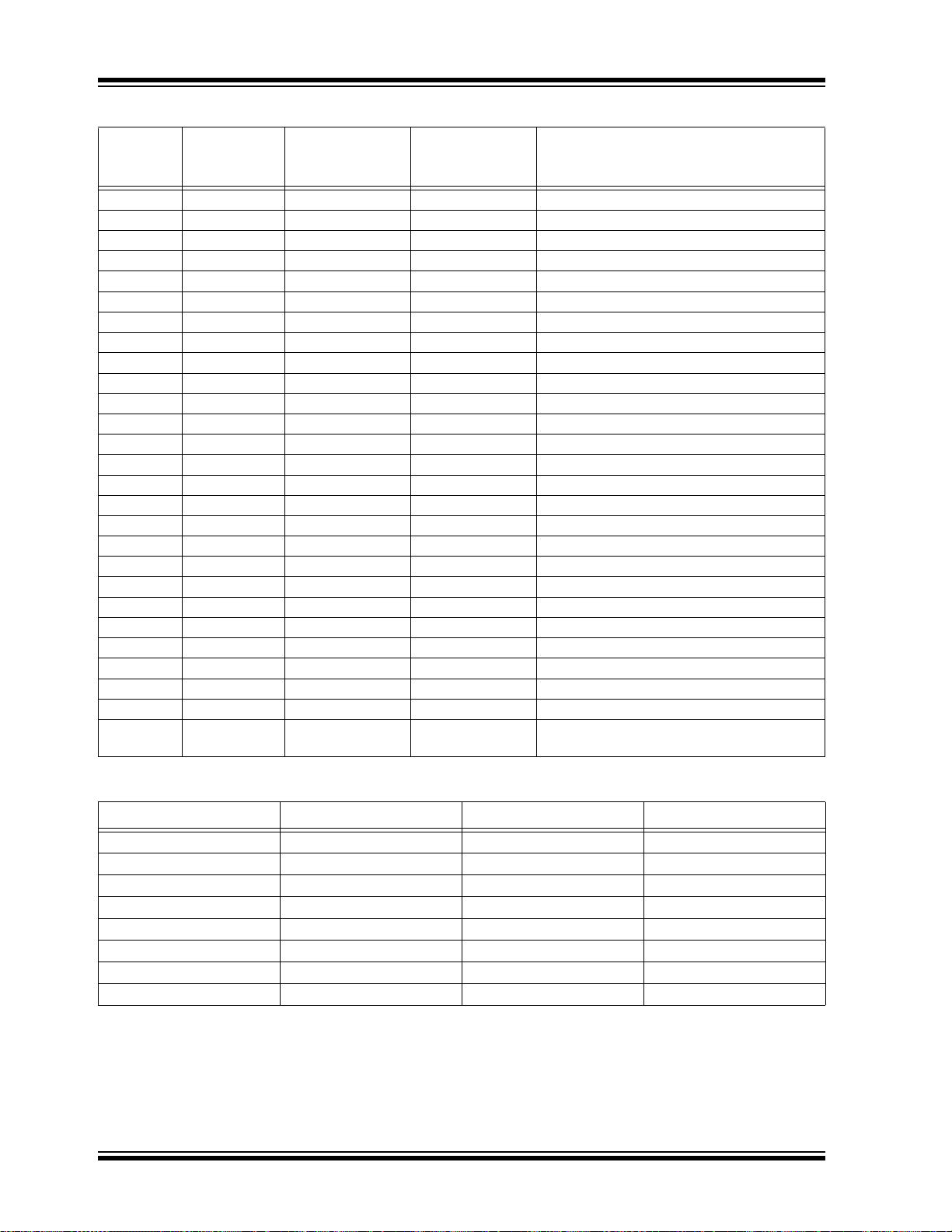
dsPIC33FJXXXGPX06/X08/X10
TABLE 7-1: INTERRUPT VECTORS (CONTINUED)
Vector
Number
54 46 0x000070 0x000170 DMA4 – DMA Channel 4
55 47 0x000072 0x000172 T6 – Timer6
56 48 0x000074 0x000174 T7 – Timer7
57 49 0x000076 0x000176 SI2C2 – I2C2 Slave Events
58 50 0x000078 0x000178 MI2C2 – I2C2 Master Events
59 51 0x00007A 0x00017A T8 – Timer8
60 52 0x00007C 0x00017C T9 – Timer9
61 53 0x00007E 0x00017E INT3 – External Interrupt 3
62 54 0x000080 0x000180 INT4 – External Interrupt 4
63 55 0x000082 0x000182 C2RX – ECAN2 Receive Data Ready
64 56 0x000084 0x000184 C2 – ECAN2 Event
65 57 0x000086 0x000186 Reserved
66 58 0x000088 0x000188 Reserved
67 59 0x00008A 0x00018A DCIE – DCI Error
68 60 0x00008C 0x00018C DCID – DCI Transfer Done
69 61 0x00008E 0x00018E DMA5 – DMA Channel 5
70 62 0x000090 0x000190 Reserved
71 63 0x000092 0x000192 Reserved
72 64 0x000094 0x000194 Reserved
73 65 0x000096 0x000196 U1E – UART1 Error
74 66 0x000098 0x000198 U2E – UART2 Error
75 67 0x00009A 0x00019A Reserved
76 68 0x00009C 0x00019C DMA6 – DMA Channel 6
77 69 0x00009E 0x00019E DMA7 – DMA Channel 7
78 70 0x0000A0 0x0001A0 C1TX – ECAN1 Transmit Data Request
79 71 0x0000A2 0x0001A2 C2TX – ECAN2 Transmit Data Request
80-125 72-117 0x0000A4-0x0000FE0x0001A4-0x0001FEReserved
Interrupt
Request (IRQ)
Number
IVT Address AIVT Address Interrupt Source
TABLE 7-2: TRAP VECTORS
Vector Number IVT Address AIVT Address Trap Source
0 0x000004 0x000104 Reserved
1 0x000006 0x000106 Oscillator Failure
2 0x000008 0x000108 Address Error
3 0x00000A 0x00010A Stack Error
4 0x00000C 0x00010C Math Error
5 0x00000E 0x00010E DMA Error Trap
6 0x000010 0x000110 Reserved
7 0x000012 0x000112 Reserved
DS70286C-page 84 © 2009 Microchip Technology Inc.

dsPIC33FJXXXGPX06/X08/X10
7.3 Interrupt Control and Status Registers
dsPIC33FJXXXGPX06/X08/X10 devices implement a
total of 30 registers for the interrupt controller:
• INTCON1
• INTCON2
• IFS0 through IFS4
• IEC0 through IEC4
• IPC0 through IPC17
•INTTREG
Global interrupt control functions are controlled from
INTCON1 and INTCON2. INTCON1 contains the
Interrupt Nesting Disable (NSTDIS) bit as well as the
control and status flags for the processor trap sources.
The INTCON2 register controls the external interrupt
request signal behavior and the use of the Alternate
Interrupt Vector Table.
The IFS registers maintain all of the interrupt request
flags. Each source of interrupt has a Status bit, which is
set by the respective peripherals or external signal and
is cleared via software.
The IEC registers maintain all of the interrupt enable
bits. These control bits are used to individually enable
interrupts from the peripherals or external signals.
The IPC registers are used to set the interrupt priority
level for each source of interrupt. Each user interrupt
source can be assigned to one of eight priority levels.
The INTTREG register contains the associated
interrupt vector number and the new CPU interrupt
priority level, which are latched into vector number
(VECNUM<6:0>) and Interrupt level (ILR<3:0>) bit
fields in the INTTREG register. The new interrupt
priority level is the priority of the pending interrupt.
The interrupt sources are assigned to the IFSx, IECx
and IPCx registers in the same sequence that they are
listed in Table 7-1. For example, the INT0 (External
Interrupt 0) is shown as having vector number 8 and a
natural order priority of 0. Thus, the INT0IF bit is found
in IFS0<0>, the INT0IE bit in IEC0<0>, and the INT0IP
bits in the first position of IPC0 (IPC0<2:0>).
Although they are not specifically part of the interrupt
control hardware, two of the CPU Control registers
contain bits that control interrupt functionality. The CPU
STATUS register, SR, contains the IPL<2:0> bits
(SR<7:5>). These bits indicate the current CPU
interrupt priority level. The user can change the current
CPU priority level by writing to the IPL bits.
The CORCON register contains the IPL3 bit which,
together with IPL<2:0>, also indicates the current CPU
priority level. IPL3 is a read-only bit so that trap events
cannot be masked by the user software.
All Interrupt registers are described in Register 7-1
through Register 7-32, in the following pages.
© 2009 Microchip Technology Inc. DS70286C-page 85
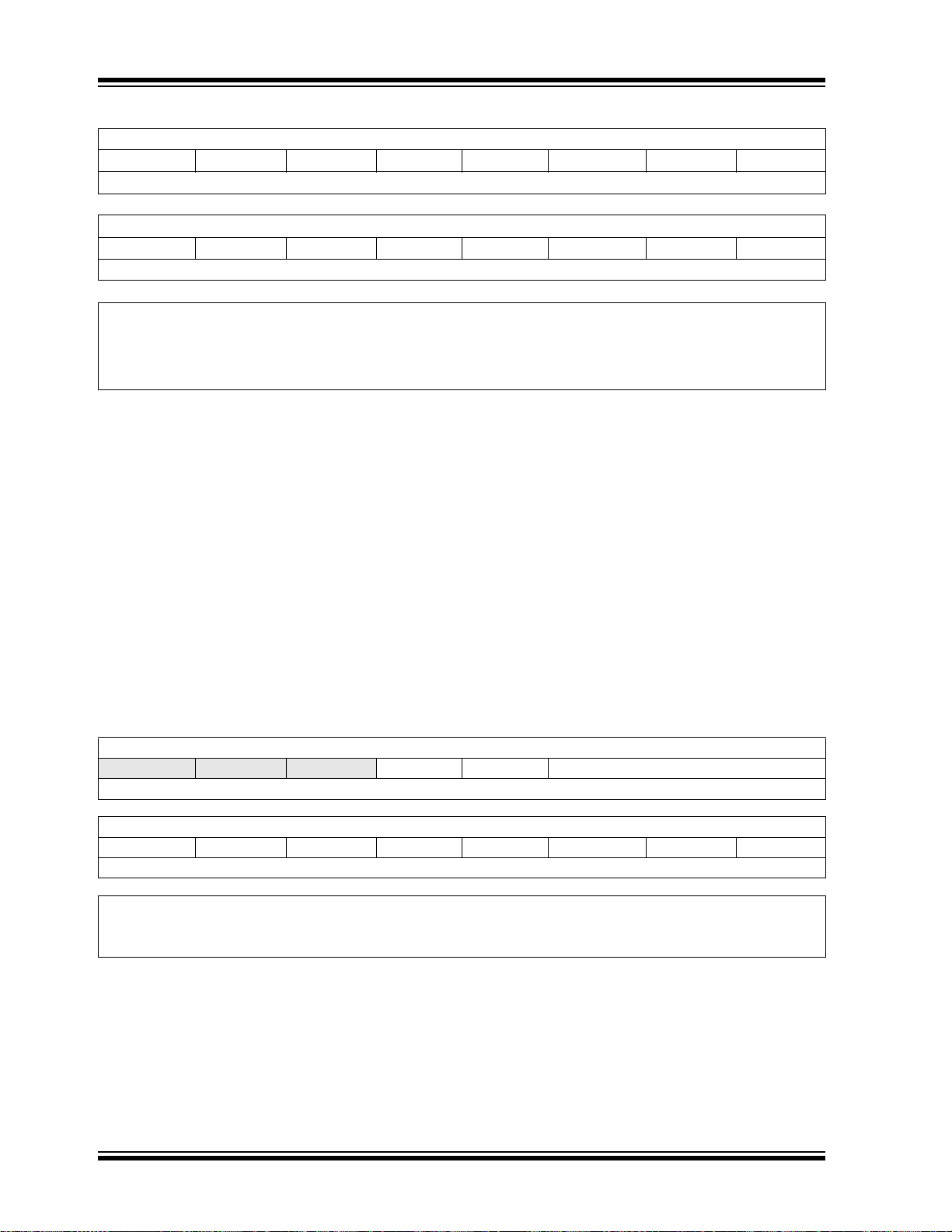
dsPIC33FJXXXGPX06/X08/X10
REGISTER 7-1: SR: CPU STATUS REGISTER
(1)
R-0 R-0 R/C-0 R/C-0 R-0 R/C-0 R -0 R/W-0
OA OB SA SB OAB SAB DA DC
bit 15 bit 8
R/W-0
IPL2
(3)
(2)
R/W-0
IPL1
(2)
(3)
R/W-0
IPL0
(2)
(3)
R-0 R/W-0 R/W-0 R/W-0 R/W-0
RA N OV Z C
bit 7 bit 0
Legend:
C = Clear only bit R = Readable bit U = Unimplemented bit, read as ‘0’
S = Set only bit W = Writable bit -n = Value at POR
‘1’ = Bit is set ‘0’ = Bit is cleared x = Bit is unknown
bit 7-5 IPL<2:0>: CPU Interrupt Priority Level Status bits
(2)
111 = CPU Interrupt Priority Level is 7 (15), user interrupts disabled
110 = CPU Interrupt Priority Level is 6 (14)
101 = CPU Interrupt Priority Level is 5 (13)
100 = CPU Interrupt Priority Level is 4 (12)
011 = CPU Interrupt Priority Level is 3 (11)
010 = CPU Interrupt Priority Level is 2 (10)
001 = CPU Interrupt Priority Level is 1 (9)
000 = CPU Interrupt Priority Level is 0 (8)
Note 1: For complete register details, see Register 3-1: “SR: CPU STATUS REGISTER”.
2: The IPL<2:0> bits are concatenated with the IPL<3> bit (CORCON<3>) to form the CPU Interrupt Priority
Level. The value in parentheses indicates the IPL if IPL<3> = 1. User interrupts are disabled when
IPL<3> = 1.
3: The IPL<2:0> Status bits are read-only when NSTDIS (INTCON1<15>) = 1.
REGISTER 7-2: CORCON: CORE CONTROL REGISTER
(1)
U-0 U-0 U-0 R/W-0 R/W-0 R-0 R-0 R-0
— — —USEDT DL<2:0>
bit 15 bit 8
R/W-0 R/W-0 R/W-1 R/W-0 R/C-0 R/W-0 R/W-0 R/W-0
SATA SATB SATDW ACCSAT IPL3
(2)
PSV RND IF
bit 7 bit 0
Legend: C = Clear only bit
R = Readable bit W = Writable bit -n = Value at POR ‘1’ = Bit is set
0’ = Bit is cleared ‘x = Bit is unknown U = Unimplemented bit, read as ‘0’
bit 3 IPL3: CPU Interrupt Priority Level Status bit 3
(2)
1 = CPU interrupt priority level is greater than 7
0 = CPU interrupt priority level is 7 or less
Note 1: For complete register details, see Register 3-2: “CORCON: CORE CONTROL REGISTER”.
2: The IPL3 bit is concatenated with the IPL<2:0> bits (SR<7:5>) to form the CPU Interrupt Priority Level.
DS70286C-page 86 © 2009 Microchip Technology Inc.

dsPIC33FJXXXGPX06/X08/X10
REGISTER 7-3: INTCON1: INTERRUPT CONTROL REGISTER 1
R/W-0 R/W-0 R/W-0 R/W-0 R/W-0 R/W-0 R/W-0 R/W-0
NSTDIS OVAERR OVBERR COVAERR COVBERR OVATE OVBTE COVTE
bit 15 bit 8
R/W-0 R/W-0 R/W-0 R/W-0 R/W-0 R/W-0 R/W-0 U-0
SFTACERR DIV0ERR DMACERR MATHERR ADDRERR STKERR OSCFAIL
bit 7 bit 0
Legend:
R = Readable bit W = Writable bit U = Unimplemented bit, read as ‘0’
-n = Value at POR ‘1’ = Bit is set ‘0’ = Bit is cleared x = Bit is unknown
bit 15 NSTDIS: Interrupt Nesting Disable bit
1 = Interrupt nesting is disabled
0 = Interrupt nesting is enabled
bit 14 OVAERR: Accumulator A Overflow Trap Flag bit
1 = Trap was caused by overflow of Accumulator A
0 = Trap was not caused by overflow of Accumulator A
bit 13 OVBERR: Accumulator B Overflow Trap Flag bit
1 = Trap was caused by overflow of Accumulator B
0 = Trap was not caused by overflow of Accumulator B
bit 12 COVAERR: Accumulator A Catastrophic Overflow Trap Flag bit
1 = Trap was caused by catastrophic overflow of Accumulator A
0 = Trap was not caused by catastrophic overflow of Accumulator A
bit 11 COVBERR: Accumulator B Catastrophic Overflow Trap Flag bit
1 = Trap was caused by catastrophic overflow of Accumulator B
0 = Trap was not caused by catastrophic overflow of Accumulator B
bit 10 OVATE: Accumulator A Overflow Trap Enable bit
1 = Trap overflow of Accumulator A
0 = Trap disabled
bit 9 OVBTE: Accumulator B Overflow Trap Enable bit
1 = Trap overflow of Accumulator B
0 = Trap disabled
bit 8 COVTE: Catastrophic Overflow Trap Enable bit
1 = Trap on catastrophic overflow of Accumulator A or B enabled
0 = Trap disabled
bit 7 SFTACERR: Shift Accumulator Error Status bit
1 = Math error trap was caused by an invalid accumulator shift
0 = Math error trap was not caused by an invalid accumulator shift
bit 6 DIV0ERR: Arithmetic Error Status bit
1 = Math error trap was caused by a divide by zero
0 = Math error trap was not caused by a divide by zero
bit 5 DMACERR: DMA Controller Error Status bit
1 = DMA controller error trap has occurred
0 = DMA controller error trap has not occurred
bit 4 MATHERR: Arithmetic Error Status bit
1 = Math error trap has occurred
0 = Math error trap has not occurred
—
© 2009 Microchip Technology Inc. DS70286C-page 87

dsPIC33FJXXXGPX06/X08/X10
REGISTER 7-3: INTCON1: INTERRUPT CONTROL REGISTER 1 (CONTINUED)
bit 3 ADDRERR: Address Error Trap Status bit
1 = Address error trap has occurred
0 = Address error trap has not occurred
bit 2 STKERR: Stack Error Trap Status bit
1 = Stack error trap has occurred
0 = Stack error trap has not occurred
bit 1 OSCFAIL: Oscillator Failure Trap Status bit
1 = Oscillator failure trap has occurred
0 = Oscillator failure trap has not occurred
bit 0 Unimplemented: Read as ‘0’
DS70286C-page 88 © 2009 Microchip Technology Inc.

dsPIC33FJXXXGPX06/X08/X10
REGISTER 7-4: INTCON2: INTERRUPT CONTROL REGISTER 2
R/W-0 R-0 U-0 U-0 U-0 U-0 U-0 U-0
ALTIVT DISI
bit 15 bit 8
U-0 U-0 U-0 R/W-0 R/W-0 R/W-0 R/W-0 R/W-0
— — — INT4EP INT3EP INT2EP INT1EP INT0EP
bit 7 bit 0
Legend:
R = Readable bit W = Writable bit U = Unimplemented bit, read as ‘0’
-n = Value at POR ‘1’ = Bit is set ‘0’ = Bit is cleared x = Bit is unknown
bit 15 ALTIVT: Enable Alternate Interrupt Vector Table bit
1 = Use alternate vector table
0 = Use standard (default) vector table
bit 14 DISI: DISI Instruction Status bit
1 = DISI instruction is active
0 = DISI instruction is not active
bit 13-5 Unimplemented: Read as ‘0’
bit 4 INT4EP: External Interrupt 4 Edge Detect Polarity Select bit
1 = Interrupt on negative edge
0 = Interrupt on positive edge
bit 3 INT3EP: External Interrupt 3 Edge Detect Polarity Select bit
1 = Interrupt on negative edge
0 = Interrupt on positive edge
bit 2 INT2EP: External Interrupt 2 Edge Detect Polarity Select bit
1 = Interrupt on negative edge
0 = Interrupt on positive edge
bit 1 INT1EP: External Interrupt 1 Edge Detect Polarity Select bit
1 = Interrupt on negative edge
0 = Interrupt on positive edge
bit 0 INT0EP: External Interrupt 0 Edge Detect Polarity Select bit
1 = Interrupt on negative edge
0 = Interrupt on positive edge
— — — — — —
© 2009 Microchip Technology Inc. DS70286C-page 89

dsPIC33FJXXXGPX06/X08/X10
REGISTER 7-5: IFS0: INTERRUPT FLAG STATUS REGISTER 0
U-0 R/W-0 R/W-0 R/W-0 R/W-0 R/W-0 R/W-0 R/W-0
— DMA1IF AD1IF U1TXIF U1RXIF SPI1IF SPI1EIF T3IF
bit 15 bit 8
R/W-0 R/W-0 R/W-0 R/W-0 R/W-0 R/W-0 R/W-0 R/W-0
T2IF OC2IF IC2IF DMA01IF T1IF OC1IF IC1IF INT0IF
bit 7 bit 0
Legend:
R = Readable bit W = Writable bit U = Unimplemented bit, read as ‘0’
-n = Value at POR ‘1’ = Bit is set ‘0’ = Bit is cleared x = Bit is unknown
bit 15 Unimplemented: Read as ‘0’
bit 14 DMA1IF: DMA Channel 1 Data Transfer Complete Interrupt Flag Status bit
1 = Interrupt request has occurred
0 = Interrupt request has not occurred
bit 13 AD1IF: ADC1 Conversion Complete Interrupt Flag Status bit
1 = Interrupt request has occurred
0 = Interrupt request has not occurred
bit 12 U1TXIF: UART1 Transmitter Interrupt Flag Status bit
1 = Interrupt request has occurred
0 = Interrupt request has not occurred
bit 11 U1RXIF: UART1 Receiver Interrupt Flag Status bit
1 = Interrupt request has occurred
0 = Interrupt request has not occurred
bit 10 SPI1IF: SPI1 Event Interrupt Flag Status bit
1 = Interrupt request has occurred
0 = Interrupt request has not occurred
bit 9 SPI1EIF: SPI1 Fault Interrupt Flag Status bit
1 = Interrupt request has occurred
0 = Interrupt request has not occurred
bit 8 T3IF: Timer3 Interrupt Flag Status bit
1 = Interrupt request has occurred
0 = Interrupt request has not occurred
bit 7 T2IF: Timer2 Interrupt Flag Status bit
1 = Interrupt request has occurred
0 = Interrupt request has not occurred
bit 6 OC2IF: Output Compare Channel 2 Interrupt Flag Status bit
1 = Interrupt request has occurred
0 = Interrupt request has not occurred
bit 5 IC2IF: Input Capture Channel 2 Interrupt Flag Status bit
1 = Interrupt request has occurred
0 = Interrupt request has not occurred
bit 4 DMA01IF: DMA Channel 0 Data Transfer Complete Interrupt Flag Status bit
1 = Interrupt request has occurred
0 = Interrupt request has not occurred
bit 3 T1IF: Timer1 Interrupt Flag Status bit
1 = Interrupt request has occurred
0 = Interrupt request has not occurred
DS70286C-page 90 © 2009 Microchip Technology Inc.

dsPIC33FJXXXGPX06/X08/X10
REGISTER 7-5: IFS0: INTERRUPT FLAG STATUS REGISTER 0 (CONTINUED)
bit 2 OC1IF: Output Compare Channel 1 Interrupt Flag Status bit
1 = Interrupt request has occurred
0 = Interrupt request has not occurred
bit 1 IC1IF: Input Capture Channel 1 Interrupt Flag Status bit
1 = Interrupt request has occurred
0 = Interrupt request has not occurred
bit 0 INT0IF: External Interrupt 0 Flag Status bit
1 = Interrupt request has occurred
0 = Interrupt request has not occurred
© 2009 Microchip Technology Inc. DS70286C-page 91

dsPIC33FJXXXGPX06/X08/X10
REGISTER 7-6: IFS1: INTERRUPT FLAG STATUS REGISTER 1
R/W-0 R/W-0 R/W-0 R/W-0 R/W-0 R/W-0 R/W-0 R/W-0
U2TXIF U2RXIF INT2IF T5IF T4IF OC4IF OC3IF DMA21IF
bit 15 bit 8
R/W-0 R/W-0 R/W-0 R/W-0 R/W-0 U-0 R/W-0 R/W-0
IC8IF IC7IF AD2IF INT1IF CNIF
bit 7 bit 0
Legend:
R = Readable bit W = Writable bit U = Unimplemented bit, read as ‘0’
-n = Value at POR ‘1’ = Bit is set ‘0’ = Bit is cleared x = Bit is unknown
bit 15 U2TXIF: UART2 Transmitter Interrupt Flag Status bit
1 = Interrupt request has occurred
0 = Interrupt request has not occurred
bit 14 U2RXIF: UART2 Receiver Interrupt Flag Status bit
1 = Interrupt request has occurred
0 = Interrupt request has not occurred
bit 13 INT2IF: External Interrupt 2 Flag Status bit
1 = Interrupt request has occurred
0 = Interrupt request has not occurred
bit 12 T5IF: Timer5 Interrupt Flag Status bit
1 = Interrupt request has occurred
0 = Interrupt request has not occurred
bit 11 T4IF: Timer4 Interrupt Flag Status bit
1 = Interrupt request has occurred
0 = Interrupt request has not occurred
bit 10 OC4IF: Output Compare Channel 4 Interrupt Flag Status bit
1 = Interrupt request has occurred
0 = Interrupt request has not occurred
bit 9 OC3IF: Output Compare Channel 3 Interrupt Flag Status bit
1 = Interrupt request has occurred
0 = Interrupt request has not occurred
bit 8 DMA21IF: DMA Channel 2 Data Transfer Complete Interrupt Flag Status bit
1 = Interrupt request has occurred
0 = Interrupt request has not occurred
bit 7 IC8IF: Input Capture Channel 8 Interrupt Flag Status bit
1 = Interrupt request has occurred
0 = Interrupt request has not occurred
bit 6 IC7IF: Input Capture Channel 7 Interrupt Flag Status bit
1 = Interrupt request has occurred
0 = Interrupt request has not occurred
bit 5 AD2IF: ADC2 Conversion Complete Interrupt Flag Status bit
1 = Interrupt request has occurred
0 = Interrupt request has not occurred
bit 4 INT1IF: External Interrupt 1 Flag Status bit
1 = Interrupt request has occurred
0 = Interrupt request has not occurred
—MI2C1IFSI2C1IF
DS70286C-page 92 © 2009 Microchip Technology Inc.

dsPIC33FJXXXGPX06/X08/X10
REGISTER 7-6: IFS1: INTERRUPT FLAG STATUS REGISTER 1 (CONTINUED)
bit 3 CNIF: Input Change Notification Interrupt Flag Status bit
1 = Interrupt request has occurred
0 = Interrupt request has not occurred
bit 2 Unimplemented: Read as ‘0’
bit 1 MI2C1IF: I2C1 Master Events Interrupt Flag Status bit
1 = Interrupt request has occurred
0 = Interrupt request has not occurred
bit 0 SI2C1IF: I2C1 Slave Events Interrupt Flag Status bit
1 = Interrupt request has occurred
0 = Interrupt request has not occurred
© 2009 Microchip Technology Inc. DS70286C-page 93
dsPIC33FJXXXGPX06/X08/X10
REGISTER 7-7: IFS2: INTERRUPT FLAG STATUS REGISTER 2
R/W-0 R/W-0 U-0 R/W-0 R/W-0 R/W-0 R/W-0 R/W-0
T6IF DMA4IF
bit 15 bit 8
R/W-0 R/W-0 R/W-0 R/W-0 R/W-0 R/W-0 R/W-0 R/W-0
IC5IF IC4IF IC3IF DMA3IF C1IF C1RXIF SPI2IF SPI2EIF
bit 7 bit 0
Legend:
R = Readable bit W = Writable bit U = Unimplemented bit, read as ‘0’
-n = Value at POR ‘1’ = Bit is set ‘0’ = Bit is cleared x = Bit is unknown
bit 15 T6IF: Timer6 Interrupt Flag Status bit
1 = Interrupt request has occurred
0 = Interrupt request has not occurred
bit 14 DMA4IF: DMA Channel 4 Data Transfer Complete Interrupt Flag Status bit
1 = Interrupt request has occurred
0 = Interrupt request has not occurred
bit 13 Unimplemented: Read as ‘0’
bit 12 OC8IF: Output Compare Channel 8 Interrupt Flag Status bit
1 = Interrupt request has occurred
0 = Interrupt request has not occurred
bit 11 OC7IF: Output Compare Channel 7 Interrupt Flag Status bit
1 = Interrupt request has occurred
0 = Interrupt request has not occurred
bit 10 OC6IF: Output Compare Channel 6 Interrupt Flag Status bit
1 = Interrupt request has occurred
0 = Interrupt request has not occurred
bit 9 OC5IF: Output Compare Channel 5 Interrupt Flag Status bit
1 = Interrupt request has occurred
0 = Interrupt request has not occurred
bit 8 IC6IF: Input Capture Channel 6 Interrupt Flag Status bit
1 = Interrupt request has occurred
0 = Interrupt request has not occurred
bit 7 IC5IF: Input Capture Channel 5 Interrupt Flag Status bit
1 = Interrupt request has occurred
0 = Interrupt request has not occurred
bit 6 IC4IF: Input Capture Channel 4 Interrupt Flag Status bit
1 = Interrupt request has occurred
0 = Interrupt request has not occurred
bit 5 IC3IF: Input Capture Channel 3 Interrupt Flag Status bit
1 = Interrupt request has occurred
0 = Interrupt request has not occurred
bit 4 DMA3IF: DMA Channel 3 Data Transfer Complete Interrupt Flag Status bit
1 = Interrupt request has occurred
0 = Interrupt request has not occurred
bit 3 C1IF: ECAN1 Event Interrupt Flag Status bit
1 = Interrupt request has occurred
0 = Interrupt request has not occurred
— OC8IF OC7IF OC6IF OC5IF IC6IF
DS70286C-page 94 © 2009 Microchip Technology Inc.

dsPIC33FJXXXGPX06/X08/X10
REGISTER 7-7: IFS2: INTERRUPT FLAG STATUS REGISTER 2 (CONTINUED)
bit 2 C1RXIF: ECAN1 Receive Data Ready Interrupt Flag Status bit
1 = Interrupt request has occurred
0 = Interrupt request has not occurred
bit 1 SPI2IF: SPI2 Event Interrupt Flag Status bit
1 = Interrupt request has occurred
0 = Interrupt request has not occurred
bit 0 SPI2EIF: SPI2 Error Interrupt Flag Status bit
1 = Interrupt request has occurred
0 = Interrupt request has not occurred
© 2009 Microchip Technology Inc. DS70286C-page 95
dsPIC33FJXXXGPX06/X08/X10
REGISTER 7-8: IFS3: INTERRUPT FLAG STATUS REGISTER 3
U-0 U-0 R/W-0 R/W-0 R/W-0 U-0 U-0 R/W-0
— — DMA5IF DCIIF DCIEIF — —C2IF
bit 15 bit 8
R/W-0 R/W-0 R/W-0 R/W-0 R/W-0 R/W-0 R/W-0 R/W-0
C2RXIF INT4IF INT3IF T9IF T8IF MI2C2IF SI2C2IF T7IF
bit 7 bit 0
Legend:
R = Readable bit W = Writable bit U = Unimplemented bit, read as ‘0’
-n = Value at POR ‘1’ = Bit is set ‘0’ = Bit is cleared x = Bit is unknown
bit 15-14 Unimplemented: Read as ‘0’
bit 13 DMA5IF: DMA Channel 5 Data Transfer Complete Interrupt Flag Status bit
1 = Interrupt request has occurred
0 = Interrupt request has not occurred
bit 12 DCIIF: DCI Event Interrupt Flag Status bit
1 = Interrupt request has occurred
0 = Interrupt request has not occurred
bit 11 DCIEIF: DCI Error Interrupt Flag Status bit
1 = Interrupt request has occurred
0 = Interrupt request has not occurred
bit 10-9 Unimplemented: Read as ‘0’
bit 8 C2IF: ECAN2 Event Interrupt Flag Status bit
1 = Interrupt request has occurred
0 = Interrupt request has not occurred
bit 7 C2RXIF: ECAN2 Receive Data Ready Interrupt Flag Status bit
1 = Interrupt request has occurred
0 = Interrupt request has not occurred
bit 6 INT4IF: External Interrupt 4 Flag Status bit
1 = Interrupt request has occurred
0 = Interrupt request has not occurred
bit 5 INT3IF: External Interrupt 3 Flag Status bit
1 = Interrupt request has occurred
0 = Interrupt request has not occurred
bit 4 T9IF: Timer9 Interrupt Flag Status bit
1 = Interrupt request has occurred
0 = Interrupt request has not occurred
bit 3 T8IF: Timer8 Interrupt Flag Status bit
1 = Interrupt request has occurred
0 = Interrupt request has not occurred
bit 2 MI2C2IF: I2C2 Master Events Interrupt Flag Status bit
1 = Interrupt request has occurred
0 = Interrupt request has not occurred
bit 1 SI2C2IF: I2C2 Slave Events Interrupt Flag Status bit
1 = Interrupt request has occurred
0 = Interrupt request has not occurred
bit 0 T7IF: Timer7 Interrupt Flag Status bit
1 = Interrupt request has occurred
0 = Interrupt request has not occurred
DS70286C-page 96 © 2009 Microchip Technology Inc.
dsPIC33FJXXXGPX06/X08/X10
REGISTER 7-9: IFS4: INTERRUPT FLAG STATUS REGISTER 4
U-0 U-0 U-0 U-0 U-0 U-0 U-0 U-0
— — — — — — — —
bit 15 bit 8
R/W-0 R/W-0 R/W-0 R/W-0 U-0 R/W-0 R/W-0 U-0
C2TXIF C1TXIF DMA7IF DMA6IF
bit 7 bit 0
Legend:
R = Readable bit W = Writable bit U = Unimplemented bit, read as ‘0’
-n = Value at POR ‘1’ = Bit is set ‘0’ = Bit is cleared x = Bit is unknown
bit 15-8 Unimplemented: Read as ‘0’
bit 7 C2TXIF: ECAN2 Transmit Data Request Interrupt Flag Status bit
1 = Interrupt request has occurred
0 = Interrupt request has not occurred
bit 6 C1TXIF: ECAN1 Transmit Data Request Interrupt Flag Status bit
1 = Interrupt request has occurred
0 = Interrupt request has not occurred
bit 5 DMA7IF: DMA Channel 7 Data Transfer Complete Interrupt Flag Status bit
1 = Interrupt request has occurred
0 = Interrupt request has not occurred
bit 4 DMA6IF: DMA Channel 6 Data Transfer Complete Interrupt Flag Status bit
1 = Interrupt request has occurred
0 = Interrupt request has not occurred
bit 3 Unimplemented: Read as ‘0’
bit 2 U2EIF: UART2 Error Interrupt Flag Status bit
1 = Interrupt request has occurred
0 = Interrupt request has not occurred
bit 1 U1EIF: UART1 Error Interrupt Flag Status bit
1 = Interrupt request has occurred
0 = Interrupt request has not occurred
bit 0 Unimplemented: Read as ‘0’
—U2EIFU1EIF—
© 2009 Microchip Technology Inc. DS70286C-page 97

dsPIC33FJXXXGPX06/X08/X10
REGISTER 7-10: IEC0: INTERRUPT ENABLE CONTROL REGISTER 0
U-0 R/W-0 R/W-0 R/W-0 R/W-0 R/W-0 R/W-0 R/W-0
— DMA1IE AD1IE U1TXIE U1RXIE SPI1IE SPI1EIE T3IE
bit 15 bit 8
R/W-0 R/W-0 R/W-0 R/W-0 R/W-0 R/W-0 R/W-0 R/W-0
T2IE OC2IE IC2IE DMA0IE T1IE OC1IE IC1IE INT0IE
bit 7 bit 0
Legend:
R = Readable bit W = Writable bit U = Unimplemented bit, read as ‘0’
-n = Value at POR ‘1’ = Bit is set ‘0’ = Bit is cleared x = Bit is unknown
bit 15 Unimplemented: Read as ‘0’
bit 14 DMA1IE: DMA Channel 1 Data Transfer Complete Interrupt Enable bit
1 = Interrupt request enabled
0 = Interrupt request not enabled
bit 13 AD1IE: ADC1 Conversion Complete Interrupt Enable bit
1 = Interrupt request enabled
0 = Interrupt request not enabled
bit 12 U1TXIE: UART1 Transmitter Interrupt Enable bit
1 = Interrupt request enabled
0 = Interrupt request not enabled
bit 11 U1RXIE: UART1 Receiver Interrupt Enable bit
1 = Interrupt request enabled
0 = Interrupt request not enabled
bit 10 SPI1IE: SPI1 Event Interrupt Enable bit
1 = Interrupt request enabled
0 = Interrupt request not enabled
bit 9 SPI1EIE: SPI1 Error Interrupt Enable bit
1 = Interrupt request enabled
0 = Interrupt request not enabled
bit 8 T3IE: Timer3 Interrupt Enable bit
1 = Interrupt request enabled
0 = Interrupt request not enabled
bit 7 T2IE: Timer2 Interrupt Enable bit
1 = Interrupt request enabled
0 = Interrupt request not enabled
bit 6 OC2IE: Output Compare Channel 2 Interrupt Enable bit
1 = Interrupt request enabled
0 = Interrupt request not enabled
bit 5 IC2IE: Input Capture Channel 2 Interrupt Enable bit
1 = Interrupt request enabled
0 = Interrupt request not enabled
bit 4 DMA0IE: DMA Channel 0 Data Transfer Complete Interrupt Enable bit
1 = Interrupt request enabled
0 = Interrupt request not enabled
bit 3 T1IE: Timer1 Interrupt Enable bit
1 = Interrupt request enabled
0 = Interrupt request not enabled
DS70286C-page 98 © 2009 Microchip Technology Inc.
 Loading...