

Page 1
DS14C88
QUAD CMOS Line Driver
General Description
The DS14C88, pin-for-pin compatible to the DS1488/
MC1488, is a quad line drivers designed to interface data
terminal equipment (DTE) with data circuit-terminating
equipment (DCE). This device translates standard TTL/
CMOS logic levels to levels conforming to EIA-232-D and
CCITT V.28 standards.
The device is fabricated in low threshold CMOS metal gate
technology. The device provides very low power consumption compared to its bipolar equivalents: 500 µA (DS14C88)
versus 25 mA (DS1488).
The DS14C88 simplifies designs byeliminating the need for
external slew rate control capacitors. Slew rate control in accordance with EIA-232D is provided on-chip, eliminating the
output capacitors.
Features
n Meets EIA-232D and CCITT V.28 standards
n LOW power consumption
n Wide power supply range:
±
5V to±12V
n Available in SOIC package
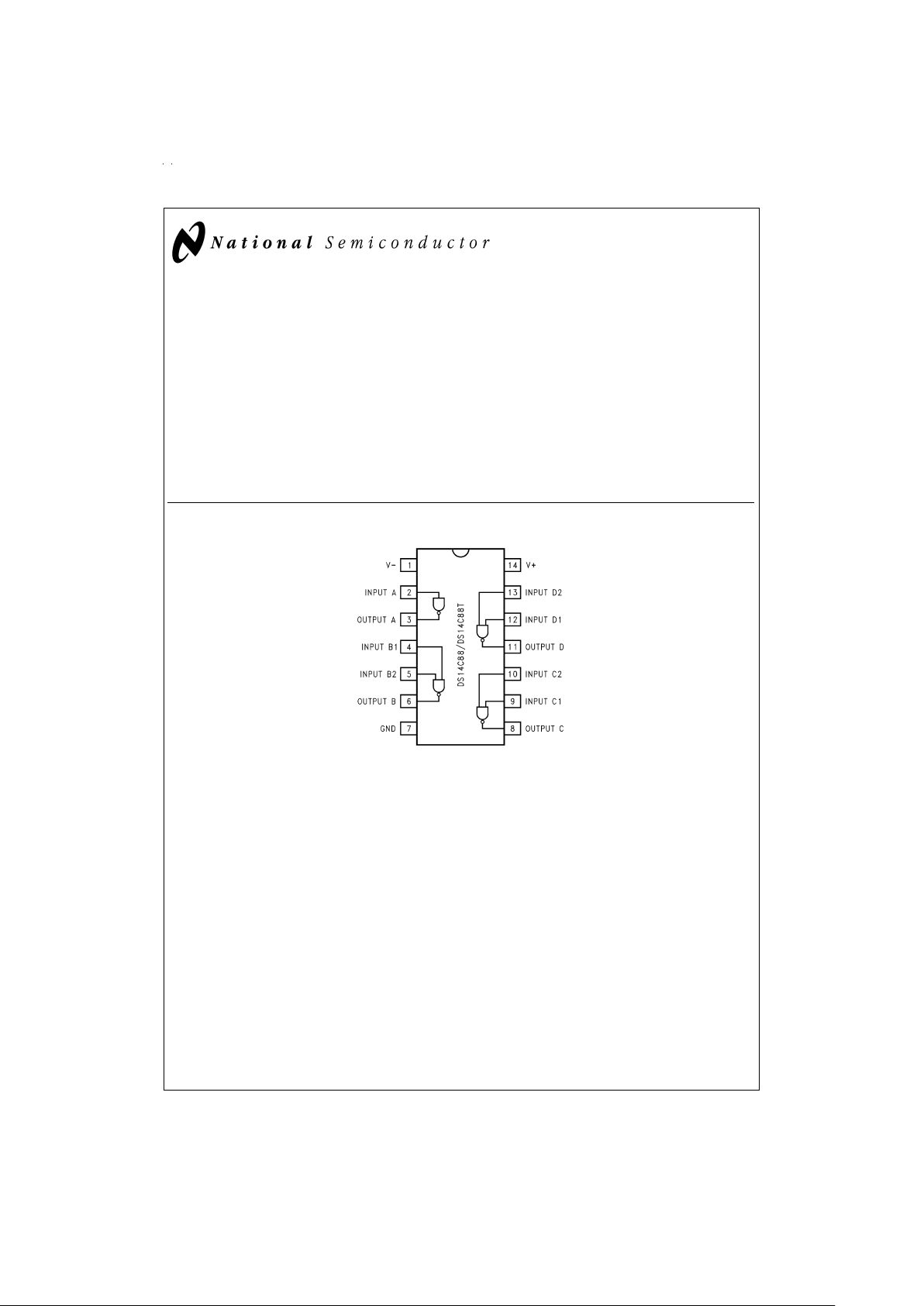
Connection Diagram
DS011105-1
Order Number DS14C88N, or DS14C88M
See NS Package Number N14A or M14A
May 1998
DS14C88 QUAD CMOS Line Driver
© 1998 National Semiconductor Corporation DS011105 www.national.com
Page 2
Absolute Maximum Ratings (Note 1)
If Military/Aerospace specified devices are required,
please contact the National Semiconductor Sales Office/
Distributors for availability and specifications.
Supply Voltage
V
+
Pin +13V
V
−
Pin −13V
Driver Input Voltage (V
+
) +0.3V to GND
−0.3V
Driver Output Voltage |(V
+
)−VO|≤30V
|(V
−
)−VO|≤30V
Continuous Power Dissipation
@
+25˚C (Note 2)
N Package 1513 mW
M Package 1063 mW
Junction Temperature +150˚C
Lead Temperature
(Soldering 4 seconds) +260˚C
Storage Temperature Range −65˚C to +150˚C
This Product does not meet 2000V ESD rating. (Note 9)
Recommended Operating
Conditions
Min Max Units
V
+
Supply (GND=0V) +4.5 +12.6 V
V
−
Supply (GND=0V) −4.5 −12.6 V
Operating Free Air Temp.
(T
A
)
DS14C88 0 +75 ˚C
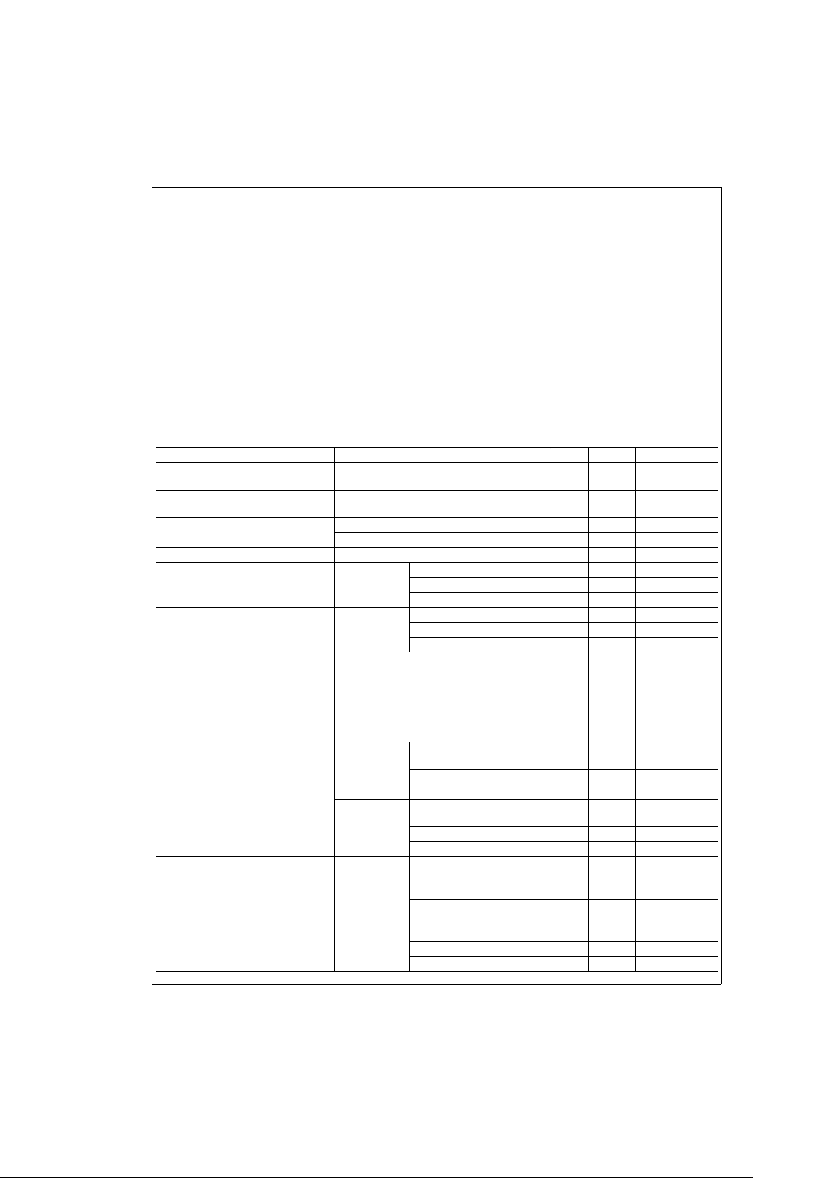
Electrical Characteristics
Over Recommended Operating Conditions, unless otherwise specified
Symbol Parameter Conditions Min Typ Max Units
I
IL
Maximum Low Input
Current
V
IN
=
GND +10 µA
I
IH
Maximum High Input
Current
V
IN
=
V
+
−10 µA
V
IL
Low Level Input Voltage V+≥ +7V, V−≤ −7V GND 0.8 V
V
+
<
+7V, V
−
>
−7V GND 0.6 V
V
IH
High Level Input Voltage 2.0 V
+
V
V
OL
Low Level Output Level V
IN
=
V
IH
V
+
=
4.5V, V
−
=
−4.5V −4.0 −3.0 V
R
L
=
3kΩ V
+
=
9V, V
−
=
9V −8.0 −6.5 V
or7kΩ V
+
=
12V, V
−
=
−12V −10.5 −9.0 V
V
OH
High Level Output Level V
IN
=
V
IL
V
+
=
4.5V, V
−
=
−4.5V 3.0 4.0 V
R
L
=
3kΩ V
+
=
9V, V
−
=
−9V 6.5 8.0 V
or7kΩ V
+
=
12V, V
−
=
−12V 9.0 10.5 V
I
OS+
High Level Output Short V
IN
=
0.8V, V
O
=
GND V
+
=
+12V, −45 mA
Circuit Current (Note 3) V
−
=
−12V
I
OS−
Low Level Output Short V
IN
=
2.0V, V
O
=
GND +45 mA
Circuit Current (Note 3)
R
OUT
Output Resistance V
+
=
V
−
=
GND=0V 300 Ω
−2V ≤ V
O
≤ +2V (Note 4) (
Figure 1
)
I
CC+
Positive Supply Current V
IN
=
V
ILmax
V
+
=
4.5V, V
−
=
−4.5V 10 µA
R
L
=
OPEN V
+
=
9V, V
−
=
−9V 30 µA
V
+
=
12V, V
−
=
−12V 60 µA
V
IN
=
V
IHmin
V
+
=
4.5V, V
−
=
−4.5V 50 µA
R
L
=
OPEN V
+
=
9V, V
−
=
−9V 300 µA
V
+
=
12V, V
−
=
−12V 500 µA
I
CC-
Negative Supply Current V
IN
=
V
ILmax
V
+
=
4.5V, V
−
=
−4.5V −10 µA
R
L
=
OPEN V
+
=
9V, V
−
=
−9V −10 µA
V
+
=
12V, V
−
=
−12V −10 µA
V
IN
=
V
IHmin
V
+
=
4.5V, V
−
=
−4.5V −30 µA
R
L
=
OPEN V
+
=
9V, V
−
=
−9V −30 µA
V
+
=
12V, V
−
=
−12V −60 µA
www.national.com 2
Page 3

Switching Characteristics (Notes 5, 6)
Over Recommended Operating Conditions, unless otheriwse specified (
Figures 2, 3
)
Symbol Parameter Conditions Min Typ Max Units
t
PLH
Propagation Delay V
+
=
+4.5V, V
−
=
−4.5V 1.5 6.0 µs
Low to High V
+
=
+9.0V, V
−
=
−9.0V 1.2 5.0 µs
V
+
=
+12V, V
−
=
−12V 1.2 4.0 µs
t
PHL
Propagation Delay V
+
=
+4.5V, V
−
=
−4.5V 1.5 6.0 µs
High to Low V
+
=
+9.0V, V
−
=
−9.0V 1.35 5.0 µs
V
+
=
+12V, V
−
=
−12V 1.3 4.0 µs
t
r
Rise Time (Note 7) 0.2 1.0 µs
t
f
Fall Time (Note 7) 0.2 1.0 µs
tsk Typical Propagation V
+
=
+4.5V, V
−
=
−4.5V 250 ns
Delay Skew V
+
=
+9.0V, V
−
=
−9.0V 200 ns
V
+
=
+12V, V
−
=
−12V 150 ns
S
R
Output Slew Rate R
L
=
3kΩto7kΩ 30 V/µs
(Note 7) C
L
=
15 pF to 2500 pF
Note 1: “Absolute Maximum Ratings” are those values beyond which the safety of the device cannot be guaranteed. They are not meant to imply that the devices
should be operated at these limits. The tables of “Electrical Characteristics” specify conditions for device operation.
Note 2: Derate N Package 12.1 mW/˚C, and M Package 8.5 mW/˚C above +25˚C.
Note 3: I
OS+
and I
OS−
values are for one output at a time. If more than one output is shorted simultaneously, the device dissipation may be exceeded.
Note 4: Power supply (V
+,V−
) and GND pins are connected to ground for the Output Resistance Test (RO).
Note 5: AC input test waveforms for test purposes: t
r
=
t
f
≤ 20 ns, V
IH
=
2V, V
IL
=
0.8V (0.6V at V
+
=
4.5V, V
−
=
−4.5V)
Note 6: Input rise and rall times must not exceed 5 µs.
Note 7: The output slew rate, rise time, and fall time are measured from the +3.0V to the −3.0V level on the output waveform.
Note 8: C
L
include jig and probe capacitances.
Note 9: ESD Rating (HBM, 1.5 kΩ, 100 pF) ≥ 1.0 kV.
Parameter Measure Information
DS011105-2
FIGURE 1. Output Resistance Test Circuit (Power-Off)
DS011105-3
FIGURE 2. Driver Load Circuit (Note 8)
www.national.com3
Page 4

Parameter Measure Information (Continued)
Typical Application Information
DS011105-4
FIGURE 3. Driver Switching Waveform
DS011105-5
FIGURE 4. EIA-232D Data Transmission
www.national.com 4
Page 5

Physical Dimensions inches (millimeters) unless otherwise noted
Order Number DS14C88M or DS14C88TM
NS Package Number M14A
Order Number DS14C88N or DS14C88TN
NS Package Number N14A
www.national.com5
Page 6

LIFE SUPPORT POLICY
NATIONAL’S PRODUCTS ARE NOT AUTHORIZED FOR USE AS CRITICAL COMPONENTS IN LIFE SUPPORT DEVICES OR SYSTEMS WITHOUT THE EXPRESS WRITTEN APPROVAL OF THE PRESIDENT OF NATIONAL SEMICONDUCTOR CORPORATION. As used herein:
1. Life support devices or systems are devices or systems which, (a) are intended for surgical implant into
the body, or (b) support or sustain life, and whose failure to perform when properly used in accordance
with instructions for use provided in the labeling, can
be reasonably expected to result in a significant injury
to the user.
2. A critical component in any component of a life support
device or system whose failure to perform can be reasonably expected to cause the failure of the life support
device or system, or to affect its safety or effectiveness.
National Semiconductor
Corporation
Americas
Tel: 1-800-272-9959
Fax: 1-800-737-7018
Email: support@nsc.com
www.national.com
National Semiconductor
Europe
Fax: +49 (0) 1 80-530 85 86
Email: europe.support@nsc.com
Deutsch Tel: +49 (0) 1 80-530 85 85
English Tel: +49 (0) 1 80-532 78 32
Français Tel: +49 (0) 1 80-532 93 58
Italiano Tel: +49 (0) 1 80-534 16 80
National Semiconductor
Asia Pacific Customer
Response Group
Tel: 65-2544466
Fax: 65-2504466
Email: sea.support@nsc.com
National Semiconductor
Japan Ltd.
Tel: 81-3-5620-6175
Fax: 81-3-5620-6179
DS14C88 QUAD CMOS Line Driver
National does not assume any responsibility for use of any circuitry described, no circuit patent licenses are implied and National reserves the right at any time without notice to change said circuitry and specifications.
 Loading...