

Page 1
DS1385/DS1387
DS1385/DS1387
RAMified Real Time Clock 4K x 8
FEATURES
• Upgraded IBM AT computer clock/calendar with
4K x 8 extended RAM
• Totally nonvolatile with over 10 years of operation in
the absence of power
• Counts seconds, minutes, hours, day of the week,
date, month and year with leap year compensation
• Binary or BCD representations of time, calendar and
alarm
• 12– or 24–hour clock with AM and PM in 12–hour
mode
• Daylight Savings Time option
• Multiplex bus for pin efficiency
• Interfaced with software as 64 user RAM locations
plus 4K x 8 of static RAM
– 14–bytes of clock and control registers
– 50–bytes of general purpose RAM
– 4K x 8 SRAM accessible by using separate con-
trol pins
• Programmable square wave output signal
• Bus–compatible interrupt signals (IRQ)
• Three interrupts are separately software–maskable
and testable:
– Time–of–day alarm once/second to once/day
– Periodic rates from 122 µs to 500 ms
– End–of–clock update cycle
• Available as chip (DS1385 or DS1385S) or stand
alone module with embedded lithium battery and
crystal (DS1387)
PIN ASSIGNMENT
OER
1
2
X1
3
X2
4
AD0
5
AD1
6
AD2
7
AD3
8
AD4
9
AD5
10
AD6
11
AD7
12
GND
DS1385 24–PIN DIP
24
23
22
21
20
19
18
17
16
15
14
13
(600 MIL)
OER
X1
X2
NC
AD0
AD1
AD2
AD3
AD4
AD5
AD6
AD7
NC
GND
DS1385S 28–PIN SOIC
V
CC
SQW
AS0
AS1
V
BAT
IRQ
WER
RD
GND
WR
ALE
CS
1
2
3
4
5
6
7
8
9
10
11
12
13
14
OER
1
2
NC
3
NC
4
AD0
5
AD1
6
AD2
7
AD3
8
AD4
9
AD5
10
AD6
11
AD7
12
GND
DS1387 24–PIN
ENCAPSULATED PACKAGE
(740 MIL FLUSH)
28
27
26
25
24
23
22
21
20
19
18
17
16
15
(330 MIL)
V
CC
SQW
NC
AS0
AS1
V
BAT
IRQ
WER
RD
BGND
WR
ALE
CS
NC
V
24
CC
SQW
23
AS0
22
AS1
21
NC
20
IRQ
19
WER
18
RD
17
NC
16
WR
15
ALE
14
CS
13
ORDERING INFORMATION
DS1385 RTC Chip; 24–pin DIP
DS1385S RTC Chip; 28–pin SOIC
DS1387 RTC Module; 24–pin DIP
Copyright 1995 by Dallas Semiconductor Corporation.
All Rights Reserved. For important information regarding
patents and other intellectual property rights, please refer to
Dallas Semiconductor data books.
012496 1/20
Page 2

DS1385/DS1387
PIN DESCRIPTION
OER – RAM Output Enable
X1 – Crystal Input
X2 – Crystal Output
AD0-AD7 – Mux’ed Address/Data Bus
CS
– RTC Chip Select Input
ALE – RTC Address Strobe
WR – RTC Write Data Strobe
RD
– RTC Read Data Strobe
WER – RAM Write Data Strobe
IRQ – Interrupt Request Output (open
drain)
AS1 – RAM Upper Address Strobe
AS0
– RAM Lower Address Strobe
SQW – Square Wave Output
V
CC
– +5V Supply
GND – Ground
V
BAT
– Battery + Supply
BGND – Battery Ground
NC – No Connection
DESCRIPTION
The DS1385/DS1387 RAMified Real Time Clocks
(RTCs) are upward–compatible successors to the industry standard DS1285/DS1287 RTC’s for PC applications. In addition to the basic DS1285/DS1287 RTC
functions, 4K bytes of on–chip nonvolatile RAM have
been added.
The RTC functions include a time–of–day clock, a onehundred year calendar, time–of–day interrupt, periodic
interrupts, and an end–of–clock update cycle interrupt.
In addition, 50–bytes of user NV RAM are provided within this basic RTC function which can be used to store
configuration data. The clock and user RAM are maintained in the absence of system V
by a lithium battery.
CC
The 4K x 8 additional NV RAM is provided to store a
much larger amount of system configuration data than is
possible within the original 50–byte area. This RAM is
accessed via control signals separate from the RTC,
and is also maintained as nonvolatile storage from the
lithium battery .
OPERATION
The block diagram in Figure 1 shows the pin connections with the major internal functions of the
DS1385/DS1387. The following paragraphs describe
the function of each pin.
SIGNAL DESCRIPTIONS
GND, VCC – DC power is provided to the device on
these pins. V
applied within normal limits, the device is fully accessible and data can be written and read. When VCC is below 4.25 volts typical, reads and writes are inhibited.
However, the timekeeping function continues unaffected by the lower input voltage. As VCC falls below 3
volts typical, the RAM and timekeeper are switched
over to the energy source connected to the V
the case of the DS1385, or to the internal battery in the
case of the DS1387. The timekeeping function maintains an accuracy of ±1 minute per month at 25°C regardless of the voltage input on the V
SQW (Square Wave Output) – The SQW pin can output
a signal from one of 13 taps provided by the 15 internal
divider stages of the real time clock. The frequency of the
SQW pin can be changed by programming Register A as
shown in Table 2. The SQW signal can be turned on and
off using the SQWE bit in Register B. The SQW signal is
not available when V
AD0–AD7 (Multiplexed Bi–directional Address/Data
Bus) – Multiplexed buses save pins because address
information and data information time share the same
signal paths. The addresses are present during the first
portion of the bus cycle and the same pins and signal
paths are used for data in the second portion of the
cycle. Address/data multiplexing does not slow the access time of the DS1385/DS1387 since the bus change
from address to data occurs during the internal RAM access time. Addresses must be valid prior to the latter
portion of ALE, AS0
DS1385/DS1387 latches the address from AD0 to AD7.
Valid write data must be present and held stable during
the latter portion of the WR
cycle, the DS1385/DS1387 outputs eight bits of data
during the latter portion of the RD or OER pulses. The
read cycle is terminated and the bus returns to a high impedance state as RD or OER transitions high.
ALE (RTC Address Strobe Input) – A positive going
address strobe pulse serves to demultiplex the bus.
The falling edge of ALE causes the RTC address to be
latched within the DS1385/DS1387.
RD
(RTC Read Input) – RD identifies the time period
when the DS1385/DS1387 drives the bus with RTC
read data. The RD signal is an enable signal for the output buffers of the clock.
is the +5 volt input. When 5 volts are
CC
BAT
pin.
CC
is less than 4.25 volts typical.
CC
, or AS1, at which time the
or WER pulses. In a read
pin in
012496 2/20
Page 3
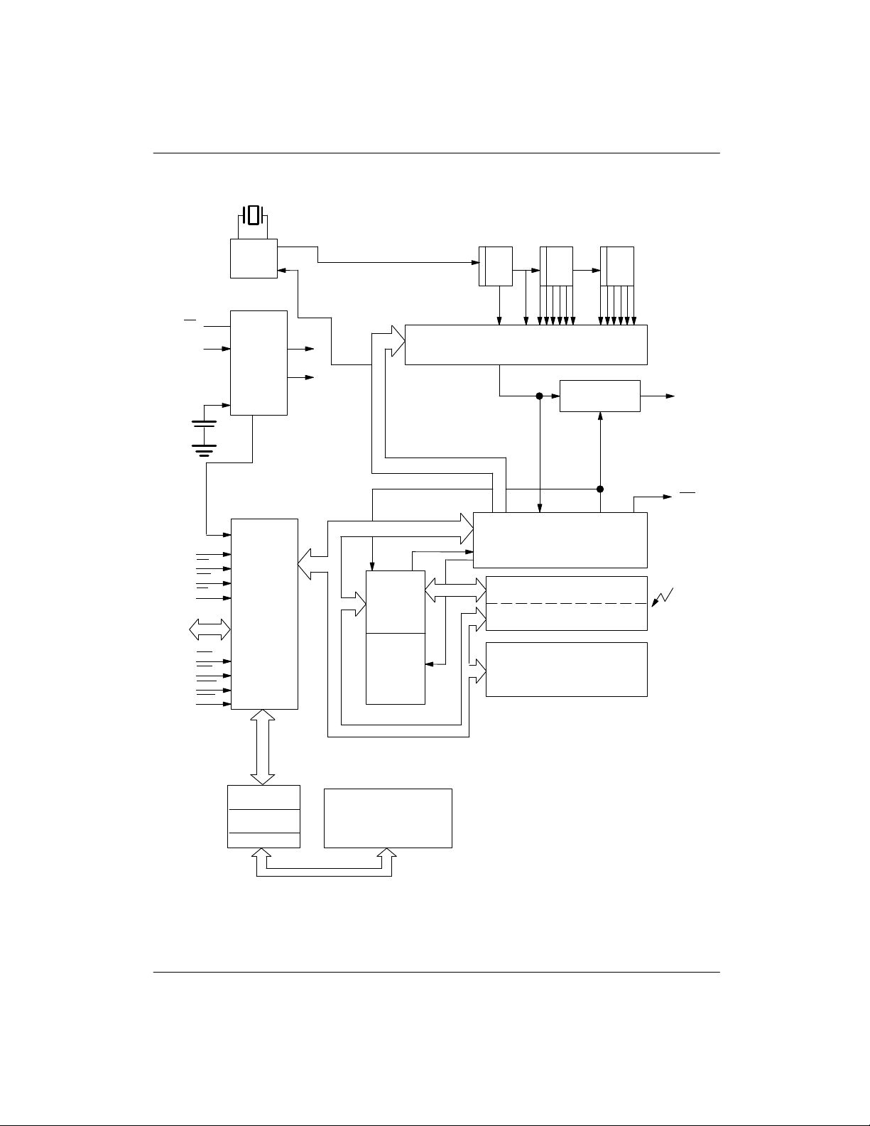
DS1385/DS1387 BLOCK DIAGRAM Figure 1
X1 X2
DS1385/DS1387
+3V
CS
V
V
CC
CC
V
+
–
ALE
RD
WR
CS
AD0-AD7
AS1
AS0
WER
OER
BAT
OSC
POWER
SWITCH
AND
WRITE
PROTECT
BUFFER
ENABLE
BUS
INTERFACE
V
CC
POK
CLOCK/
CALENDAR
UPDATE
BCD/BINARY
INCREMENT
648 64
PERIODIC INTERRUPT/SQUARE WAVE
SELECTOR
CONTROL
REGISTERS A, B, C, D
CLOCK, CALENDAR,
AND ALARM
USER RAM
50 BYTES
SQUARE
WAVE OUT
SQW
IRQ
DOUBLE
BUFFERED
ADDRESS HIGH
BYTE LATCH
ADDRESS LOW
BYTE LATCH
DATA LATCH
NONVOLATILE RAM
4K X 8
012496 3/20
Page 4

DS1385/DS1387
WR (RTC Write Input) –The WR signal is an active low
signal. The WR signal defines the time period during
which data is written to the addressed clock register.
CS
(RTC Chip Select Input) – The Chip Select signal
must be asserted low during a bus cycle for the RTC
portion of the DS1385/DS1387 to be accessed. CS
must be kept in the active state during RD and WR timing. Bus cycles which take place without asserting CS
will latch addresses but no access will occur.
IRQ
(Interrupt Request Output) – The IRQ pin is an
active low output of the DS1385/DS1387 that can be
tied to an interrupt input on a processor. The IRQ
output
remains low as long as the status bit causing the interrupt is present and the corresponding interrupt–enable
bit is set. T o clear the IRQ pin, the application program
normally reads the C register.
When no interrupt conditions are present, the IRQ
level
is in the high impedance state. Multiple interrupting devices can be connected to an IRQ
bus. The IRQ bus is
an open drain output and requires an external pull–up
resistor.
AS0
(RAM Address Strobe Zero) – The rising edge of
AS0 latches the lower eight bits of the 4K x 8 RAM address.
AS1
(RAM Address Strobe One) – The rising edge of
AS1 latches the upper four bits of the 4K x 8 RAM address.
OER
(RAM Output Enable) – OER is active low and
identifies the time period when the DS1385/DS1387
drives the bus with RAM read data.
WER
(RAM Write Enable) – WER is an active low sig-
nal and is used to perform writes to the 4K x 8 RAM portion of the DS1385/DS1387.
nals be kept away from the crystal area. For more
information on crystal selection and crystal layout considerations, please consult Application Note 58, “Crystal Considerations with Dallas Real Time Clocks”.
V
, BGND – Battery input for any standard 3 volt lithi-
BAT
um cell or other energy source. Battery voltage must be
held between 2.5 and 3.7 volts for proper operation. The
nominal write protect trip point voltage is set by the internal circuitry and is 4.25 volts typical. A maximum load of
1 µA at 25°C and 3.0V on V
should in the absence of
BAT
power be used to size the external energy source.
The battery should be connected directly to the V
BAT
pin.
A diode must not be placed in series with the battery to
the V
pin. Furthermore, a diode is not necessary
BAT
because reverse charging current protection circuitry is
provided internal to the device and has passed the
requirements of Underwriters Laboratories for UL listing
(E99151).
ADDRESS MAP
The address map of the DS1385/DS1387 is shown in
Figure 2. The address map consists of the RTC and the
4K X 8 NV SRAM section. The RTC section contains
50–bytes of user RAM, 10–bytes of RAM that contain
the RTC time, calendar, and alarm data, and 4–bytes
which are used for control and status. All 64–bytes can
be directly written or read except for the following:
1. Registers C and D are read-only .
2. Bit–7 of Register A is read-only .
3. The high order bit of the seconds byte is read-only .
RTC (REAL TIME CLOCK)
The RTC function is the same as the DS1287 Real Time
Clock. Access to the RTC is accomplished with four
controls: ALE, RD
the DS1287 with the following exceptions:
, WR and CS. The RTC is the same in
(DS1385 ONL Y)
X1, X2 – Connections for a standard 32.768 KHz quartz
crystal. When ordering, request a load capacitance of 6
pF . The internal oscillator circuitry is designed for operation with a crystal having a specified load capacitance
(CL) of 6 pF . The crystal is connected directly to the X1
and X2 pins. There is no need for external capacitors or
resistors. Note: X1 and X2 are very high impedance
nodes. It is recommended that they and the crystal be
guard–ringed with ground and that high frequency sig-
012496 4/20
1. The MOT pin on the DS1285/DS1287 is not present
on the DS1385/DS1387. The bus selection capability of the DS1285/DS1287 has been eliminated. Only
the Intel bus interface timing is applicable.
2. The RESET
pin on the DS1285/DS1287 is not present on the DS1385/DS1387. The DS1385/DS1387
will operate the same as the DS1285/DS1287 with
tied to VCC.
RESET
Page 5

ADDRESS MAP DS1385/DS1387 Figure 2
DS1385/DS1387
4096
0
13
14
63
0
14–BYTES
50–BYTES
USER RAM
4K X 8
NV SRAM
00
0D
0E
3F
000
FFF
TIME, CALENDAR AND ALARM LOCATIONS
The time and calendar information is obtained by reading the appropriate register bytes shown in T able 1. The
time, calendar and alarm are set or initialized by writing
the appropriate register bytes. The contents of the time,
calendar and alarm registers can be either Binary or
Binary–Coded Decimal (BCD) format. Table 1 shows
the binary and BCD formats of the twelve time, calendar
and alarm locations.
Before writing the internal time, calendar and alarm registers, the SET bit in Register B should be written to a
logic one to prevent updates from occurring while access is being attempted. Also at this time, the data format (binary or BCD), should be set via the data mode bit
(DM) of Register B. All time, calendar and alarm registers must use the same data mode. The set bit in Register B should be cleared after the data mode bit has been
written to allow the real–time clock to update the time
and calendar bytes.
Once initialized, the real–time clock makes all updates
in the selected mode. The data mode cannot be
changed without reinitializing the ten data bytes. The
24/12 bit cannot be changed without reinitializing the
hour locations. When the 12–hour format is selected,
0
1
2
3
4
5
6
7
8
9
10
11
12
13
SECONDS
SECONDS ALARM
MINUTES
MINUTES ALARM
HOURS
HOURS ALARM
DAY OF THE WEEK
DAY OF THE MONTH
MONTH
YEAR
REGISTER A
REGISTER B
REGISTER C
REGISTER D
the high order bit of the hours byte represents PM when
it is a logic one. The time, calendar and alarm bytes are
always accessible because they are double buffered.
Once per second the 10–bytes are advanced by one
second and checked for an alarm condition. If a read of
the time and calendar data occurs during an update, a
problem exists where seconds, minutes, hours, etc.
may not correlate. The probability of reading incorrect
time and calendar data is low. Several methods of
avoiding any possible incorrect time and calendar reads
are covered later in this text.
The three alarm bytes can be used in two ways. First,
when the alarm time is written in the appropriate hours,
minutes and seconds alarm locations, the alarm interrupt is initiated at the specified time each day if the alarm
enable bit is high. The second method is to insert a
“don’t care” state in one or more of the three alarm bytes.
The “don’t care” code is any hexadecimal value from C0
to FF . The two most significant bits of each byte set the
“don’t care” condition when at logic 1. An alarm will be
generated each hour when the “don’t care” bits are set in
the hours byte. Similarly, an alarm is generated every
minute with “don’t care” codes in the hours and minute
alarm bytes. The “don’t care” codes in all three alarm
bytes create an interrupt every second.
BINARY OR BCD INPUTS
012496 5/20
Page 6

DS1385/DS1387
ADDRESS
FUNCTION
DECIMAL
TIME, CALENDAR AND ALARM DATA MODES Table 1
ADDRESS
LOCATION
0 Seconds 0–59 00–3B 00–59
1 Seconds Alarm 0–59 00–3B 00–59
2 Minutes 0–59 00–3B 00–59
3 Minutes Alarm 0–59 00–3B 00–59
4 Hours–12–hr Mode 1–12 01–0C AM, 81–8C PM 01–12AM, 81–92PM
Hours–24–hr Mode 0–23 00–17 00–23
5 Hours Alarm–12–hr 1–12 01–0C AM, 81–8C PM 01–12AM, 81–92PM
Hours Alarm–24–hr 0–23 00–17 00–23
6 Day of the Week
Sunday = 1
7 Date of the Month 1–31 01–1F 01–31
8 Month 1–12 01–0C 01–12
9 Y ear 0–99 00–63 00–99
DECIMAL
RANGE
BINARY DATA MODE BCD DATA MODE
1–7 01–07 01–07
RANGE
USER NONVOLATILE RAM – RTC
The 50 user nonvolatile RAM bytes are not dedicated to
any special function within the DS1385/DS1387. They
can be used by the application program as nonvolatile
memory and are fully available during the update cycle.
This memory is directly accessible in the RTC section.
INTERRUPTS
The RTC plus RAM includes three separate, fully automatic sources of interrupt for a processor. The alarm interrupt can be programmed to occur at rates from once
per second to once per day. The periodic interrupt can
be selected for rates from 500 ms to 122 µs. The
update–ended interrupt can be used to indicate to the
program that an update cycle is complete. Each of
these independent interrupt conditions is described in
greater detail in other sections of this text.
The application program can select which interrupts, if
any, are going to be used. Three bits in Register B enable the interrupts. Writing a logic 1 to an interrupt–enable bit permits that interrupt to be initiated when the
event occurs. A logic 0 in an interrupt–enable bit prohibits the IRQ pin from being asserted from that interrupt
condition. If an interrupt flag is already set when an interrupt is enabled, IRQ
is immediately set at an active
level, although the interrupt initiating the event may
have occurred much earlier. As a result, there are cases
where the program should clear such earlier initiated interrupts before first enabling new interrupts.
When an interrupt event occurs, the relating flag bit is
set to logic 1 in Register C. These flag bits are set independent of the state of the corresponding enable bit in
Register B. The flag bit can be used in a polling mode
without enabling the corresponding enable bits. When a
flag is set, an indication is given to software that an interrupt event has occurred since the flag bit was last read.
However, care should be taken when using the flag bits
as they are cleared each time Register C is read.
Double latching is included with Register C so that bits
which are set remain stable throughout the read cycle.
All bits which are set (high) are cleared when read and
new interrupts which are pending during the read cycle
are held until after the cycle is completed. One, two or
three bits can be set when reading Register C. Each utilized flag bit should be examined when read to ensure
that no interrupts are lost.
012496 6/20
Page 7

DS1385/DS1387
tPI PERIODIC
SQW OUTPUT
The alternative flag bit usage method is with fully enabled interrupts. When an interrupt flag bit is set and the
corresponding interrupt enable bit is also set, the IRQ
pin is asserted low. IRQ is asserted as long as at least
one of the three interrupt sources has its flag and enable
will turn the oscillator on and enable the countdown
chain. A pattern of 11X will turn the oscillator on, but
holds the countdown chain of the oscillator in reset. All
other combinations of bits 6 through 4 keep the oscilla-
tor off.
bits both set. The IRQF bit in Register C is a one whenever the IRQ
the RTC initiated an interrupt is accomplished by reading Register C. A logic one in bit–7 (IRQF bit) indicates
that one or more interrupts have been initiated. The act
of reading Register C clears all active flag bits and the
IRQF bit.
pin is being driven low. Determination that
SQUARE WAVE OUTPUT SELECTION
Thirteen of the 15 divider taps are made available to a
1–of–15 selector, as shown in the block diagram of Fig-
ure 1. The first purpose of selecting a divider tap is to
generate a square wave output signal on the SQW pin.
The RS3–RS0 bits in Register A establish the square
wave output frequency . These frequencies are listed in
OSCILLATOR CONTROL BITS
When the DS1385/DS1387 is shipped from the factory ,
the internal oscillator is turned off. This feature prevents
the lithium battery from being used until it is installed in a
system. A pattern of 010 in bits 6 through 4 of Register A
Table 2. The SQW frequency selection shares its
1–of–15 selector with the periodic interrupt generator.
Once the frequency is selected, the output of the SQW
pin can be turned on and off under program control with
the square wave enable bit (SQWE).
PERIODIC INTERRUPT RATE AND SQUARE WAVE OUTPUT FREQUENCY Table 2
SELECT BITS REGISTER A
RS3 RS2 RS1 RS0
0 0 0 0 None None
0 0 0 1 3.90625 ms 256 Hz
0 0 1 0 7.8125 ms 128 Hz
0 0 1 1 122.070 µs 8.192 KHz
0 1 0 0 244.141 µs 4.096 KHz
0 1 0 1 488.281 µs 2.048 KHz
0 1 1 0 976.5625 µs 1.024 KHz
0 1 1 1 1.953125 ms 512 Hz
1 0 0 0 3.90625 ms 256 Hz
1 0 0 1 7.8125 ms 128 Hz
1 0 1 0 15.625 ms 64 Hz
1 0 1 1 31.25 ms 32 Hz
1 1 0 0 62.5 ms 16 Hz
1 1 0 1 125 ms 8 Hz
1 1 1 0 250 ms 4 Hz
1 1 1 1 500 ms 2 Hz
tPI PERIODIC SQW OUTPUT
INTERRUPT RATE
FREQUENCY
012496 7/20
Page 8
DS1385/DS1387
PERIODIC INTERRUPT SELECTION
The periodic interrupt will cause the IRQ pin to go to an
active state from once every 500 ms to once every
122 µs. This function is separate from the alarm inter-
rupt which can be output from once per second to once
per day. The periodic interrupt rate is selected using the
same Register A bits which select the square wave frequency (see T able 1). Changing the Register A bits affects both the square wave frequency and the periodic
interrupt output. However, each function has a separate
enable bit in Register B. The SQWE bit controls the
square wave output. Similarly, the periodic interrupt is
enabled by the PIE bit in Register B. The periodic interrupt can be used with software counters to measure inputs, create output intervals or await the next needed
software function.
UPDATE CYCLE
The DS1385/DS1387 executes an update cycle once
per second regardless of the SET bit in Register B.
When the SET bit in Register B is set to one, the user
copy of the double buffered time, calendar and alarm bytes is frozen and will not update as the time increments.
However, the time countdown chain continues to update
the internal copy of the buffer . This feature allows time to
maintain accuracy independent of reading or writing the
time, calendar and alarm buffers and also guarantees
that time and calendar information is consistent. The update cycle also compares each alarm byte with the corresponding time byte and issues an alarm if a match or if
a “don’t care” code is present in all three positions.
There are three methods that can handle access of the
real–time clock that avoid any possibility of accessing
inconsistent time and calendar data. The first method
uses the update–ended interrupt. If enabled, an interrupt occurs after every up date cycle that indicates that
over 999 ms are available to read valid time and date information. If this interrupt is used, the IRQF bit in Register C should be cleared before leaving the interrupt routine.
A second method uses the update–in–progress bit
(UIP) in Register A to determine if the update cycle is in
progress. The UIP bit will pulse once per second. After
the UIP bit goes high, the update transfer occurs 244 µs
later. If a low is read on the UIP bit, the user has at least
244 µs before the time/calendar data will be changed.
Therefore, the user should avoid interrupt service routines that would cause the time needed to read valid
time/calendar data to exceed 244 µs.
The third method uses a periodic interrupt to determine
if an update cycle is in progress. The UIP bit in Register
A is set high between the setting of the PF bit in Register
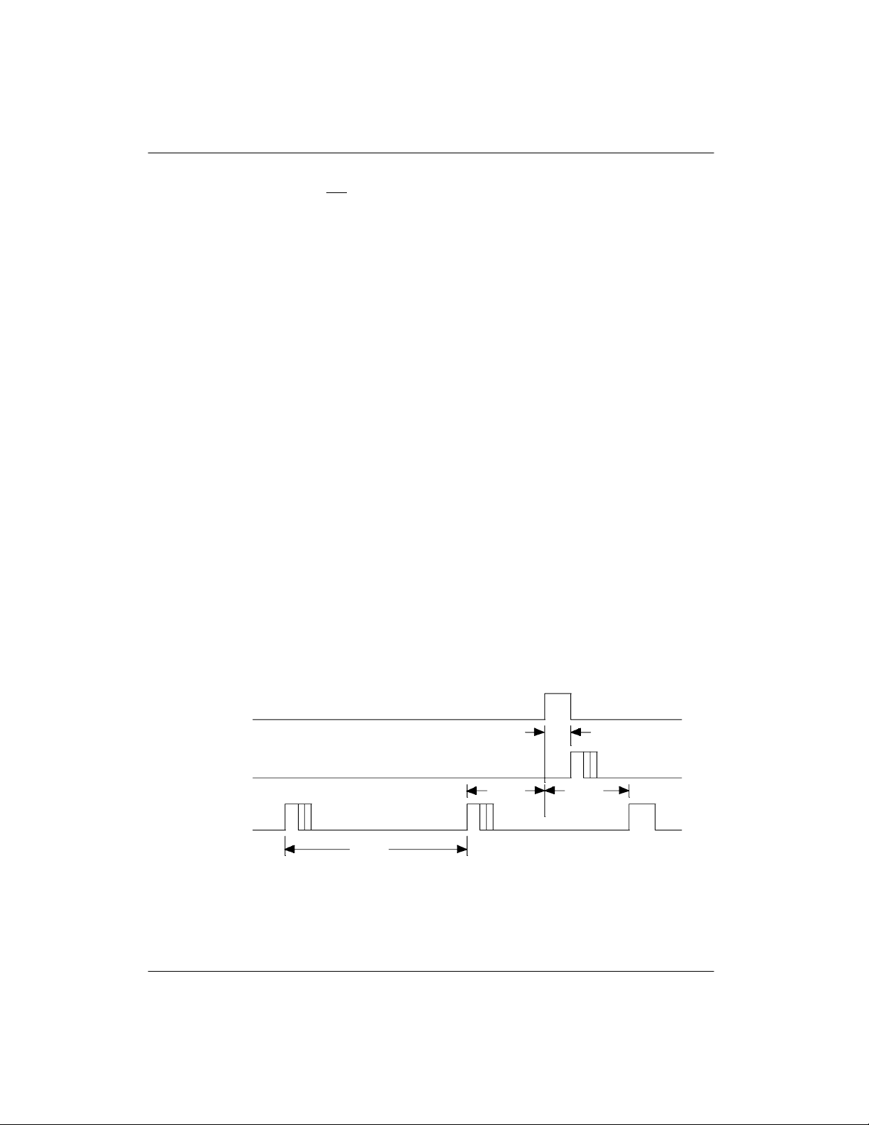
C (see Figure 3). Periodic interrupts that occur at a rate
of greater than t
allow valid time and date informa-
BUC
tion to be reached at each occurrence of the periodic interrupt. The reads should be complete within
(tPI/2+t
) to ensure that data is not read during the up-
BUC
date cycle.
UPDATE–ENDED AND PERIODIC INTERRUPT RELATIONSHIP Figure 3
UIP BIT IN
REGISTER A
UF BIT IN
REGISTER C
PF BIT IN
REGISTER C
012496 8/20
= Periodic interrupt time interval per Table 1.
t
PI
t
= Delay time before update cycle = 244 µs.
BUC
t
PI
t
BUC
t
PI/2
t
PI/2
Page 9
DS1385/DS1387
REGISTERS
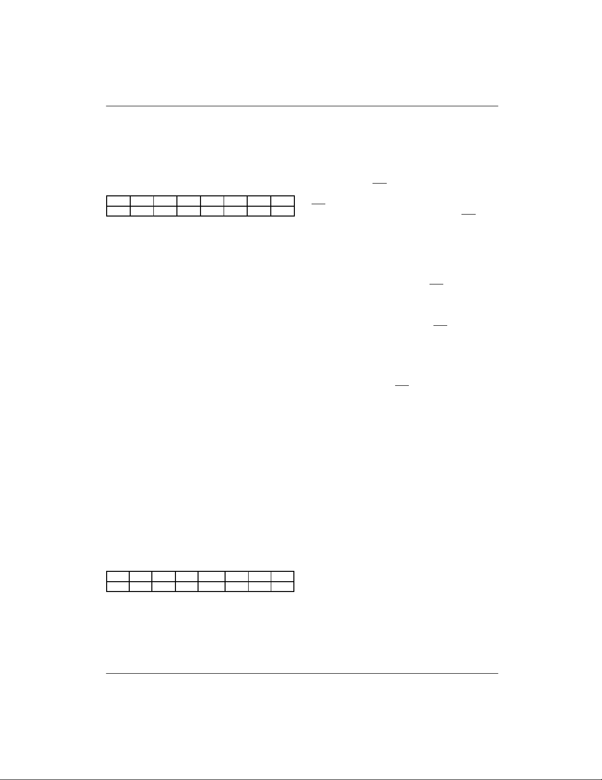
The DS1385/DS1387 has four control registers which
are accessible at all times, even during the update
cycle.
REGISTER A
MSB LSB
BIT 7 BIT 6 BIT 5 BIT 4 BIT 3 BIT 2 BIT 1 BIT 0
UIP DV2 DV1 DV0 RS3 RS2 RS1 RS0
UIP – The Update In Progress (UIP) bit is a status flag
that can be monitored. When the UIP bit is a one, the
update transfer will soon occur. When UIP is a zero, the
update transfer will not occur for at least 244 µs. The
time, calendar and alarm information in RAM is fully
available for access when the UIP bit is zero. The UIP
bit is read only. W riting the SET bit in Register B to a one
inhibits any update transfer and clears the UIP status
bit.
DV2, DV1, DV0 – These three bits are used to turn the
oscillator on or off and to reset the countdown chain. A
pattern of 010 is the only combination of bits that will turn
the oscillator on and allow the RTC to keep time. A pattern of 11X will enable the oscillator but holds the countdown chain in reset. The next update will occur at 500
ms after a pattern of 010 is written to DV2, DV1, and
DV0.
the midst of initializing. Read cycles can be executed in
a similar manner. SET is a read/write bit that is not modi-
fied by internal functions of the DS1385/DS1387.
PIE – The Periodic Interrupt Enable bit is a read/write bit
which allows the Periodic Interrupt Flag (PF) bit in Reg-
ister C to drive the IRQ
pin low. When the PIE bit is set to
one, periodic interrupts are generated by driving the
pin low at a rate specified by the RS3-RS0 bits of
IRQ
Register A. A zero in the PIE bit blocks the IRQ
output
from being driven by a periodic interrupt, but the Periodic Flag (PF) bit is still set at the periodic rate. PIE is not
modified by any internal DS1385/DS1387 functions.
AIE – The Alarm Interrupt Enable (AIE) bit is a read/
write bit which, when set to a one, permits the Alarm
Flag (AF) bit in register C to assert IRQ. An alarm interrupt occurs for each second that the three time bytes
equal the three alarm bytes including a don’t care alarm
code of binary 11XXXXXX. When the AIE bit is set to
zero, the AF bit does not initiate the IRQ
signal. The internal functions of the DS1385/DS1387 do not affect the
AIE bit.
UIE – The Update Ended Interrupt Enable (UIE) bit is a
read/write bit that enables the Update End Flag (UF) bit
in Register C to assert IRQ. The SET bit going high
clears the UIE bit.
RS3, RS2, RS1, RS0 – These four rate–selection bits
select one of the 13 taps on the 15–stage divider or disable the divider output. The tap selected can be used to
generate an output square wave (SQW pin) and/or a periodic interrupt. The user can do one of the following:
1. Enable the interrupt with the PIE bit;
2. Enable the SQW output pin with the SQWE bit;
3. Enable both at the same time and the same rate; or
4. Enable neither.
Table 2 lists the periodic interrupt rates and the square
wave frequencies that can be chosen with the RS bits.
REGISTER B
MSB LSB
BIT 7 BIT 6 BIT 5 BIT 4 BIT 3 BIT 2 BIT 1 BIT 0
SET PIE AIE UIE SQWE DM 24/12 DSE
SET – When the SET bit is a zero, the update transfer
functions normally by advancing the counts once per
second. When the SET bit is written to a one, any update
transfer is inhibited and the program can initialize the
time and calendar bytes without an update occurring in
SQWE – When the Square Wave Enable (SQWE) bit is
set to a one, a square wave signal at the frequency set
by the rate–selection bits RS3 through RS0 is driven out
on a SQW pin. When the SQWE bit is set to zero, the
SQW pin is held low. SQWE is a read/write bit.
DM – The Data Mode (DM) bit indicates whether time
and calendar information is in binary or BCD format.
The DM bit is set by the program to the appropriate format and can be read as required. This bit is not modified
by internal functions. A one in DM signifies binary data
while a zero in DM specifies Binary Coded Decimal
(BCD) data.
24/12 – The 24/12 control bit establishes the format of
the hours byte. A one indicates the 24–hour mode and a
zero indicates the 12–hour mode. This bit is read/write.
DSE – The Daylight Savings Enable (DSE) bit is a read/
write bit which enables two special updates when DSE
is set to one. On the first Sunday in April the time increments from 1:59:59 AM to 3:00:00 AM. On the last
Sunday in October when the time first reaches 1:59:59
012496 9/20
Page 10

DS1385/DS1387
AM it changes to 1:00:00 AM. These special updates do
not occur when the DSE bit is a zero. This bit is not affected by internal functions.
REGISTER C
MSB LSB
BIT 7 BIT 6 BIT 5 BIT 4 BIT 3 BIT 2 BIT 1 BIT 0
IRQF PF AF UF 0 0 0 0
IRQF - The Interrupt Request Flag (IRQF) bit is set to a
one when one or more of the following are true:
PF = PIE = 1
AF = AIE = 1
UF = UIE = 1
i.e., IRQF =
(PF • PIE) + (AF • AIE) + (UF • UIE)
Any time the IRQF bit is a one, the IRQ pin is driven low.
All flag bits are cleared after Register C is read by the
program.
PF – The Periodic Interrupt Flag (PF) is a read–only bit
which is set to a one when an edge is detected on the
selected tap of the divider chain. The RS3 through RS0
bits establish the periodic rate. PF is set to a one independent of the state of the PIE bit. When both PF and
PIE are ones, the IRQ
signal is active and will set the
IRQF bit. The PF bit is cleared by a software read of
Register C.
AF – A one in the Alarm Interrupt Flag (AF) bit indicates
that the current time has matched the alarm time. If the
AIE bit is also a one, the IRQ
pin will go low and a one will
appear in the IRQF bit. A read of Register C will clear
AF.
UF – The Update Ended Interrupt Flag (UF) bit is set after each update cycle. When the UIE bit is set to one, the
one in UF causes the IRQF bit to be a one which will assert the IRQ
pin. UF is cleared by reading Register C.
BIT 3 THROUGH BIT 0 – These are reserved bits of the
status Register C. These bits always read zero and cannot be written.
REGISTER D
MSB LSB
BIT 7 BIT 6 BIT 5 BIT 4 BIT 3 BIT 2 BIT 1 BIT 0
VRT 0 0 0 0 0 0 0
VRT – The Valid RAM and Time (VRT) bit is set to the
one state by Dallas Semiconductor Corporation prior to
shipment. This bit is not writable and should always be a
one when read. If a zero is ever present, an exhausted
internal lithium energy source is indicated and both the
contents of the RTC data and RAM data are questionable.
BIT 6 THROUGH BIT 0 – The remaining bits of Register
D are reserved and not usable. They cannot be written
and, when read, they will always read zero.
4K X 8 RAM
The DS1385/DS1387 provides 4K x 8 of on–chip SRAM
which is controlled as nonvolatile storage sustained
from a lithium battery. On power–up, the RAM is taken
out of write–protect status by the internal power OK signal (POK) generated from the write protect circuitry.
The POK signal becomes active at 4.25 volts (typical).
The on–chip 4K x 8 nonvolatile SRAM is accessed via
the eight multiplexed address/data lines AD7–AD0. Access to the SRAM is controlled by three on–chip latch
registers. Two registers are used to hold the SRAM address and the third register is used to hold read/write
data. The SRAM address space is from 000H to FFFH.
Four control signals, AS0
used to access the 4K x 8 SRAM. The address latches
are loaded from the address/data bus in response to rising edge signals applied to the Address Strobe 0 (AS0
and Address Strobe 1 (AS1
latch the lower 8–bits of address, and AS1
latch the upper 4–bits of address. It is necessary to
meet the setup and hold times given in the Electrical
Specifications with valid address information in order to
properly latch the address. If the upper or lower order
address is correct from a prior cycle, it is not necessary
to repeat the address latching sequence.
A write operation requires valid data to be placed on the
bus (AD7–AD0) followed by the activation of the Write
Enable RAM (WER
to the RAM provided that the write timing specifications
are met. During a read cycle, the Output Enable RAM
) signal is driven active. Data from the RAM will
(OER
become valid on the bus provided that the RAM read access timing specifications are met. The WER and OER
signals should never be active at the same time. In addition, access to the clock/calendar registers and user
RAM (via CS
) must not be attempted when the 4K x 8
RAM is being accessed. The RAM is enabled when either WER or OER is active. CS is only used for the access of the clock calendar registers (including the extended Dallas registers) and the 50–bytes of user RAM.
, AS1, OER, and WER, are
) signals. AS0 is used to
is used to
) line. Data on the bus will be written
)
012496 10/20
Page 11

DS1385/DS1387
ABSOLUTE MAXIMUM RATINGS*
Voltage on any Pin Relative to Ground –0.3V to +7.0V
Operating Temperature 0°C to 70°C
Storage Temperature DS1387: –40°C to +70°C
DS1385: –55°C to +125°C
Soldering Temperature 260
°C for 10 seconds
* This is a stress rating only and functional operation of the device at these or any other conditions above those
indicated in the operation sections of this specification is not implied. Exposure to absolute maximum rating
conditions for extended periods of time may affect reliability.
RECOMMENDED DC OPERATING CONDITIONS (0°C to 70°C)
PARAMETER SYMBOL MIN TYP MAX UNITS NOTES
Power Supply Voltage V
Input Logic 1 V
Input Logic 0 V
Battery Voltage V
CC
IH
IL
BAT
4.5 5.0 5.5 V 1
2.2 VCC+0.3 V 1
–0.3 +0.8 V 1
2.5 3.7 V 9
DC ELECTRICAL CHARACTERISTICS (0°C to 70°C)
PARAMETER SYMBOL MIN TYP MAX UNITS NOTES
Power Supply Current I
Standby Current CS, OER and
WER
= VCC –0.3 volt
Input Leakage I
I/O Leakage I
Output @ 2.4 volts I
Output @ 0.4 volts I
CC1
I
CC2
IL
LO
OH
OL
–1.0 +1.0 µA 3
–1.0 +1.0 µA 3
–1.0 mA 1, 4
35 50 mA 2
1 5.0 mA 6
2.0 mA 1
012496 11/20
Page 12

DS1385/DS1387
RTC AC TIMING CHARACTERISTICS (0°C to 70°C; VCC = 4.5V to 5.5V)
PARAMETER SYMBOL MIN TYP MAX UNITS NOTES
Cycle Time t
CYC
Pulse Width, RD/WR Low PW
Pulse Width, RD/WR High PW
Input Rise and Fall Time tR, t
Chip Select Setup Time Before
or RD
WR
Chip Select Hold Time t
Read Data Hold Time t
Write Data Hold Time t
Muxed Address Valid Time to
ALE Fall
Muxed Address Hold Time from
ALE Fall
RD or WR High Setup to ALE
Rise
t
CS
CH
DHR
DHW
t
ASL
t
AHL
t
ASD
Pulse Width ALE High PW
ALE Low Setup to RD or WR Fall t
Output Data Delay Time from RD t
Data Setup Time to Write t
IRQ Release from RD t
ASED
DDR
DSW
IRD
EH
EL
F
ASH
305 DC ns
125 ns
150 ns
30 ns
20 ns
0 ns
10 80 ns
0 ns
30 ns
10 ns
25 ns
60 ns
40 ns
20 120 ns 5
100 ns
2 µs
012496 12/20
Page 13
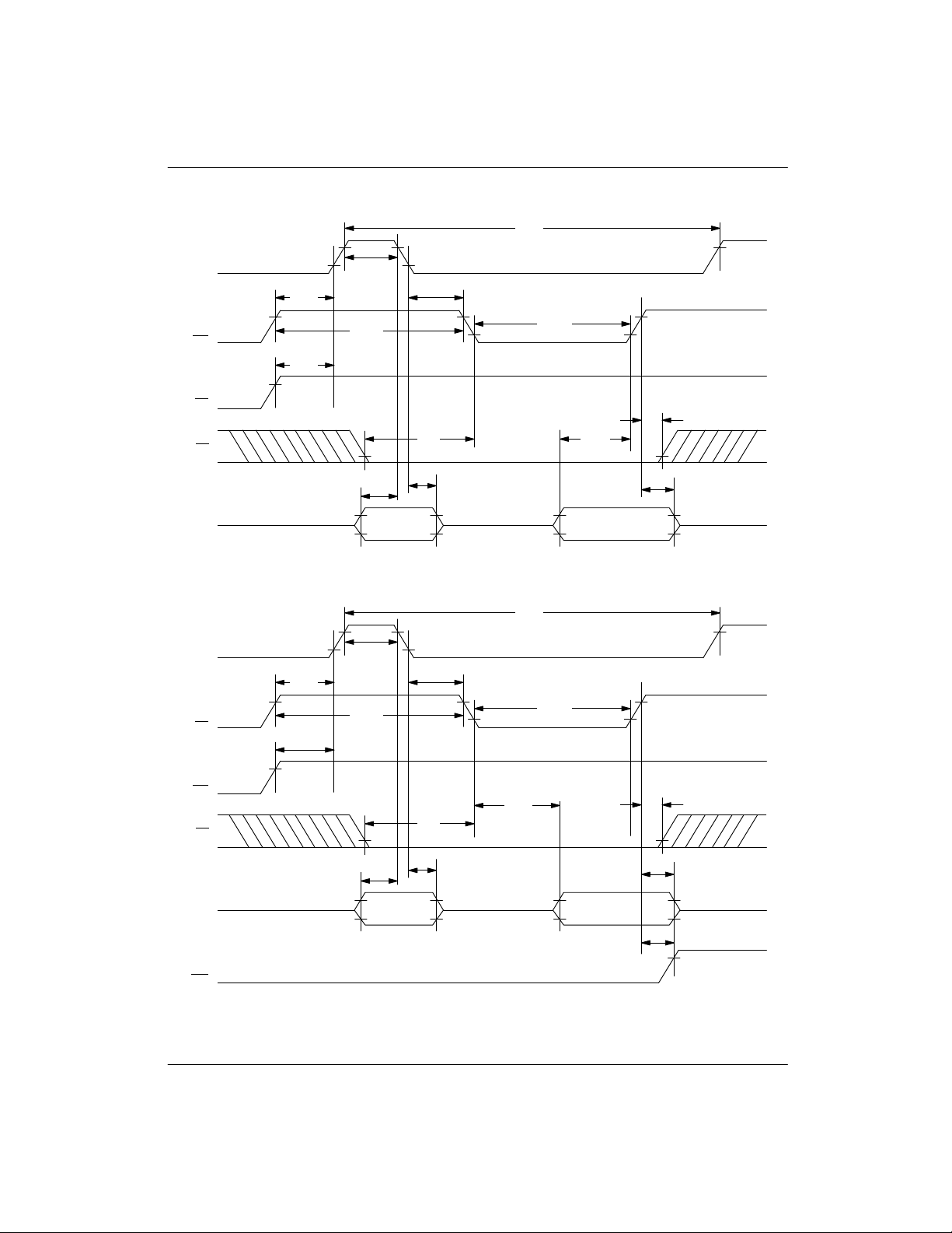
DS1385/DS1387 BUS TIMING FOR WRITE CYCLE TO RTC
t
CYC
PW
ASH
ALE
t
ASED
WR
t
t
ASD
ASD
PW
EL
PW
DS1385/DS1387
EH
RD
t
CS
t
ASL
CS
t
AHL
AD0–AD7
DS1385/DS1387 BUS TIMING FOR READ CYCLE TO RTC
t
CYC
PW
ASH
ALE
t
ASED
t
t
CS
t
AHL
DDR
WR
RD
CS
t
t
ASD
ASD
PW
EL
t
ASL
PW
t
CH
t
DSW
t
DHW
EH
t
CH
t
DHR
AD0–AD7
IRQ
t
IRD
012496 13/20
Page 14
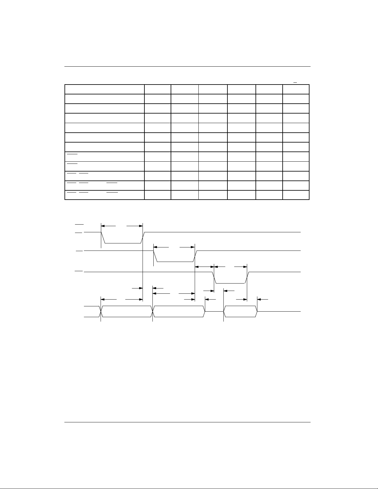
DS1385/DS1387
4K X 8 AC TIMING CHARACTERISTICS (0°C to 70°C; VCC = 5V + 10%)
PARAMETER SYMBOL MIN TYP MAX UNITS NOTES
Address Setup Time t
Address Hold Time t
Data Setup Time t
Data Hold Time t
Output Enable Access Time t
Write Pulse Width t
OER Pulse Width t
OER to Output in High Z t
AS0, AS1 Pulse Width t
AS0, AS1 High to OER Low t
AS0, AS1 High to WER Low t
AS
AH
DS
DH
OEA
WP
RP
OEZ
ASP
ASO
ASW
55 ns
0 ns
75 ns
0 ns
200 ns 7
200 ns
200 ns
50 ns
75 ns
20 ns
20 ns
BUS TIMING FOR READ CYCLE TO 4K X 8 NV SRAM
t
WER = V
AS0
IH
ASP
AS1
OER
AD0–AD7
t
ASP
t
AH
t
AS
LOW ADDRESS VALID UPPER ADDRESS VALID
t
AS
t
ASO
t
AH
t
OEA
t
RP
DATA OUT
VALID
t
OEZ
012496 14/20
Page 15
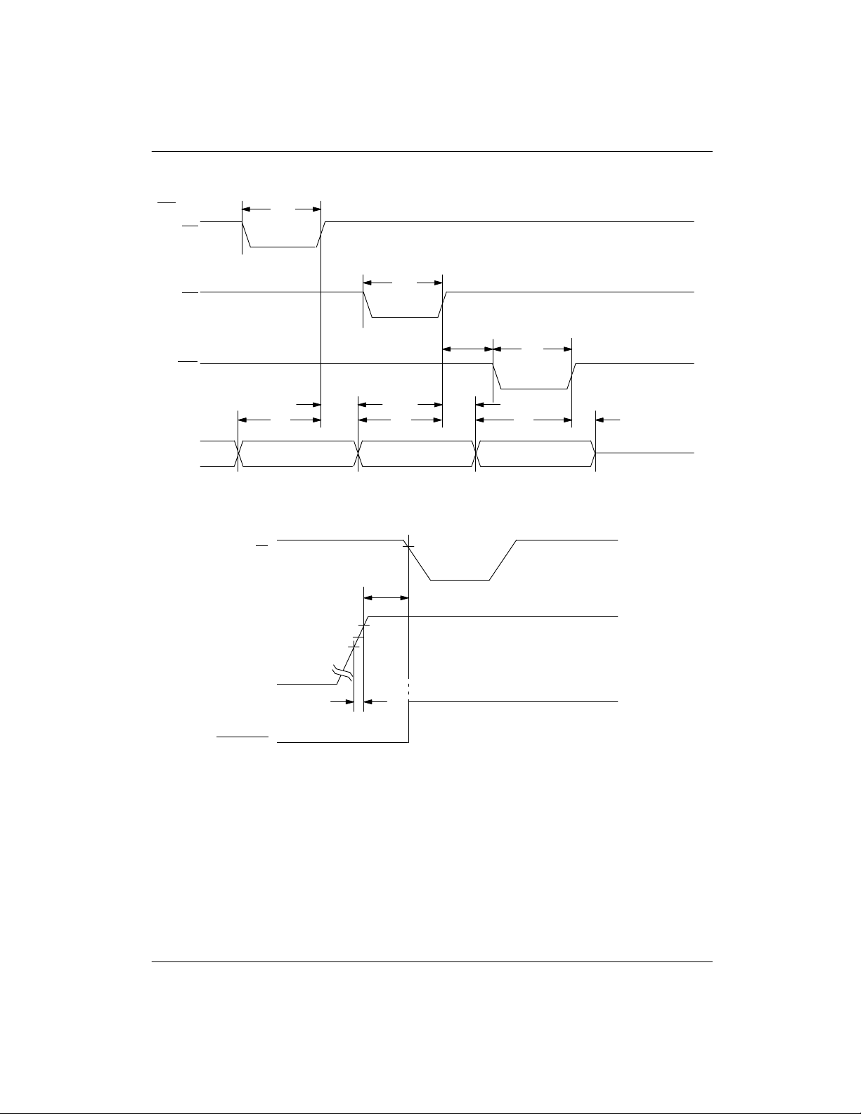
BUS TIMING FOR WRITE CYCLE TO 4K X 8 SRAM
OER
= V
AS0
AS1
WER
IH
t
ASP
t
ASP
t
ASW
DS1385/DS1387
t
WP
t
AS
AD0–AD7
LOW ADDRESS VALID
POWER–UP CONDITION
CE
V
CC
POWER FAIL
t
AH
UPPER ADDRESS VALID
4.5V
4.25V
4.0V
t
REC
t
t
AS
AH
t
DS
t
DH
DATA IN VALID
V
IH
t
R
012496 15/20
Page 16
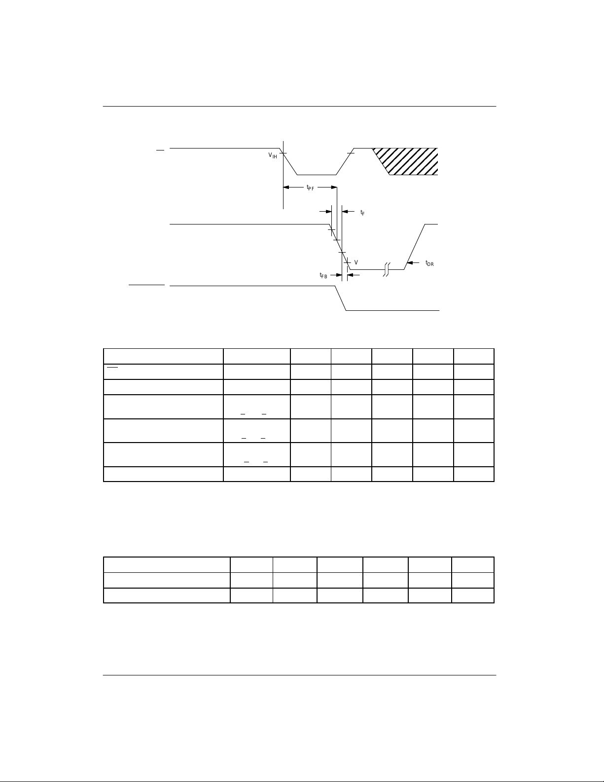
DS1385/DS1387
POWER–DOWN CONDITION
CE
V
POWER FAIL
CC
V
IH
t
PF
t
F
4.5V
4.25V
4.0V
V
BAT
t
FB
t
DR
POWER–UP POWER–DOWN TIMING (tA = 25°C)
PARAMETER SYMBOL MIN TYP MAX UNITS NOTES
CE High to Power Fail t
Recovery at Power Up t
VCC Slew Rate Power Down t
4.0 <VCC < 4.5V
VCC Slew Rate Power Down t
3.0 <VCC< 4.0V
VCC Slew Rate Power Up t
4.5V>VCC>4.0V
Expected Data Retention t
PF
REC
F
FB
R
DR
150 ms
300 µs
10 µs
0 µs
10 years 8
0 ns
WARNING:
Under no circumstances are negative undershoots, of any amplitude, allowed when device is in battery back–up
mode.
CAPACITANCE (tA = 25°C)
PARAMETER SYMBOL MIN TYP MAX UNITS NOTES
Input Capacitance C
Output Capacitance C
012496 16/20
IN
OUT
12 pF
12 pF
Page 17
DS1385/DS1387
NOTES:
1. All voltages are referenced to ground.
2. All outputs are open.
3. Applies to the AD0–AD7 pins and the SQW pin when each is in the high impedance state.
4. The IRQ
pin is open drain.
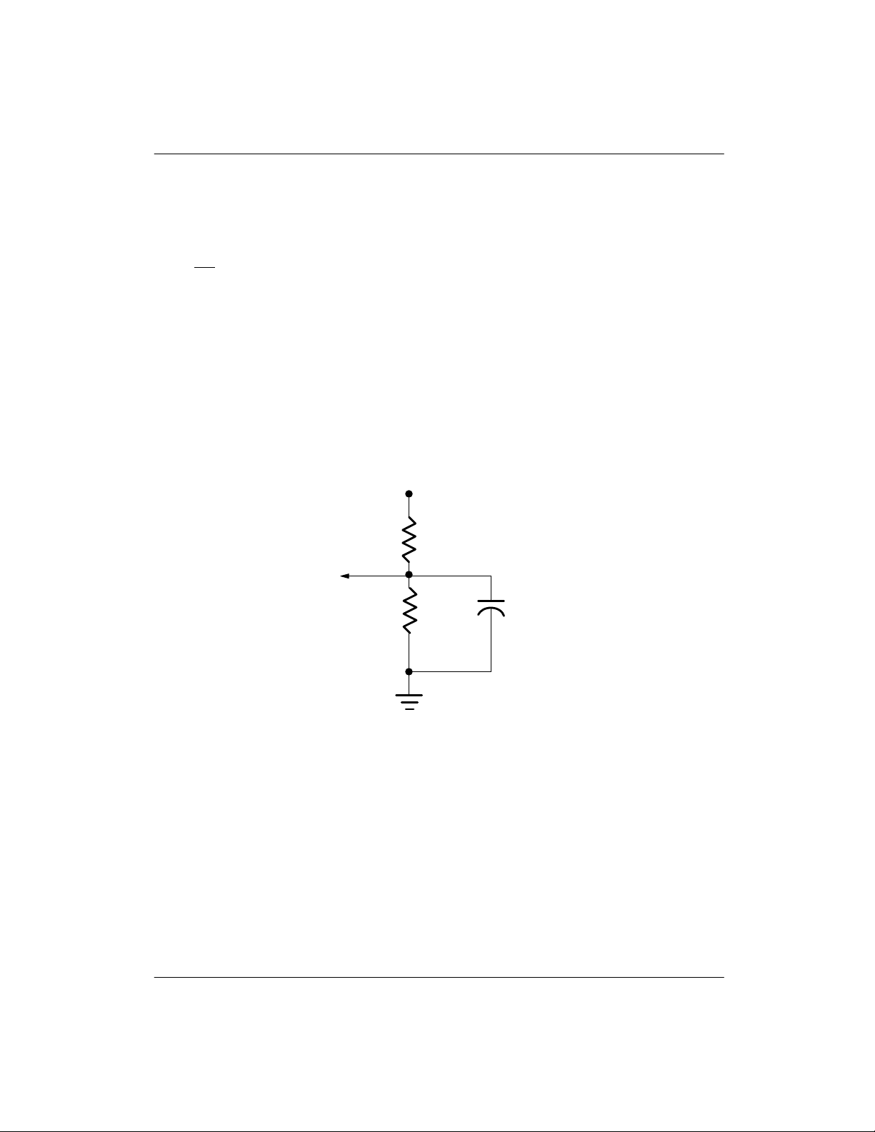
5. Measured with a load as shown in Figure 4.
6. All other inputs at CMOS levels.
7. Measured with a load as shown in Figure 4.
8. The real–time clock will keep time to an accuracy of ±1 minute per month during data retention time for the
period of t
DR
.
9. Applies to DS1385 and DS1385S only .
OUTPUT LOAD Figure 4
+5 VOLTS
1.1KΩ
D.U.T.
680
50 pF
012496 17/20
Page 18
DS1385/DS1387
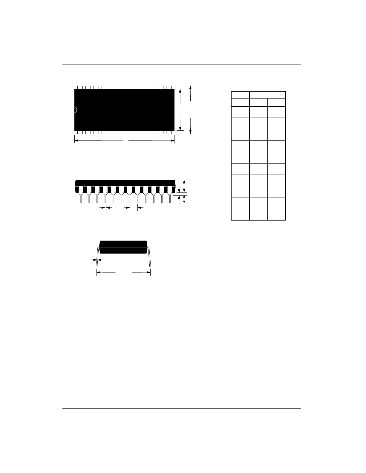
DS1385 24–PIN DIP
1
K
24–PINPKG
DIM MIN MAX
B D
A
C
F
G
E
A IN.
MM
B IN.
MM
C IN.
MM
D IN.
MM
E IN.
MM
F IN.
MM
G IN.
MM
H IN.
MM
J IN.
MM
K IN.
MM
1.245
31.62
0.530
13.46
0.140
3.56
0.600
15.24
0.015
0.38
0.120
3.05
0.090
2.29
0.625
15.88
0.008
0.20
0.015
0.38
1.270
32.26
0.550
13.97
0.160
4.06
0.625
15.88
0.050
1.27
0.145
3.68
0.110
2.79
0.675
17.15
0.012
0.30
0.022
0.56
012496 18/20
J
H
Page 19
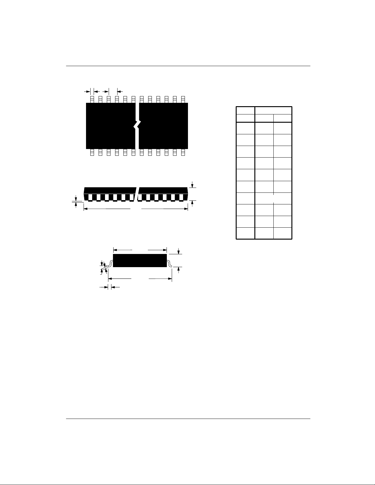
DS1385S 28–PIN SOIC
K G
E
DS1385/DS1387
28–PINPKG
DIM MIN MAX
A IN.
0.706
MM
17.93
B IN.
0.338
MM
8.58
C IN.
D IN.
C
A
G IN.
H IN.
MM
MM
E IN.
MM
F IN.
MM
MM
MM
J IN.
MM
K IN.
MM
0.086
2.18
0.020
0.58
0.002
0.05
0.090
2.29
0.050 BSC
1.27
0.460
11.68
0.006
0.15
0.014
0.36
0.728
18.49
0.350
8.89
0.110
2.79
0.050
1.27
0.014
0.36
0.124
3.15
0.480
12.19
0.013
0.33
0.020
0.51
0–8 deg. typ.
B
F
J
H
D
012496 19/20
Page 20
DS1385/DS1387
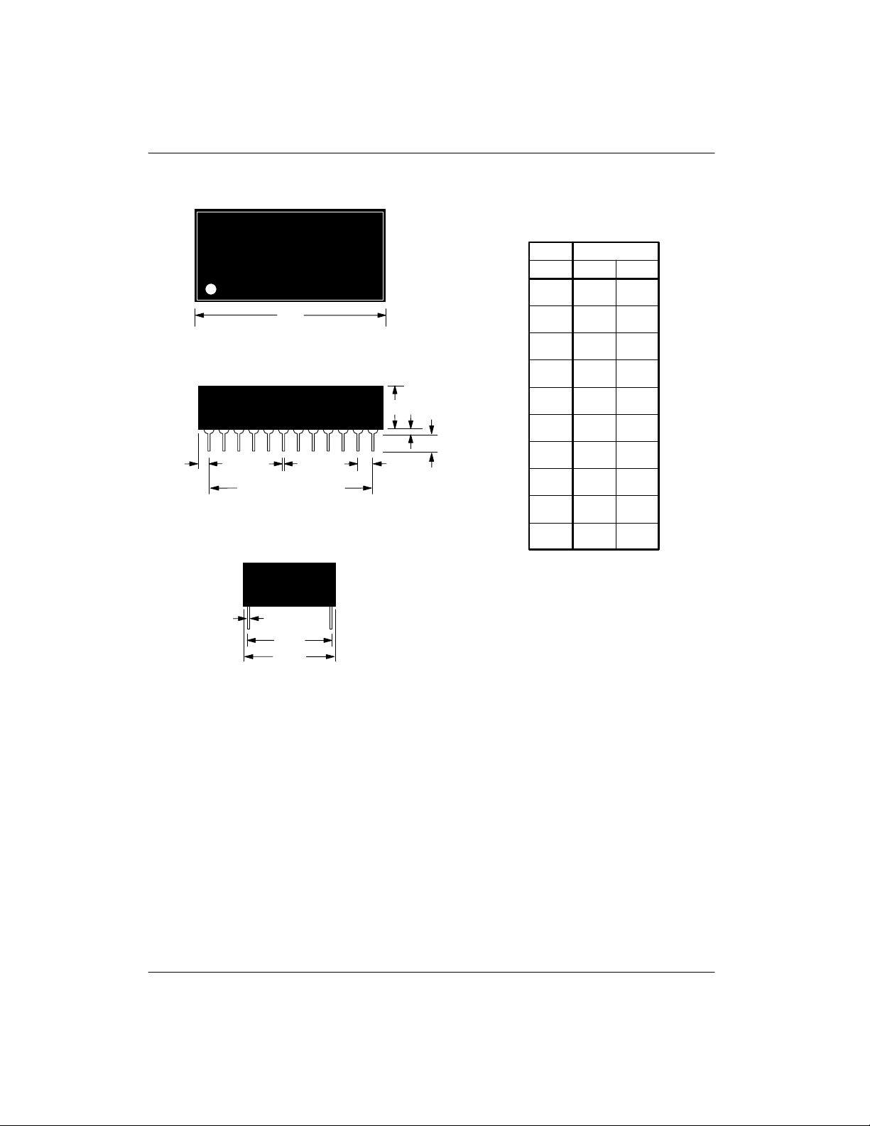
DS1387 24–PIN 740 MIL FLUSH ENCAPSULATED
24
112
A
KD
11 EQUAL SPACES AT
.100 .010 TNA
±
13
C E
F
G
24–PINPKG
DIM MIN MAX
A IN.
MM
B IN.
MM
C IN.
MM
D IN.
MM
E IN.
MM
F IN.
MM
G IN.
MM
H IN.
MM
J IN.
MM
K IN.
MM
1.320
33.53
0.720
18.29
0.345
8.76
0.100
2.54
0.015
0.38
0.110
2.79
0.090
2.29
0.590
14.99
0.008
0.20
0.015
0.38
1.335
33.91
0.740
18.80
0.370
9.40
0.130
3.30
0.030
0.89
0.140
3.56
0.110
2.79
0.630
16.00
0.012
0.30
0.021
0.53
012496 20/20
J
H
B
NOTE: PINS 2, 3, 16, AND 20 ARE MISSING BY DESIGN.
 Loading...