

Page 1
DS1603
TRI-STATE
General Description
The DS16033 is a dual differential TRI-STATE line receiver
designed for a broad range of system applications. It features ahigh input impedance and low input current which reduces theloading effectson adigital transmission line, making itideal for use in party line systems and generalpurpose
applications like transducer preamplifiers, level translators
and comparators.
The receivers feature a
±
over a
3V common mode range. Input protection diodes
are incorporated in series with the collectors of the differential stage. These diodes are useful in applications that have
multiple V
thus avoiding signal clamping. In addition, TTL compatible
strobe andcontrol lines are provide forflexibility in the application.
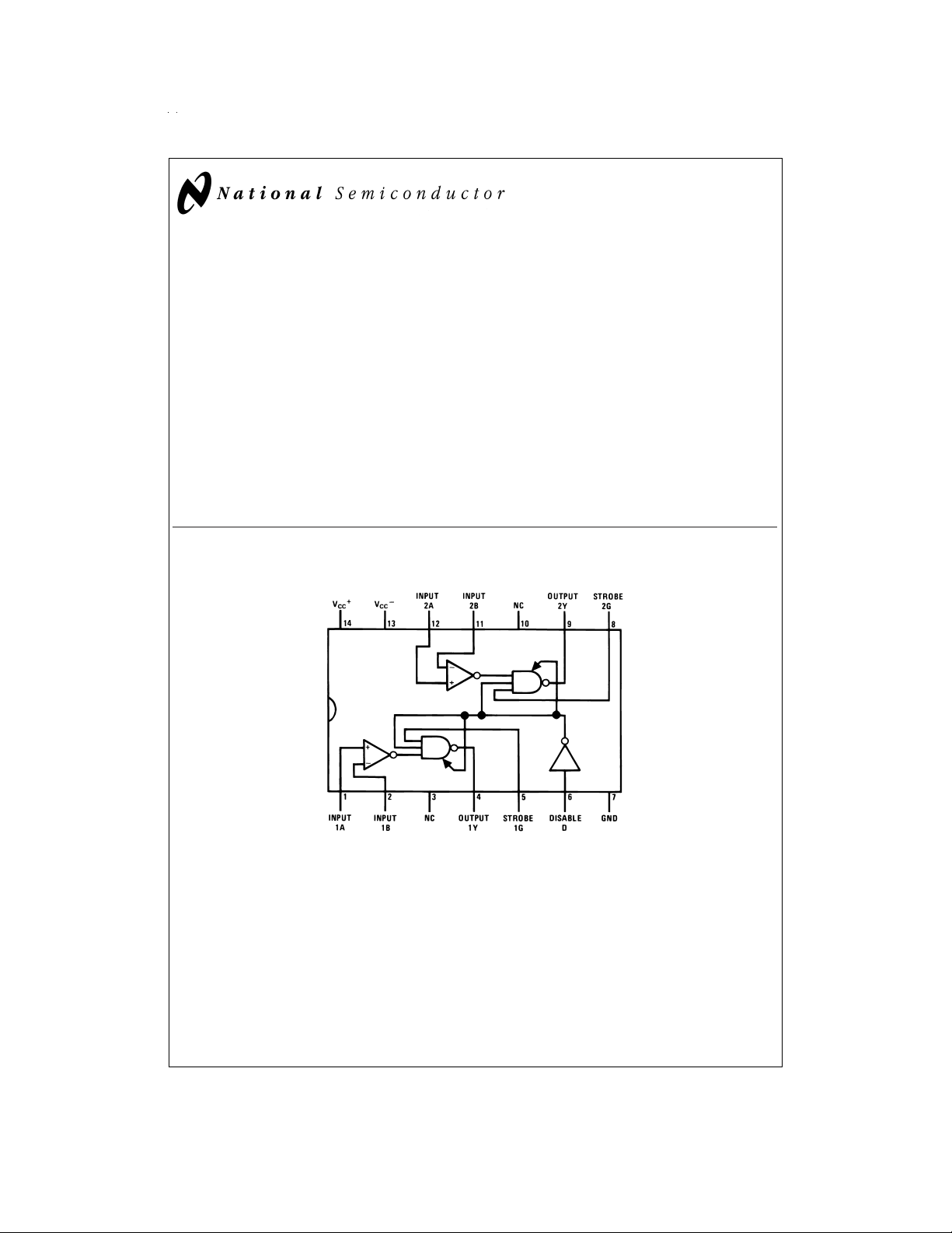
Connection Diagram
+ supplies or VCC+ supplies that are turned off
CC
®
Dual Receiver
±
25 mV input sensitivity specified
Dual-In-Line Package
May 1999
The DS1603 ispin compatible withthe DS75107 dualline receiver.
Features
n Diode protected input stage for power “OFF” condition
n 17 ns typ high speed
n TTL compatible
±
n
25 mV input sensitivity
±
n
3V input common-mode range
n High-input inpedance with normal V
n Strobes for channel selection
n TRI-STATE outputs for high speed buses
CC,
or V
=
0V
CC
DS1603TRI-STATE Dual Receiver
DS005781-2
For Complete Military 883 Specifications, See RETS Data Sheet.
Order Number: DS1603J/883 or DS1603W/883
See NS Package Number J14A
TRI-STATE®is a registered trademark of National Semiconductor Corporation.
© 1999 National Semiconductor Corporation DS005781 www.national.com
Top View
Page 2
Absolute Maximum Ratings (Note 2)
If Military/Aerospace specified devices are required,
please contact the National SemiconductorSales Office/
Distributors for availability and specifications.
Supply Voltage (V
Supply Voltage (V
Differential Input Voltage
+
)7V
CC
−
) −7V
CC
±
Common Mode Input Voltage
Strobe Input Voltage 5.5V
Storage Temperature Range −65˚C to +150˚C
Maximum Power Dissipation (Note 1) at 25˚C
Cavity Package 1308 mW
Molded Package 1207 mW
Lead Temperature (Soldering, 4 sec) 260˚C
6V
±
Operating Conditions
DS1603
Min Nom Max
Supply Voltage V
Supply Voltage V
+
CC
−
CC
4.5V 5V 5.5V
−4.5V −5V −5.5V
Operating Temperature Range −55˚C to +125˚C
Note 1: Derate cavity package 8.7 mW/˚C; derate molded package 9.7 mW/˚C above 25˚C.
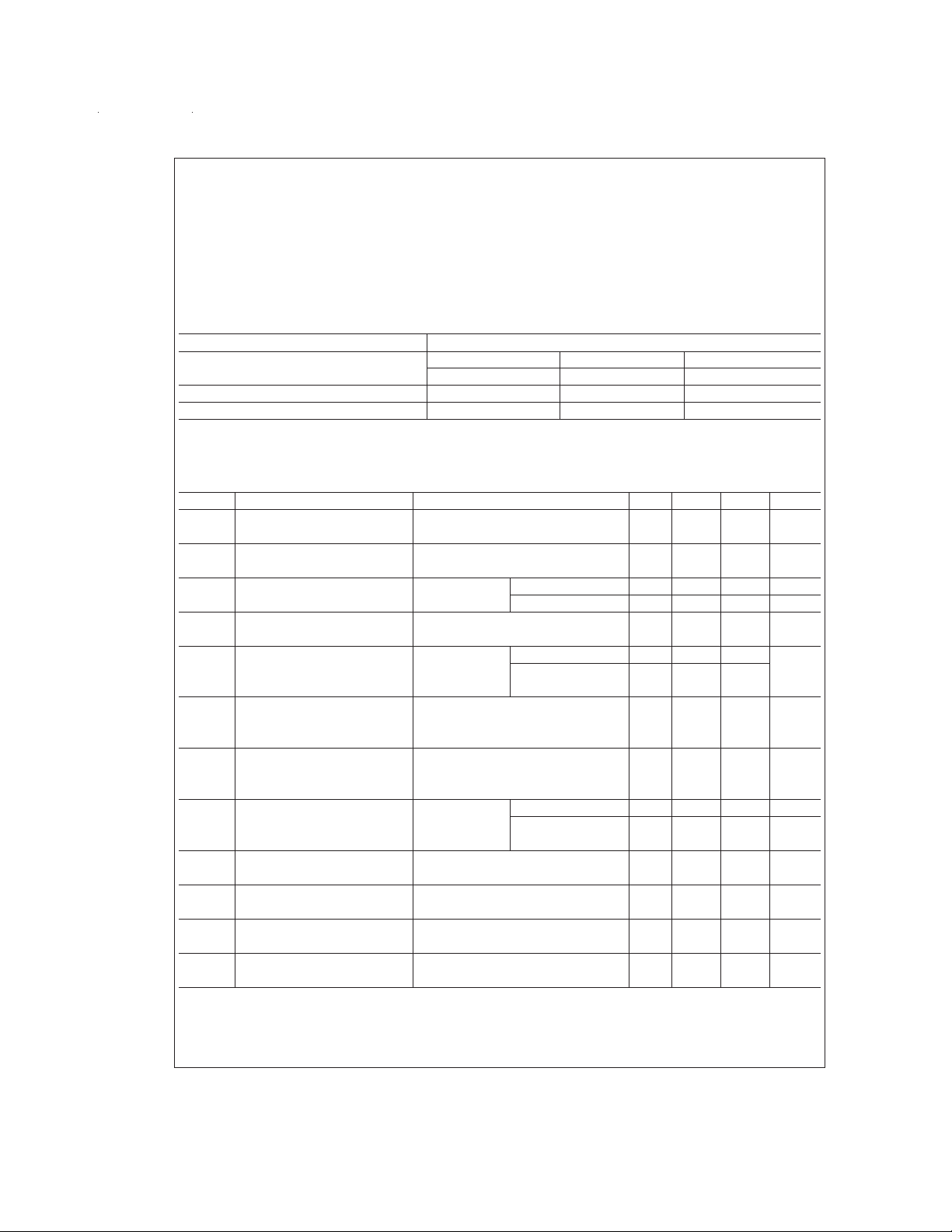
Electrical Characteristics (Notes 3, 4)
T
≤ TA≤ T
MIN
Symbol Parameter Conditions Min Typ Max Units
I
IH
I
IL
I
IH
I
IL
I
IL
V
OH
V
OL
I
OD
I
OS
+
I
CCH
−
I
CCH
V
I
Note 2: “AbsoluteMaximum Ratings” are those values beyond whichthesafetyof the device cannot be guaranteed. Exceptfor“OperatingTemperature Range” they
are not meant to imply that the devices should be operated at these limits. The table of “Electrical Characteristics” provides conditions for actual device operation.
Note 3: Unless otherwise specified min/max limits apply across the −55˚C to +125˚C temperature rangefor the DS1603and across the 0˚C to +70˚C range for the
DS3603. All typical values are for T
MAX
High Level Input Current V
into 1A, 1B, 2A or 2B V
Low Level Input Current V
into 1A, 1B, 2A or 2B V
High Level Input Current V
into 1G, 2G or D V
Low Level Input Current V
into D V
Low Level Input Current V
into 1G or 2G V
High Level Output Voltage V
Low Level Output Voltage V
Output Disable Current V
Short Circuit Output Current V
High Logic Level Supply V
Current from V
+
CC
High Logic Level Supply V
Current from V
−
CC
Input Clamp Voltage V
onGorD I
=
A
25˚C and V
=
5V.
CC
V
I
LOAD
V
I
SINK
V
V
V
V
V
V
IN
CC
ID
CC
ID
CC
CC
CC
IL(D)
CC
CC
IL(G)
CC
IL(D)
CC
IL(D)
CC
CC
IH(D)
CC
IL(D)
CC
ID
CC
ID
CC
+
=
Max, V
=
0.5V, V
+
=
Max, V
=
−2V, V
+
=
Max V
−
=
Max V
+
=
Max, V
=
0.4V
+
=
Max, V
−
=
Max, V
=
0.4V
+
=
Min, V
=
−2 mA, V
=
0.8V, V
+
=
Min, V
=
16 mA, V
=
0.8V, V
+
=
Max, V
−
=
Max, V
=
2V
+
=
Max, V
=
0.8V (Note 5)
+
=
Max, V
=
25 mV, T
+
=
Max, V
=
25 mV, T
+
=
Min, V
=
−12 mA, T
−
=
Max, 30 75 µA
CC
=
−3V to 3V
IC
−
=
Max, −10 µA
CC
=
−3V to 3V
IC
CC
CC
IC
CC
IC
CC
CC
A
CC
A
CC
A
=
2.4V 40 µA
IH(S)
=
IH(S)
−
=
Max, −1.6 mA
=
IH(D)
=
IL(D)
−
=
Min,
=
25 mV, 2.4 V
ID
=
−3V to 3V
−
=
Min,
=
−25 mV, 0.4 V
ID
=
−3V to 3V
=
OUT
=
OUT
−
=
Max, −18 −70 mA
−
=
Max, 28 40 mA
=
25˚C
−
=
Max, −8.4 −15 mA
=
25˚C
−
=
Min, −1 −1.5 V
=
25˚C
+
Max V
CC
2V −40 µA
0.8V −1.6 mA
2.4V 40 µA
0.4V −40 µA
1mA
5V
www.national.com 2
Page 3

Electrical Characteristics (Notes 3, 4) (Continued)
Note 4: All current into device pins shown as positive, out of device pins as negative, all voltages referenced to ground unless otherwise noted. All values shown
as max or min on absolute value basis.
Note 5: Only one output at a time should be shorted.
Switching Characteristics
+
=
V
CC
Symbol Parameter Conditions Min Typ Max Units
t
PLH(D)
t
PHL(D)
t
PLH(S)
t
PHL(S)
t
1H
t
0H
t
H1
t
H0
Note 6: Differential input is +100 mV to −100 mV pulse. Delays read from 0 mV on input to 1.5V on output.
−
5V, V
=
CC
Propagation Delay Time, Low-to- R
−5V, T
=
25˚C
A
=
L
390Ω,C
=
50 pF, (Note 6)
L
High Level, from Differential 17 25 ns
Inputs A and B to Output
Propagation Delay Time, High-to- R
=
L
390Ω,C
=
50 pF, (Note 6)
L
Low Level, from Differential 17 25 ns
Inputs A and B to Output
Propagation Delay Time, Low-to- R
=
L
390Ω,C
=
50 pF
L
High Level, from Strobe Input G 10 15 ns
to Output
Propagation Delay Time, High-to- R
=
L
390Ω,C
=
50 pF
L
Low Level, from Strobe Input G 8 15 ns
to Output
Disable Low-to-High to Output R
=
L
390Ω,C
=
5pF 20 ns
L
High to Off
Disable Low-to-High to Output R
=
L
390Ω,C
=
5pF 30 ns
L
Low to Off
Disable High-to-Low to Output R
=
1k to 0V, C
L
=
50 pF 25 ns
L
Off to High
Disable High-to-Low to Output R
=
L
390Ω,C
=
50 pF 25 ns
L
Off to Low
www.national.com3
Page 4
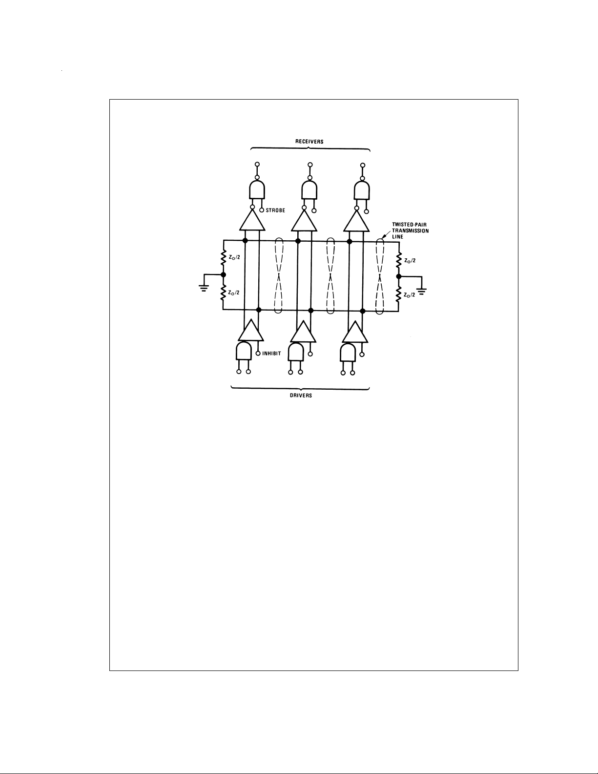
Typical Application
Line Receiver Used in a Party-Line or Data-Bus System
Line receivers are
DS75107/DS75108
or DS3603
Line drivers are
SN75109/µA75110/DS75110
or DS8831
www.national.com 4
DS005781-3
Page 5
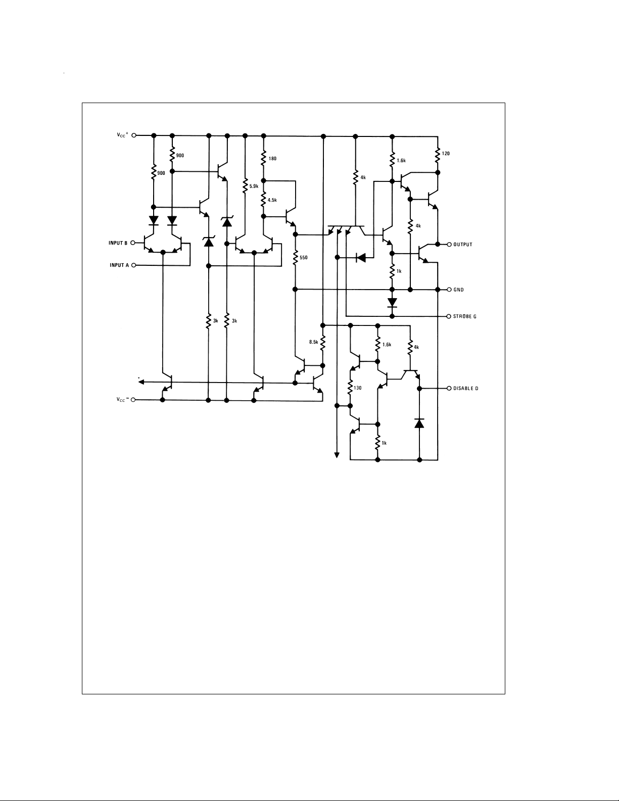
Schematic Diagram (Note 7)
Note 7:1⁄2of the dual circuit is shown.
*
Note 8:
Indicates connections common to second half of dual circuit.
DS005781-6
www.national.com5
Page 6
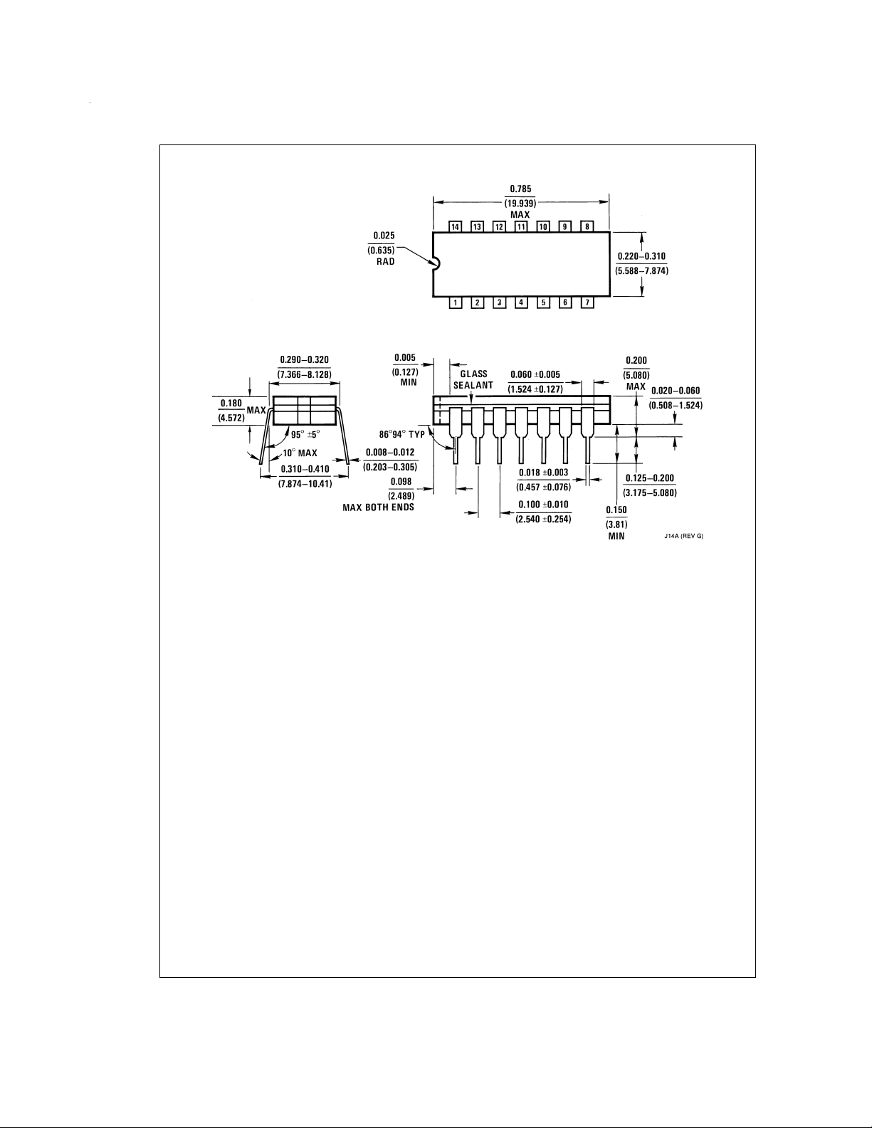
Physical Dimensions inches (millimeters) unless otherwise noted
Ceramic Dual-In-Line Package (J)
Order Number DS1603J
NS Package Number J14A
www.national.com 6
Page 7
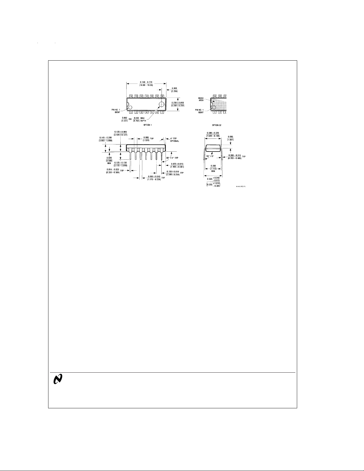
Physical Dimensions inches (millimeters) unless otherwise noted (Continued)
Molded Dual-In-Line Package (N)
Order Number DS3603N
NS Package Number N14A
DS1603TRI-STATE Dual Receiver
LIFE SUPPORT POLICY
NATIONAL’S PRODUCTS ARE NOT AUTHORIZED FOR USE AS CRITICAL COMPONENTS IN LIFE SUPPORT
DEVICES OR SYSTEMS WITHOUT THE EXPRESS WRITTEN APPROVAL OF THE PRESIDENT AND GENERAL
COUNSEL OF NATIONAL SEMICONDUCTOR CORPORATION. As used herein:
1. Life support devices or systems are devices or
systems which, (a) are intended for surgical implant
into the body, or (b) support or sustain life, and
whose failure to perform when properly used in
accordance with instructions for use provided in the
2. A critical component is any component of a life
support device or system whose failure to perform
can be reasonably expected to cause the failure of
the life support device or system, or to affect its
safety or effectiveness.
labeling, can be reasonably expected to result in a
significant injury to the user.
National Semiconductor
Corporation
Americas
Tel: 1-800-272-9959
Fax: 1-800-737-7018
Email: [email protected]
www.national.com
National does not assume any responsibility for use of any circuitry described, no circuit patent licenses are implied and National reserves the right at any time without notice to change said circuitry and specifications.
National Semiconductor
Europe
Fax: +49 (0) 1 80-530 85 86
Email: [email protected]
Deutsch Tel: +49 (0) 1 80-530 85 85
English Tel: +49 (0) 1 80-532 78 32
Français Tel: +49 (0) 1 80-532 93 58
Italiano Tel: +49 (0) 1 80-534 16 80
National Semiconductor
Asia Pacific Customer
Response Group
Tel: 65-2544466
Fax: 65-2504466
Email: [email protected]
National Semiconductor
Japan Ltd.
Tel: 81-3-5639-7560
Fax: 81-3-5639-7507
 Loading...