

Page 1
DS14C238
Single Supply TIA/EIA-2324x4Driver/Receiver
DS14C238 Single Supply TIA/EIA-2324x4Driver/Receiver
May 1999
General Description
The DS14C238 is a four driver, four receiver device which
conforms to the TIA/EIA-232-E standard and CCITT V.28
recommendations. This device eliminates
employing an internal DC-DCconverter to generate the necessary output levels from a single +5V supply. Driver slew
rate control and receiver noise filtering have also been internalized to eliminate the need for external slew rate control
and noise filtering capacitors.
±
12V supplies by
Features
n Conforms to TIA/EIA-232-E and CCITT V.28
n Internal DC-DC converter
n Operates with single +5V supply
n Low power requirement—I
n Internal driver slew rate control
n Receiver noise filtering
n Operates above 120 kbits/sec
n Direct replacement for MAX238
CC
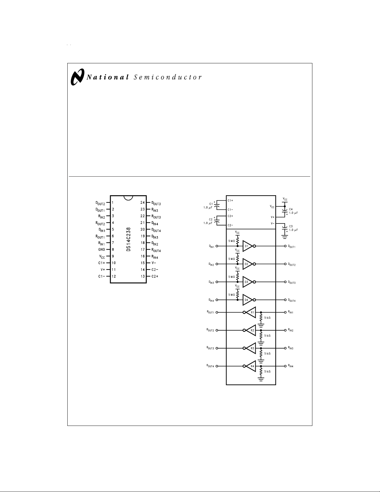
Connection Diagram Functional Diagram
DS011282-1
Order Number DS14C238WM
See NS Package Number M24B
10 mA max
DS011282-2
© 1999 National Semiconductor Corporation DS011282 www.national.com
Page 2
Absolute Maximum Ratings (Note 1)
If Military/Aerospace specified devices are required,
please contact the National Semiconductor Sales Office/
Distributors for availability and specifications.
Supply Voltage (V
V+ Pin (V
V− Pin +0.3V to −15V
Driver Input Voltage −0.3V to (V
Driver Output Voltage (V+ +0.3V) to (V−
Receiver Input Voltage
Receiver Output Voltage −0.3V to (V
Junction Temperature +150˚C
Maximum Package Power Dissipation
) −0.3V to +6V
CC
−0.3V) to +15V
CC
@
+25˚C (Note 6)
CC
CC
+0.3V)
−0.3V)
±
30V
+0.3V)
Lead Temp.
(Soldering, 4 Seconds) +260˚C
Short Circuit Duration
) Continuous
(D
OUT
ESD Rating
(HBM, 1.5 kΩ, 100 pF) ≥ 2.0 kV
Recommended Operating
Conditions
Min Max Units
Supply Voltage, V
Operating Free Air Temp. (T
DS14C238 0 +70 ˚C
4.5 5.5 V
CC
)
A
WM Package 1400 mW
Storage Temp. Range −65˚C to +150˚C
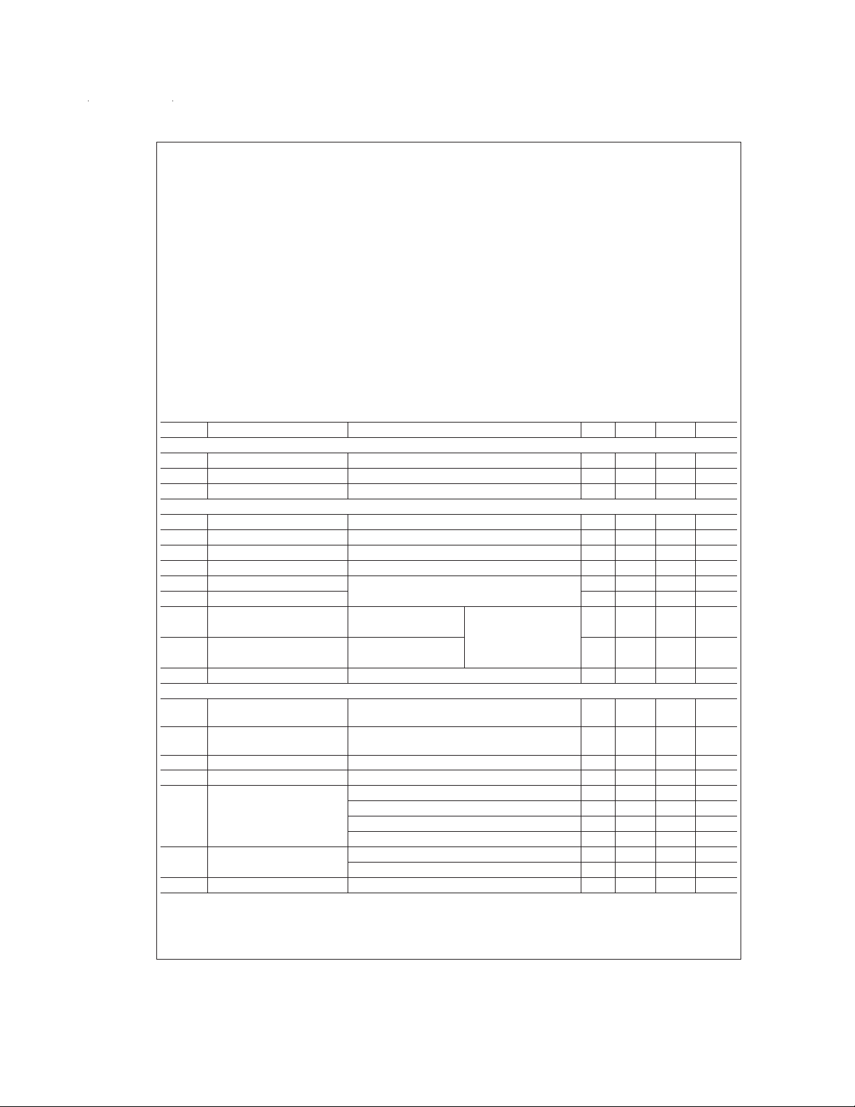
Electrical Characteristics (Note 2)
Over recommended operating conditions, unless otherwise specified.
Symbol Parameter Conditions Min Typ Max Units
DEVICE CHARACTERISTICS
V+ Positive Power Supply R
V− Negative Power Supply R
I
CC
Supply Current (VCC) No Load 7.0 10 mA
DRIVER CHARACTERISTICS
V
IH
V
IL
I
IH
I
IL
V
OH
V
OL
I
OS
High Level Input Voltage 2.0 V
Low Level Input Voltage GND 0.8 V
High Level Input Current VIN≥ 2.0V −10 +10 µA
Low Level Input Current VIN≤ 0.8V −10 +10 µA
High Level Output Voltage RL=3kΩ 5.0 7.4 V
Low Level Output Voltage −6.3 −5.0 V
+ Output High Short VO= 0V, VIN= 0.8V (Note 3) −30 −15 −5.0 mA
Circuit Current
I
− Output Low Short VO= 0V, VIN= 2.0V 5.0 12 30 mA
OS
Circuit Current
R
O
Output Resistance −2V ≤ VO≤ +2V, VCC= GND = 0V 300 Ω
RECEIVER CHARACTERISTICS
V
TH
V
TL
V
HY
R
IN
I
IN
V
OH
V
OL
Input High Threshold
Voltage
Input Low Threshold
Voltage
Hysteresis 0.2 0.4 1.0 V
Input Resistance 3.0 4.5 7.0 kΩ
Input Current VIN= +15V 2.14 3.8 5.0 mA
High Level Output Voltage VIN= −3V, IO= −3.2 mA 3.5 4.5 V
Low Level Output Voltage VIN= +3V, IO= +2.0 mA 0.25 0.4 V
=3kΩ, C1–C4 = 1.0 µF, DIN= 0.8V 9.0 V
L
=3kΩ, C1–C4 = 1.0 µF, DIN= 2.0V −8.0 V
L
CC
1.9 2.4 V
0.8 1.5 V
V
= +3V 0.43 0.6 +1.0 mA
IN
V
= −3V −1.0 −0.6 −0.43 mA
IN
V
= −15V −5.0 −3.8 −2.14 mA
IN
V
= −3V, IO= −20 µA 4.0 4.9 V
IN
V
www.national.com 2
Page 3

Switching Characteristics (Note 4)
Over recommended operating conditions, unless otherwise specified.
Symbol Parameter Conditions Min Typ Max Units
DRIVER CHARACTERISTICS
t
PLH
t
PHL
t
sk
SR1 Output Slew Rate R
SR2 Output Slew Rate R
Propagation Delay LOW to HIGH RL=3kΩ 0.7 4.0 µs
Propagation Delay HIGH to LOW CL= 50 pF 0.6 4.0 µs
Skew |t
PLH–tPHL
|(
Figures 1, 2
L
L
) 0.1 1.0 µs
=3kΩto7kΩ,CL= 50 pF 4.0 15 30 V/µs
=3kΩ,CL= 2500 pF 3.0 5.0 V/µs
RECEIVER CHARACTERISTICS
t
PLH
t
PHL
t
SK
t
NW
Note 1: “Absolute Maximum Ratings” are those values beyond which the safety of the device cannot be guaranteed. They are not meant to imply that the devices
should be operated at these limits. The tables of “Electrical Characteristics” specify conditions for device operation.
Note 2: Current into device pins is defined as positive. Current out of device pins is defined as negative. All voltages are referenced to ground unless otherwise specified.
Note 3: I
Note 4: Receiver AC input waveform for test purposes: t
t
r=tf
Note 5: All typicals are given for V
Note 6: Ratings apply to ambient temperature at +25˚C. Above this temperature derate: WM package 13.5 mW/˚C.
Propagation Delay LOW to HIGH Input Pulse Width>10 µs 2.0 6.5 µs
Propagation Delay HIGH to LOW CL= 50 pF 2.8 6.5 µs
Skew | t
PLH–tPHL
Noise Pulse Width Rejected (
+ and IOS− values are for one output at a time. If more than one output is shorted simultaneously, the device power dissipation may be exceeded.
OS
≤10 ns, VIH=3V,VIL=0V,f=64kHz(128 kbits/sec).
|(
= 5.0V and TA= +25˚C.
CC
Figures 3, 4
Figures 3, 4
= 200 ns, VIH=3V,VIL=−3V,f=64kHz(128 kbits/sec). Driver AC input waveform for test purposes:
r=tf
) 0.8 2.0 µs
) 2.5 1.0 µs
Parameter Measurement Information
DS011282-4
FIGURE 1. Driver Load Circuit
FIGURE 2. Driver Switching Waveform
DS011282-6
FIGURE 3. Receiver Load Circuit
DS011282-5
www.national.com3
Page 4

Parameter Measurement Information (Continued)
FIGURE 4. Receiver Propagation Delays and Noise Rejection
Pin Descriptions
VCC(pin 9) — Power supply pin for the device,
±
10%).
+5V (
V+ (pin 11)— Positive supply for TIA/EIA-232-E drivers.
Recommended external capacitor: C4 = 1.0 µF (6.3V). This
supply is not intended to be loaded externally.
V− (pin 15) — Negative supply for TIA/EIA-232-E drivers.
Recommended external capacitor: C3 = 1.0 µF (16V). This
supply is not intended to be loaded externally.
C1+, C1− (pins 10 and 12) — External capacitor connection
pins. Recommended capacitor – 1.0 µF (6.3V).
C2+, C2− (pins 13 and 14)— External Capacitor connection pins. Recommended capacitor – 1.0 µF (16V).
D
1–4 (pins 5, 18, 19, and 21)— Driver input pins are
IN
TTL/CMOS compatible. Inputs of unused drivers may be left
open, an internal pull-up resistor (500 kΩ minimum, typically
5MΩ) pulls input to V
D
OUT
form to TIA/EIA-232-E levels.
R
IN1
cept TIA/EIA-232-E input voltages (
ture a noise filter and guaranteed hysteresis of 200 mV. Unused receiver input pins may be left open. Internal input
resistor (5 kΩ) pulls input LOW, providing a failsafe HIGH
output.
R
OUT
are TTL/CMOS compatible. Receiver output HIGH voltage is
specified for both CMOS and TTL load conditions.
GND (pin 8) — Ground Pin.
DS011282-7
. Output will be LOW for open inputs.
CC
1–4 (pins 2, 1, 24, and 20) — Driver output pins con-
1–4 (pins 3, 7, 23, and 16) — Receiver input pins ac-
±
15V). Receivers fea-
1–4 (pins 4, 6, 22, and 17) — Receiver output pins
www.national.com 4
Page 5

Physical Dimensions inches (millimeters) unless otherwise noted
Order Number DS14C238WM
NS Package Number M24B
DS14C238 Single Supply TIA/EIA-2324x4Driver/Receiver
LIFE SUPPORT POLICY
NATIONAL’S PRODUCTS ARE NOT AUTHORIZED FOR USE AS CRITICAL COMPONENTS IN LIFE SUPPORT
DEVICES OR SYSTEMS WITHOUT THE EXPRESS WRITTEN APPROVAL OF THE PRESIDENT AND GENERAL
COUNSEL OF NATIONAL SEMICONDUCTOR CORPORATION. As used herein:
1. Life support devices or systems are devices or
systems which, (a) are intended for surgical implant
into the body, or (b) support or sustain life, and
whose failure to perform when properly used in
accordance with instructions for use provided in the
2. A critical component is any component of a life
support device or system whose failure to perform
can be reasonably expected to cause the failure of
the life support device or system, or to affect its
safety or effectiveness.
labeling, can be reasonably expected to result in a
significant injury to the user.
National Semiconductor
Corporation
Americas
Tel: 1-800-272-9959
Fax: 1-800-737-7018
Email: support@nsc.com
www.national.com
National does not assume any responsibility for use of any circuitry described, no circuit patent licenses are implied and National reserves the right at any time without notice to change said circuitry and specifications.
National Semiconductor
Europe
Fax: +49 (0) 1 80-530 85 86
Email: europe.support@nsc.com
Deutsch Tel: +49 (0) 1 80-530 85 85
English Tel: +49 (0) 1 80-532 78 32
Français Tel: +49 (0) 1 80-532 93 58
Italiano Tel: +49 (0) 1 80-534 16 80
National Semiconductor
Asia Pacific Customer
Response Group
Tel: 65-2544466
Fax: 65-2504466
Email: sea.support@nsc.com
National Semiconductor
Japan Ltd.
Tel: 81-3-5639-7560
Fax: 81-3-5639-7507
 Loading...