

Page 1
DPL 4519G
Sound Processor for
Digital and Analog
Edition Oct. 31, 2000
6251-512-1PD
PRELIMINARY DATA SHEET
MICRONAS
MICRONAS
Surround Systems
Page 2

DPL 4519G PRELIMINARY DATA SHEET
Contents
Page Section Title
4 1. Introduction
5 1.1. Features of the DPL 4519G
6 1.2. Application Fields of the DPL 4519G
7 2. Functional Description
7 2.1. Architecture of the DPL 4519G Family
8 2.2. Preprocessing I
8 2.3. Selection of Internal Processed Surround Signals
8 2.4. Source Selection and Output Channel Matrix
8 2.5. Audio Baseband Processing
8 2.5.1. Main and Aux Outputs
8 2.6. Surround Processing
8 2.6.1. Surround Processing Mode
8 2.6.1.1. Decoder Matrix
9 2.6.1.2. Surround Reproduction
9 2.6.1.3. Center Modes
9 2.6.1.4. Useful Combinations of Surround Processing Modes
10 2.6.2. Examples
11 2.6.3. Application Tips for using 3D-PANORAMA
11 2.6.3.1. Sweet Spot
11 2.6.3.2. Clipping
11 2.6.3.3. Loudspeaker Requirem ents
11 2.6.3.4. Cabinet Requirements
11 2.6.4. Input and Output Levels for Dolby Surround Pro Logic
11 2.7. SCART Signal Routing
11 2.7.1. SCART Out Select
12 2.7.2. Stand-by Mode
2
12 2.8. I
S Bus Interfaces
12 2.8.1. Synchronous I
12 2.8.2. Asynchronous I
12 2.8.3. Multichannel I
12 2.8.4. Asynchronous Multichannel I
13 2.9. Digital Control I/O Pins
13 2.10. Clock PLL Oscillator and Crystal Specifications
2
S Input Signals
2
S-Interface(s)
2
S-Interface
2
S-Output
2
S-Input
14 3. Control Interface
2
14 3.1. I
C Bus Interface
14 3.1.1. Device and Subaddresses
14 3.1.2. Internal Hardware Error Handling
15 3.1.3. Description of CONTROL Register
15 3.1.4. Protocol Description
2
16 3.1.5. Proposals for General DPL 4519G I
C Telegrams
16 3.1.5.1. Symbols
16 3.1.5.2. Write Telegrams
16 3.1.5.3. Read Telegrams
16 3.1.5.4. Examples
2
16 3.2. Start-Up Sequence: Power-Up and I
C Controlling
2 Micronas
Page 3

PRELIMINARY DATA SHEET
Contents, continued
Page Section Title
16 3.3. DPL 4519G Programming Interface
16 3.3.1. User Registers Overview
19 3.3.2. Description of User Registers
2
19 3.3.2.1. Write Registers on I
21 3.3.2.2. Read Registers on I2C Subaddress 11
21 3.3.2.3. Write Registers on I2C Subaddress 12
33 3.3.2.4. Read Registers on I2C Subaddress 13
C Subaddress 10
hex
hex
hex
hex
34 3.4. Programming Tips
34 3.5. Examples of Minimum Initialization Codes
34 3.5.1. Micronas Dolby Digital chipset (with MAS 3528E)
35 4. Specifications
35 4.1. Outline Dimensions
37 4.2. Pin Connections and Short Descriptions
40 4.3. Pin Descriptions
43 4.4. Pin Configurations
45 4.5. Pin Circuits
47 4.6. Electrical Characteristics
47 4.6.1. Absolute Maximum Ratings
48 4.6.2. Recommended Operating Conditions (T
= 0 to 70 °C)
A
48 4.6.2.1. General Recommended Operating Conditions
48 4.6.2.2. Analog Input and Output Recommendations
49 4.6.2.3. Crystal Recommendations
50 4.6.3. Characteristics
50 4.6.3.1. General Characteristic s
51 4.6.3.2. Digital Inputs, Digital Outputs
52 4.6.3.3. Reset Input and Power-Up
2
53 4.6.3.4. I
54 4.6.3.5. I
C-Bus Characteristics
2
S-Bus Characteristics
56 4.6.3.6. Analog Baseband Inputs and Outputs, AGNDC
58 4.6.3.7. Power Supply Rejection
58 4.6.3.8. Analog Performance
DPL 4519G
61 5. Appendix A: Application Information
61 5.1. Phase Relationship of Analog Outputs
62 5.2. Application Circuit
64 6. Data Sheet History
License Notice:
“Dolby Pro Logic” and “Dolby Digital” are trademarks of Dolby Laboratories.
Supply of this implementation of Dolby T echnolog y does not conv ey a license nor imply a right under any patent, or any other industrial or intellec-
tual property right of Dolby Laboratories, to use this implementation in any finished end-user or ready-to-use final product. Companies planning to
use this implementation in products must obtain a license from Dolby Laboratories Licensing Corporation before designing such products.
Micronas 3
Page 4
DPL 4519G PRELIMINARY DATA SHEET
Sound Processor for Digital and Analog Surround
Systems
The hardware and software description in this document is valid for the DPL 4519G version A1 and following versions.
1. Introduction
The DPL 4519G processor is designed as par t of the
Micronas chip set for digital a nd analog Surroun d S ystems i. e. Dolby Digital, MPEG 2 Audio, or Dolby ProLogic. The combination of MAS 3528E, DPL 4519G,
and MSP 44x0G is a complete 5.1 channel Dolby Digital decoder and playback solution, while DPL 4519G
and MSP 44x0G alone, represent a complete Dolby
Surround Pro Logic system.
The DPL 4519G receives its incomi ng data via highly
flexible I
can be configured as three asynchronous I
2
S interfaces. The three I2S input interfaces
2
S inputs or
two synchronous a nd one asynchronous in terface. In
the latter case, the asynchronous interface allows
reception of 2-8 channels with arbitrary sample rate
ranging from 8 to 48 kHz. The synchronization is performed by means of an adaptive high-quality sample
rate converter.
In an application together with the Dolby Digital
decoder MAS 3528E, eight channels (left, right, surround left, surround r ig ht, c ent er, subwoofer, Pro Logic
encoded left, Pro Logic encoded right) are fed in and
processed in the DPL 4519G.
Similar to the multichannel I
is provided with an 8-channel I
2
S input interface, the DPL
2
S output interface,
which can be conne cted to a MSP 44x0G. Therefore
all 8 channels can be routed to each output in both
ICs.
The baseband processing including e.g. balance,
bass, treble, and loudness is performed at a fixed sample rate of 48 kHz.
Fig. 1–1 shows a simplified functional block diagram of
the DPL 4519G.
The DPL 4519G is pin-compatible to members of the
MSP 34xx family. This speeds up PCB development
for customers using MSPs.
The software interface of the DPL 4519G is also
largely the same as for members of the MSP family.
The ICs are prod uc ed in s ub mi cro n CM O S tec hn ology
and are available in PQFP80, PLQFP64 and in
PSDIP64 packages.
I2S1
I2S2
I2S3
SCART1
SCART2
SCART3
SCART4
MONO
I2S
I2S
Prescale
I2S
(2..8-channel)
ProLogic
processing
Fig. 1–1: Simplified block diagram of the DPL 4519G
Source Select
Main
Sound
Processing
AUX
Sound
Processing
DAC
DAC
DAC
SCART
Output
Select
Main
Subwoofer
AUX
I2S
(8-channel)
SCART1
SCART2
4 Micronas
Page 5

PRELIMINARY DATA SHEET DPL 4519G
1.1. Features of the DPL 4519G
2
– 8-channel asynchonou s I
+ 2 synchronous I
2
S input channels (e.g. for MSP and ADR)
S input interface (multichannel mode)
or
2
3 asynchronous two-channel I
S input interfaces
– Main and AUX channel with balance, bass, treble, loudness, volume
– 5-band graphic equalizer for Main channel
– Dolby Surround Pro Logic Adaptive Matrix
– Micronas Effect Matrix
– Micronas “3D-Panorama” virtualizer compliant to “Virtual Dolby Surround” technology
– Micronas Panorama sound mode (3D Surround sound via two loudspeakers)
– Noise Generator
– Spatial Effect for Surround
– 30-ms Surround delay
– Surround matrix control: Adaptive/Passive/Effect
– Center mode control: Normal/Phantom/Wide/Off
– Surround reproduction control: Rear speaker, Front speaker, Panorama, 3D-Panorama
2
– Two digital input/output pins controlled by I
C bus
Fig. 1–2 shows a typical Dolby Digital application using DPL 4519G, MSP 4450G, and MAS 3528E.
Micronas 5
Page 6
DPL 4519G PRELIMINARY DATA SHEET
1.2. Application Fields of the DPL 4519G
S/PDIF In 1/2
AC-3, MPEG L2, PCM or other Format
I2S-In: Slave
18.432 MHz
18.432
MHz
Dolby
Digital
Upgrade
Module
Basic
TV-
Sound
System
18.432
MHz
S/PDI1
S/PDI2
SID*
SII*
SIC*
SID
SII
SIC
I2S_WS3
I2S_CL3
AUDIO_
CL_OUT
I2S_WS
I2S_CL
I2S_WS3
I2S_CL3
I2S_WS
I2S_CL
Input
Buffer
Amp./
Osc.
I2S_Inputs
123
2-8 Ch. Input
(LT, RT,L, R
S
, SR,C, SUB)
L
6 Channel
Loop-through
Dolby
Pro Logic
Decoder
I2S_Inputs
123
2-8
Channel
Serial
Input
PCM
MPEG
Deemphasis
AC-3
Noise
Gen.
PLL Synth.
CLKO
I2S-Mode:Multichannel Mode auf D0
(6 - 8 Channels, fs=32, 44.1 or 48 kHz,
I2S_1_L
I2S_1_R
I2S_2_L
I2S_2_R
I2S_3_L
I2S_3_R
16,18,....32 Bit)
t
t
L
R
or
S
L
S
R
C
SUB
Dolby Digital: (Lt, Rt, L, R, SL, SR, C, SUB)
Pro Logic: (L
I2S_1_L
I2S_1_R
I2S_2_L
I2S_2_R
I2S_3_L
t
I2S_3_R
t
I2S_3_L
I2S_3_R
I2S_3_S
L
I2S_3_S
R
I2S_3_C
I2S_3_SUB
L
2
R
Ls
Rs
C/
Sub
Delay Lines
Lt
Post Processing
Rt
MAS 3528E
Dolby Digital Decoder
MPEG-L2 Decoder
Bass
Treble
Balance
Volume
Bass
Treble
Balance
Volume
Volume
DPL 4519G
Pro Logic Decoder
, Rt, L, R, C, SubW)
t
Sound-
Process.
Balance
Volume
Bass
Treble
Balance
Volume
Volume D/A
Volume
Multipl.
analog
Volume
analog
Volume
D/A
analog
Volume
analog
Volume
D/A
D/A
D/A
D/A
D/A
SPDO
SOD3
SOD2
SOD1
SOD
SOI
SOC
S/PDIF Out
PCM-Format (Lt/Rt or L/R or Lo/Ro)
or Loop-through (e.g. DTS)
Dolby Digital / Pro Logic Configurations
Example 1:
- internal L, C, R
- internal woofer for low freq. of L, (C), R
- ext. Surround speakers S
- ext. Subwoofer for SUB channel.
Example 2:
- internal Left and Right used as C
- internal woofer for low freq. of C
- ext. L, R
- ext. Surround speakers S
- ext. Subwoofer for SUB channel.
Configuration Examples
normal
Main
---
---
SUB
(C
Aux
SCART1
I2S_Out_L/R
Main
Aux
SCART1
SCART2
---
---
---
---
---
Subw
C, SUB
SL, SR
L
L
Subw
R
L
R
L
R
L
R
, S
L
R
, S
L
R
Dolby Digital /
Pro Logic
12
C
L
ext
int
SUB
ext
ext
R
)---
ext
int
S
S
L
S
R
L, R
t
L
R
R
R
R
L
, R
L
L
L
L
S
R
R
L
t
t
R
t
t
L, R
C, SUB
SL, SR
L
, R
t
t
t
C
int
int
Subw
int
int
C
int
int
L
t
t
R
t
t
L
t
t
R
t
t
L
t
t
R
t
t
2
SIF-IN
SCART1_In
SCART4_In
Demod
.
.
.
A/D
MSP 4450G
I2S_Out_L/R
L, R
L, R
L, R
Multistandard Sound Processor
Fig. 1–2: Typical DPL 4519G application
6 Micronas
Page 7
PRELIMINARY DATA SHEET DPL 4519G
2. Functional Description
2.1. Architecture of the DPL 4519G Family
Fig. 2–1 shows a simplified block diagram of the IC.
(sync. 48kHz)
DACM_R
DACM_L
D
Volume
)
hex
(01
Balance
Bass/
Tre ble/
Main
Channel
Σ
Loudness/
Matrix
DACM_SUB
A
)
hex
(00
)
hex
(2C
Adjust
fer Level
Subwoo-
Beeper
)
)
hex
hex
)
(14
hex
Equalizer
(02/03/04
(20..25
)
hex
(08
DACA_R
DACA_L
A
D
Volume
)
Balanc
(30
Σ
Bass/
Tre ble/
Loudness
Aux
Matrix
Channel
I2S_DA_OUT
I2S
)
Interface
hex
(06
hex
)
hex
(31/32/33
S
2
I
)
hex
(09
Channel
)
Matrix
hex
(0B
SCART1_L/R
A
D
)
hex
(07
Volume
)
Matrix
SCART1
Channel
Matrix
Channel
hex
Surround
(0A
SC1_OUT_L
SC1_OUT_R
)
hex
(48
SC2_OUT_L
SC2_OUT_R
SCART Output Select
Source Select
5
S1
2
I
6
)
hex
(16
Prescale
)
hex
(12
S2
2
I
Prescale
7
t
L
8
L
t
L
R
S3
2
I
9
L
R
S
L
R
S
S
I2S_3 Resorting Matrix
Prescale
10
R
C
S
Internal/External Switch
R
SUB
)
)
)
hex
(36
C
SUB
)
hex
(36
)
hex
(11
Surround
Noise
Processing
Generator
)
)
hex
hex
hex
hex
(4B
(4C
(49
(4A
)
hex
(4D
synchronization
S
2
I
Interface
I2S_DA_IN1
(sync. 48kHz)
S
2
I
Interface
I2S_CL
I2S_WS
I2S_DA_IN2
(sync. 48kHz)
S
2
I
Interface
I2S_CL3
I2S_WS3
I2S_DA_IN3
(async. 8-48 kHz)
SC2_IN_L
SC1_IN_L
SC2_IN_R
SC1_IN_R
SC4_IN_L
SC3_IN_L
SC3_IN_R
MONO_IN
SC4_IN_R
Micronas 7
Fig. 2–1: Signal flow block diagram of the DPL 4519G (input and output names correspond to pin names)
Page 8

DPL 4519G PRELIMINARY DATA SHEET
2.2. Preprocessing I2S Input Signals
2
S inputs can be adjusted in level by means of the
The I
2
S prescale registers.
I
2
S_3 interface is able to receive more tha n two
The I
channels (see Sect ion 2.6. on page 8) . The incoming
signals can be resor ted by a programmable matrix in
order to obtain a certain order, which means an unified
postprocessing afterwards.
2
Since the I
S_3 interface is asynchronous, incoming
sound signals with arbi trary sampl e rates in the range
of 8-48 kHz are in terpolated to 4 8 k Hz by mean s of a n
adaptive high quality sampl e rate converter. Therefore
all subsequent processing is calculated on a fixed
sampling rate, which even can be synchronized to
I2S_WS e.g. to a MSP 4450 being locked to an incoming NICAM signal.
2.3. Selection of Internal Processed
Surround Signals
2
Instead of having an multichannel input vi a the I
S_3
interface, a multichannel signal can be created by an
internal Dolby Pro Logic decoder. In that case channels 3..8 of the multicha nnel input are replaced by the
internally generated signals.
2.4. Source Selection and Output Channel Matrix
The Source Selec tor makes it possible to di stribute all
source signals (I
2
S input signals) to the des ired output
channels (Main, Aux, etc.). All input and output signa ls
can be processed simultane ously. Each sourc e channel is identified by a unique source address.
For each output channel, the output channel matrix
can be set to sound A (left mono), sound B (right
mono), stereo, or mono (sound left and right).
2.5. Audio Baseband Processing
2.5.1. Main and Aux Outputs
The following baseband features are implemented in
the Main and Aux output chann els: bass/treble, loudness, balance, and volume. A square wave beeper can
be added to these outputs. The Main channel additionally suppor ts an equal izer function (this is not simultaneously available with bass/treble).
2.6. Surround Processing
2.6.1. Surround Processing Mode
Surround sound processing is controlled by three functions:
The "Decoder Matrix" defines whi ch met hod is used to
create a multichannel signal (L, C, R, S) out of a stereo
input.
The "Surround Reprodu ction" deter mines whether the
surround signal “S” i s fed to surround speakers. If no
surround speaker is actuall y connected, it defines the
method that is used to create surround effects.
The “Center Mode ” determines how the center signal
“C” is to be proce ssed. It can be left un modified, distributed to left and right, discarded or high pass filtered, whereby the low pass signals are distr ibuted to
left and right.
2.6.1.1. Decoder Matrix
The Decoder Matrix allows three settings:
– ADAPTIVE:
The Adaptive Matrix is used for Dolby Surround Pro
Logic. Even sound material not encoded in Dolby
Surround will produce good surround effects in this
mode. The use of the Adaptive Matrix requires a
license from Dolby Laboratories (See License
Notice on page 3).
– PASSIVE:
A simple fixed matrix is used for surround sound.
– EFFECT:
A fixed matrix that is used for mono sound and special effects. With Adaptive or Passive Matrix no surround signal is present in case of mono, moreover in
Adaptive mode even the left and right output channels carry no signal (or just low frequency signals in
case of Center Mode = NORMAL). If surround
sound is still required for mono signals, the Effect
Matrix can be used. This forces the surround channel to be active. The Effect Matrix can be used
together with 3D-PANORAMA. The result will be a
pseudo stereo effect or a broadened stereo image
respectively.
8 Micronas
Page 9

PRELIMINARY DATA SHEET DPL 4519G
2.6.1.2. Surround Reproduction
Surround sound can be reproduced with four choices:
– REAR_SPEAKER:
If there are any surround speakers connected to the
system, this mode should be used. Useful loudspeaker combinations are (L, C, R, S) or (L, R, S).
– FRONT_SPEAKER:
If there is no surround speaker connected, this
mode can be used. Surround information is mixed to
left and right output but without creating the illusion
of a virtual speaker. It is similar to stereo but an
additional center speaker can be used. This mode
should be used with the Adaptive decoder Matrix
only. Useful loudspeaker combinations are (L, C, R)
(Note: the surround output channel is muted).
– PANORAMA:
The surround information is mixed to left and right in
order to create the illusion of a virtual surround
speaker. Useful loudspeaker combinations are (L,
C, R) or (L, R) (Note: the surround output channel is
muted).
– 3D-PANORAMA:
Like PANORAMA with improved effect. This algorithm has been approved by the Dolby Laboratories
for compliance with the "Virtual Dolby Surround"
technology. Useful loudspeaker combinations are
(L, C, R) or (L, R) (Note: the surround output channel is muted).
2.6.1.3. Center Modes
Four center modes are supported:
– NORMAL:
small center speaker connected, L and R speakers
have better bass capability. Center signal is high
pass filtered.
– WIDE:
L, R, and C speakers all have good bass capability.
2.6.1.4. Useful Combinations of Surround Processing Modes
In principle, "Decoder Matrix", "Surround Reproduction", and "Center Modes" are independent settings (all
"Decoder Matrix" settings can be used with all "Surround Reproduction" and "Center Modes") but there
are some combinations that do not create "good"
sound. Useful combina tio ns ar e
Surround Reproduction and Center Modes
– REAR_SPEAKER:
This mode is used if surround speakers are available. Useful center modes are NORMAL, WIDE,
PHANTOM, and OFF.
– FRONT_SPEAKER:
This mode can be used if no surround speaker but a
center speaker is connected. Useful center modes
are NORMAL and WIDE.
– PANORAMA or 3D-PANORAMA:
No surround speaker used. Two (L and R) or three
(L, R, and C) loudspeakers can be used. Useful
center modes are NORMAL, WIDE, PHANTOM,
and OFF.
Center Modes and Decoder Matrix
– PHANTOM:
Should only be used together with ADAPTIVE
Decoder Matrix.
– NORMAL and WIDE:
Can be used together with any Surround Decoder
Matrix.
– OFF:
This mode can be used together with the PASSIVE
and EFFECT Decoder Matrix (no center speaker
connected).
– PHANTOM:
No center speaker used. Center signal is distributed
to L and R (Note: the center output channel C is
muted).
– OFF:
No center speaker used. Center signal C is discarded (Note: the center output channel C is
muted).
Micronas 9
Page 10
DPL 4519G PRELIMINARY DATA SHEET
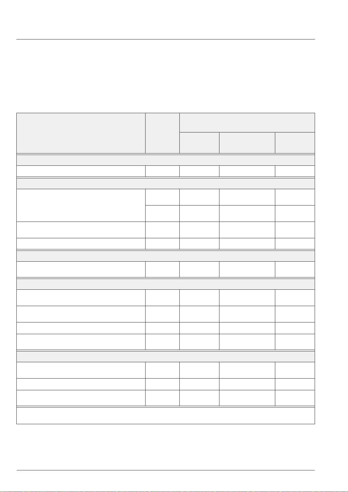
2.6.2. Examples
Table 2–1 shows some examples of how these modes
can be used to configure the IC. The list is not
intended to be complete, more modes are possible.
Table 2–1: Examples of Surround Configurations
Configurations
Stereo
Stereo
Surround Modes as defined by Dolby Laboratories
Dolby Surround Pro Logic
Dolby 3 Stereo
Virtual Dolby Surround
Surround Modes that use the Dolby Adaptive Matrix
3-Channel Virtual Surround
Passive Matrix Surround Sound
Speaker
Config-
1)
uration
(L,R) −− −
2)
(L,C,R,S) ADAPTIVE REAR_
(L,R,S) ADAPTIVE REAR_
(L,C,R) ADAPTIVE FRONT_
(L,R) ADAPTIVE 3D_PANORAMA PHANTOM
2)
(L,C,R) ADAPTIVE 3D_PANORAMA NORMAL
Surround Processing Mode
Register (4B
Decoder Matrix
[15:8]
hex
)
Surround
Reproduction
[7:4]
SPEAKER
SPEAKER
SPEAKER
Center Mode
[3:0]
NORMAL
WIDE
PHANTOM
NORMAL
WIDE
WIDE
4-Channel Surround
3-Channel Surround
2-Channel Micronas 3D Surround Sound (MSS)
3-Channel Micronas 3D Surround Sound (MSS)
(L,C,R,S) PASSIVE REAR_
SPEAKER
(L,R,S) PASSIVE REAR_
SPEAKER
(L,R) PASSIVE 3D_PANORAMA OFF
(L,C,R) PASSIVE 3D_PANORAMA NORMAL
NORMAL
WIDE
OFF
WIDE
Special Effects Surround Sound
4-Channel Surround for mono
2-Channel Virtual Surround for mono
3-Channel Virtual Surround for mono
1)
Speakers not in use are muted automatically.
2)
The implementation in products requires a license from Dolby Laboratories Licensing Corporation (see note on page 3).
(L,C,R,S) EFFECT REAR_
SPEAKER
(L,R) EFFECT 3D_PANORAMA OFF
(L,C,R) EFFECT 3D_PANORAMA NORMAL
NORMAL
WIDE
WIDE
10 Micronas
Page 11

PRELIMINARY DATA SHEET DPL 4519G
2.6.3. Application Tips for using 3D-PANORAMA
2.6.3.1. Sweet Spot
Good results are on ly obtained in a rather close area
along the middle axis between the two loudspeakers:
the sweet spot. Moving away from this position
degrades the effect.
2.6.3.2. Clipping
For the test at Dolby Labs, it is very impor tant to h ave
no clipping effects even with worst case signals. The
2
S-prescale register has to be set to values of max
I
(16
10
hex
). This is sufficient in terms of clipping.
dec
However, it was found, that by reducing the prescale to
a value lower than 16
more convincing effects are
dec
generated in case of very high dynamic signals. A
value of 10
is a good compromise between overall
dec
volume and additional headroom.
Test signals : sine sweep with 0 dB FS; L only, R only,
L&R equal phase, L&R anti phase.
Listening tests: Dolby Trailers (train trailer, city trailer,
canyon trailer...)
Great care has to be taken with sys tems that us e one
common subwoofer: A single loudspeaker cannot
reproduce vir tual sound locations. The cros sove r frequency must be lower than 120 Hz.
2.6.3.4. Cabinet Requirements
During listeni ng tests at Dolby Laboratories, no resonances in the cabinet should occur.
Good material to check for resonances are the Dolby
Trailers or other dynamic sound tracks.
2.6.4. Input and Output Levels for
Dolby Surround Pro Logic
2
The nominal inpu t level (in put sensitivity) for the I
Inputs is −15 dBFS. The highest possible input level of
0 dBFS is a ccepted with out inter nal overflow. The I
S-
2
S-
prescale value should be set to values of max 0 dB
).
(16
dec
With higher prescale values lower input sensitivities
can be accommodated. A higher input sensitivity is not
possible, because at least 15 dB headr oo m is requ ired
for every input according to the Dolby specifications.
2.6.3.3. Loudspeaker Requirements
The loudspeakers used and their positioning inside the
TV set will greatly influence the performance of the virtualizer. The algorithm works with the direct sound
path. Reflected sound waves reduce the effect. So it’s
most important to have as much direct sound as possible, compared to indirect sound.
To obtain the approval for a TV set, Dolby Laboratories
require mounting the loudspeakers at the front of t he
set. Loudspeakers radiat ing to the side of the TV set
will not produce co nvincing effects. Good d irect ional ity
of the loudspeakers towards the listener is optimal.
The virt ualizer was specially developed for implementation in TV sets. Even for rather small stereo TV's, sufficient sound effects can be obtained. For small set s,
the loudspeaker placement should be to the side of the
CRT; for large screen sets (or 16:9 sets), mounting the
loudspeakers below the CRT is a ccep table (larg e separation is preferred, low frequency sp eakers shoul d be
outmost to avoid cancellation effects). Using externa l
loudspeakers with a la rge stereo base will not create
optimal effects.
A full-scale left only i nput (0 dBFS ) will produce a full scale left only output (at 0 dB volume). The typical output level is 1.37 Vrms for DACM_L. The same holds
true for right only signa ls (1.37 Vrms for DACM_R). A
full-scale inp ut level on both inputs (Lin=Rin=0 dBFS)
will give a center only output with maximum level. A
full-scale input level on both inputs (but Lin and Rin
with inverted phases) will give a surround-only signal
with maximum level.
For reproducing Dolby Pro Logic according to its specifications, the center and surround outputs must be
amplified by 3 dB with respect to th e L and R output
signals. This can be done in two ways:
1. By implementing 3 dB more amplification for center
and surround loudspeaker outputs.
2. By always selecting volume for L and R 3 dB lower
than center and surround. Method 1 is preferable,
as method 2 lowers the achievable SNR for left and
right signals by 3 dB.
2.7. SCART Signal Routing
2.7.1. SCART Out Select
The loudspeakers should be able to reproduce a wi de
frequency range. The most impor tant fr equency range
starts from 160 Hz and ranges up to 5 kHz.
The SCART Output Select block includes full matrix
switching facilities. The switches are controlled by the
ACB user register (see page page 30).
Micronas 11
Page 12

DPL 4519G PRELIMINARY DATA SHEET
2.7.2. Stand-by Mode
If the DPL 4519G is switched off by first pulling
STANDBYQ low and th en ( aft er >1 µs delay) switching
off DVSUP and AVSUP, but k eeping AHVSUP (‘Stand-
by’-mode), the SCART switches maintain their position and function. This allows the copying from
selected SCART-inputs to SCART-outputs in the TV
set’s stand-by mode.
In case of power on or starting from stand-by (see
details on the power-up sequence in Fig. 4–19 on
page 52), all internal registers except the ACB register
(page 30) are reset to the default configuration (see
Table 3–5 on page 17) . The reset positio n of the ACB
register becomes ac ti ve after the fi rst I
2
C transmission
into the Baseband Processing part (subaddress
). By transmitting the ACB regis ter firs t, the rese t
12
hex
state can be redefined.
2
S Bus Interfaces
2.8. I
The DPL 451 9G has two kin ds of interfaces: synch ron
master/slave input/output interfaces running on 48 kHz
and an asynchron slave interface.
The interfaces accept a variety of formats with different
sample width, bit-orientation, and wordstrobe timing.
2
S options are set by means of the MODUS or
All I
2
S_CONFIG register.
I
2
2.8.1. Synchronous I
The synchronous I
S-Interface(s)
2
S bus interface consists of the
pins:
– I2S_DA_IN1, I2S_DA_IN2/3 (I2S_DA_IN2 in
PQFP80 package):
2
S serial data input, 16, 18...32 bits per sample.
I
2.8.2. Asynchronous I
The asynchronous I
2
S-Interface
2
S slave interface allows the
reception of digi tal audio s ignals with arbitrar y sample
rates from 5 to 50 kHz. The synchronization is performed by means of an adaptive sample rate converter. No oversampling clock is required.
The following pins are us ed for the asynchronous I
2
bus interface (serve only as input):
– I2S_WS3
– I2S_CL3
– I2S_DA_IN2/3 (I2S_DA_IN3 in PQFP80 package).
2
The interface accepts I
S-input streams with MS B first
and with sample widths of 16,18...32 bits. With left/
right alignment and wordstrobe timing polarity, there
are additional paramete rs available for the adaption to
a variety of formats i n the I2S CONF IGURATION register.
2
2.8.3. Multichannel I
S-Output
Bit[0:1] of the I2S CONFIGURATION register (see
page 20) switches the output to 8 channel multichannel output mode. The bit res olution per channel is 32
bit in master mode. While the first two channels can be
selected on the source s elect matr ix, chann els 3- 8 are
always connected to the I2S_3 input channels 3-8.
Both, master and slave mode is possible, as long as as
the wordstrobe has only one positive edge per frame in
slave mode.
2
2.8.4. Asynchronous Multichannel I
S-Input
The DPL 4519 G supports two kinds of asynchronous
multichannel input:
S
–I2S_DA_OUT:
2
S serial data output, 16, 18...32 bits per sample.
I
– I2S_CL:
2
S serial clock.
I
–I2S_WS:
2
S word strobe signal defines the left and right
I
sample.
If the DPL 4519G serves as the master on the I
2
interface, the clock and word strobe lines are driven by
S
– the asynchronous I2S_3 interface can be switched
to multichannel mode (bit [8] of the I2S CONFIGURATION register is set to 1. The number of channels must be even and less or equal eight.
– All I2S input lines (I2S_DA_IN1, I2S_DA_IN2 and
I2S_DA_IN3 in PQFP80 package) can be switched
to asynchronous two channel mode (bit[2] set to 1 in
the I2S CONFIGURATION register). The common
clock is I2S_WS3 and I2S_CL3. No synchronous
I2S interfaces are available in this mode.
the DPL 4519G. In this mode, only 16, 32 bits per
sample can be selected. In slave mode, these lines are
input to the DPL 4519G and the DPL 4519G clock is
synchronized to 384 times the I2S_WS rate (48 kHz).
2
S timing diagram is shown in Fig. 4–21 on
An I
page 55.
12 Micronas
Page 13

PRELIMINARY DATA SHEET DPL 4519G
2.9. Digital Control I/O Pins
The static level of the digital input/output pins
D_CTR_I/O_0/1 is switchable between HIGH and
LOW via the I
(see page 30). This enables the contro lling o f externa l
hardware switch es or other devices via I
2
C-bus by means of the ACB register
2
C-bus.
The Modus Register can set the digital input/output
pins to high impedance (see page 19). So the pins can
be used as input. The current state can be read out of
the STATUS register (see page page 21).
2.10. Clock PLL Oscillator and Crystal Specifications
The DPL 4519G derives all internal system clocks
from the 18.432 MHz oscillator. In I
2
S-slave mode of
the synchronous interface, the clock is phase-locked to
the corresponding source.
For proper performance, the DPL clock oscillator
requires a 18.432-MHz crystal. Note that for the
phase-locked modes (I
tolerance are required. The asynchronous I
2
S-slave), crystals with tighter
2
S3 slave
interface uses a different locking mechanism and does
not require tighter crystal tolerances.
Micronas 13
Page 14
DPL 4519G PRELIMINARY DATA SHEET
3. Control Interface
2
C Bus Interface
3.1. I
3.1.1. Device and Subaddresses
2
The DPL 4519G is controlled via the I
C bus slave
interface.
The IC is selected by transmitting one of the
DPL 4519G device addres ses. In order to allow up to
three DPL or MSP ICs to be connected to a single bus,
an address select pin (ADR_SEL) has been implemented. With ADR_SEL pulled to high, low, or left
open, the DPL 4519G responds to different device
addresses. A device addr ess pair is defi ned as a wr it e
address and a read address (see Table 3–1).
Writing is done by sending the device write address,
followed by the subaddress byte, two address bytes,
and two data bytes. Reading is done by sending the
write device addres s, followed by the subaddress byte
and two address bytes. Wit hout sendin g a stop c ondition, reading of the addressed data is completed by
sending the device read address and reading two
bytes of data. Refer to Sectio n 3.1.4. for the I
protocol and to Section 3.4. “Programming Tips” on
page 34 for proposals of DPL 4519G I
2
2
C bus
C telegrams.
See Table 3–2 for a list of available subaddresses.
typical respons e time is a bout 0.3 ms. If the DPL cannot accept another complete byte of data until it has
performed some other function (for example, serv icing
an internal in terrupt), it wi ll hold the clock line I2C_ CL
LOW to force the transmitter into a wait state. The
positions within a transmissio n wher e thi s may happen
are indicated by “Wait” in S ec tio n 3.1.4. The ma xi mum
wait period of the DPL dur ing normal operation mode
is less than 1 ms.
3.1.2. Internal Hardware Error Handling
In case of any internal hardware error (e.g. interruption
of the power supply of the DPL), the DP L’s wait period
is extended to 1.8 ms. After this time period elapses,
the DPL releases data and clock lines.
Indicating and solving the error status:
To indicate the error status, the remaining acknowledge bits of the actual I
Additionally, bit[14] of CONTROL is set to one. The
DPL can then be reset via the I
2
C-protocol will be left high.
2
C bus by transmitting
the reset condition to CONTROL.
Indication of reset:
Besides the possib ility of ha rdware res et, the DPL can
also be reset by means of the RE SET bit in the CO NTROL register by the controller via I
Due to the interna l architec ture of the DPL 4519G, the
IC cannot react immediately to an I
2
Table 3–1: I
ADR_SEL Low
Mode Write Read Write Read Write Read
DPL device add res s 80
C Bus Device Addresses
2
C bus.
2
C request. The
(connected to DVSS)
hex
81
hex
Any reset, even caused by an unstable reset line etc.,
is indicated in bit[15] of CONTROL.
2
A general timing diagram of the I
C bus is shown in
Fig. 4–21 on page 55.
High
(connected to DVSUP)
84
hex
85
hex
88
hex
Left Open
89
Table 3–2: I2C Bus Subaddresses
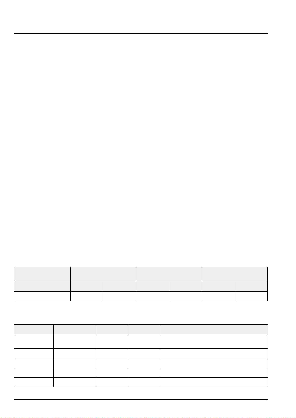
Name Binary Value Hex Value Mode Function
CONTROL 0000 0000 00 Read/Write Write: Sof tware reset of DPL (see Table 3– 3)
Read: Hardware error status of DPL
WR_DEM 0001 0000 10 Write write address demodulator
hex
RD_DEM 0001 0001 11 Write read address demodulator
WR_DSP 0001 0010 12 Write write address DSP
RD_DSP 0001 0011 13 Write read address DSP
14 Micronas
Page 15
PRELIMINARY DATA SHEET DPL 4519G
3.1.3. Description of CONTROL Register
Table 3–3: CONTROL as a Write Register
Name Subaddress Bit[15] (MSB) Bits[14:0]
CONTROL 00 hex 1 : RESET
0
0 : normal
Table 3–4: CONTROL as a Read Register (only DPL 4519G-versions from A2 on)
Name Subaddress Bit[15] (MSB) Bit[14] Bits[13:0]
CONTROL 00 hex Reset status after last reading of CONTROL:
0 : no reset occured
1 : reset occured
Reading of CONTROL will reset the bits[15,14] of CONTROL. After Power-on,
Internal hardware status:
not of interest
0 : no error occured
1 : internal error occured
bit[15] of CONTROL will be set; it must be
read once to be resetted.
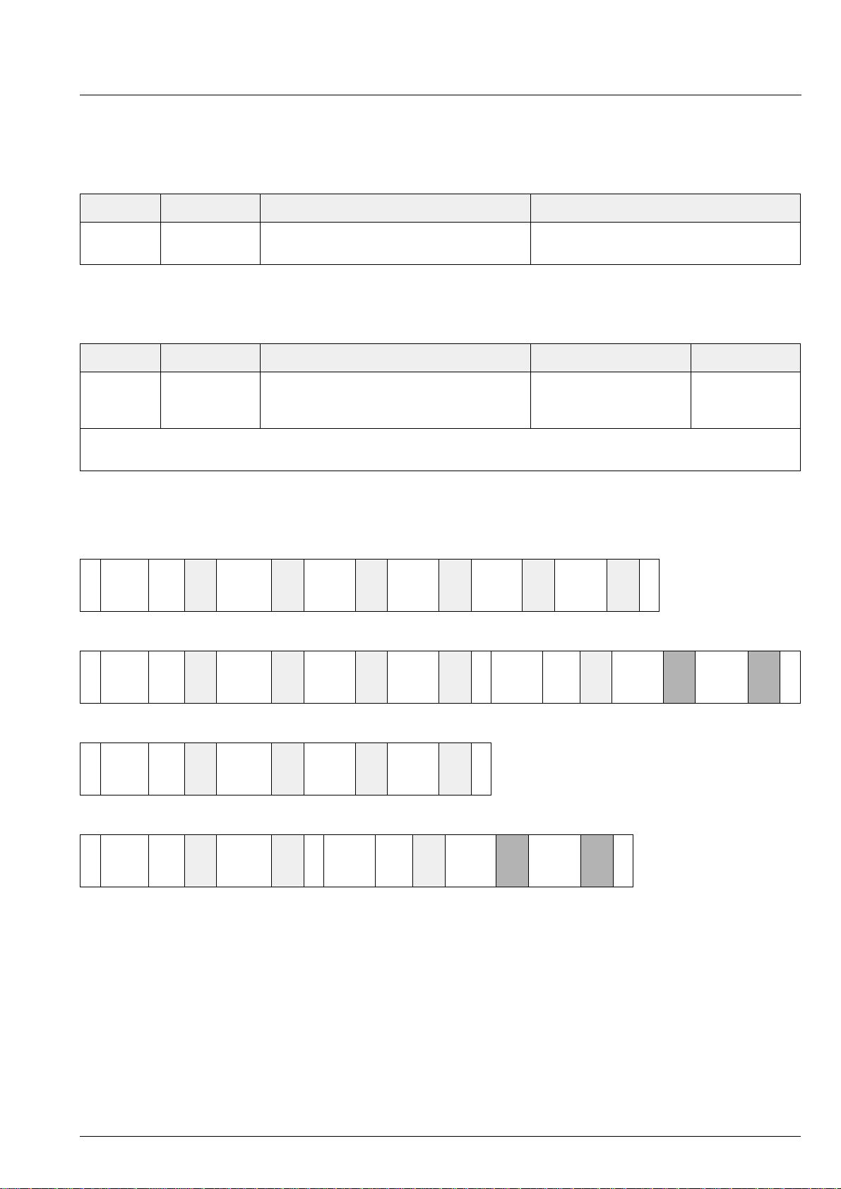
3.1.4. Protocol Description
Write to DSP
Swrite
device
address
Wait
ACK sub-addr ACK addr-byte
high
ACK addr-byte
low
ACK data-byte-
high
ACK data-byte
low
ACK P
Read from DSP
Swrite
device
address
ACK sub-addr ACK addr-byte
Wait
high
ACK addr-byte
low
ACK S read
device
address
Wait
ACK data-byte-
high
ACK data-byte
Write to Control
Swrite
device
address
ACK sub-addr ACK data-byte
Wait
high
ACK data-byte
low
ACK P
Read from Control
Swrite
device
address
Wait
Note: S = I
P = I
ACK 00hex ACK S read
2
C-Bus Start Condition from master
2
C-Bus Stop Condition from master
device
address
Wait
ACK data-byte-
high
ACK data-byte
low
NAK P
ACK = Acknowledge-Bit: LOW on I2C_DA from slave (= DPL, light gray) or master (= controller dark gray)
NAK = Not Acknowledge-Bit: HIGH on I2C_DA from master (dark gray) to indicate ‘End of Read’
or from DPL indicating internal error state
2
Wait = I
C-Clock line is held low, while the DPL is processing the I2C command.
This waiting time is max. 1 ms
NAK P
low
Micronas 15
Page 16

DPL 4519G PRELIMINARY DATA SHEET
I2C_DA
1
0
S P
I2C_CL
Fig. 3–1: I2C bus protocol (MSB first; data must be stable while clock is high)
3.1.5. Proposals for General DPL 4519G
2
C Telegrams
I
3.1.5.1. Symbols
3.2. Start-Up Sequence:
Po wer-Up and I
After POWER ON or RESET (see Fi g. 4–21), the IC is
in an inactive state. All register s are in the reset pos i-
daw write device address (80
dar read device address (81
< Start Condition
hex
hex
, 85
hex
hex
or 88
or 89
hex
hex
)
)
tion, the analog out puts are muted. Th e controller has
to initialize all r egisters for which a non-default setting
is necessary.
, 84
> Stop Cond iti on
aa Address Byte
dd Data Byte
3.3. DPL 4519G Programming Interface
2
C Controlling
3.1.5.2. Write Telegrams
<daw 00 d0 00> write to CONTROL register
<daw 10 aa aa dd dd> write data into demodulator
<daw 12 aa aa dd dd> write data into DSP
3.1.5.3. Read Telegrams
<daw 00 <dar dd dd> read data from
CONTROL register
<daw 11 aa aa <dar dd dd> read data from demodulator
<daw 13 aa aa <dar dd dd> read data from DSP
3.1.5.4. Examples
<80 00 80 00> RESET DPL statically
<80 00 00 00> Clear RESET
<80 12 00 08 08 20> Set Main channel
source to I2S3 - L/R
<80 12 00 00 73 00> Set Main volume to 0 dB
More examples of typical application protocols are
listed in Section 3 .4. “P rogrammi ng Tips” on page 34.
3.3.1. User Registers Overview
The DPL 451 9G is controlled by mean s of user registers. The complete list of all user registers is given in
the following tables. The registers ar e partitioned into
two sections:
1. Subaddress 10
2. Subaddress 12
for writing, 11
hex
for writing, 13
hex
Write and read regis ters are 16-bit wide, whereby the
MSB is denoted bit[15]. Transmissions via I
for reading and
hex
for reading.
hex
2
C bus
have to take place in 16-bit words (two byte transfers,
with the most significant byte transferred first). All write
registers, except MODUS and I2S CONFIGURATION,
are readable.
Unused parts of the 16-bit write registers must be zero.
Addresses not given in this table must not be
accessed.
16 Micronas
Page 17
PRELIMINARY DATA SHEET DPL 4519G
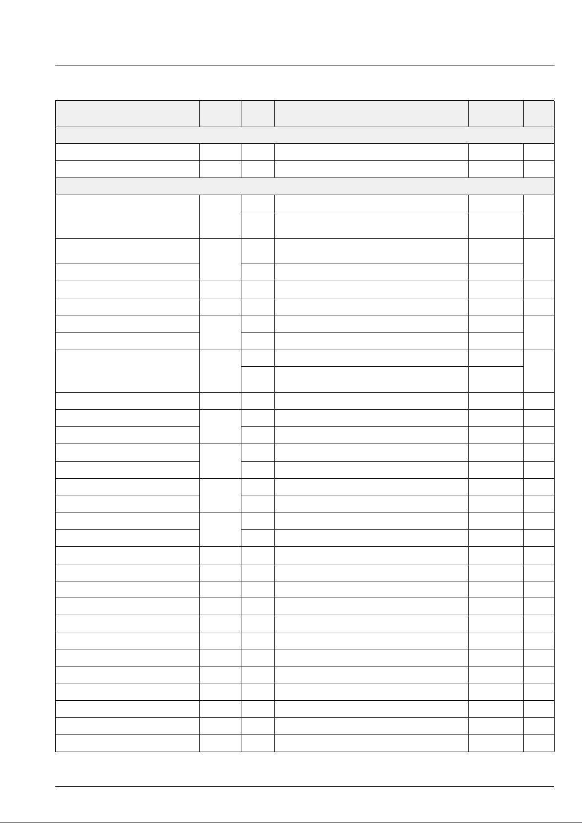
Table 3–5: List of DPL 4519G Write Registers
Write Register Address
(hex)
I2C Subaddress = 10
; Registers are
hex
not
MODUS 00 30 [15:0] I
I2S CONFIGURATION 00 40 [15:0] Configuration of I
I2C Subaddress = 12
; Registers are
hex
all
readable by using I2C Subaddress = 13
Bits Description and Adjustable Range Reset See
readable
2
S options, D_CTR_I/O modes 00 00 19
2
S format 00 00 20
hex
Page
Volume Main channel 00 00 [15:8] [+12 dB ... −114dB, MUTE] MUTE 24
[7:5]
[4:0]
Balance Main channel [L/R] 00 01 [15:8] [0...100 / 100% and 100 / 0...100%]
1/8 dB Steps
must be set to 0
000
bin
00000
bin
100%/100% 25
[−127...0 / 0 and 0 / −127...0 dB]
Balance mode Main [7:0] [Linear / logarithmic mode] linear mode
Bass Main channel 00 02 [15:8] [+20 dB ... −12dB] 0 dB 26
Treble Main channel 00 03 [15:8] [+15 dB ... −12dB] 0 dB 27
Loudness Main channel 00 04 [15:8] [0 dB ... +17 dB] 0 dB 28
Loudness filter characteristic [7:0] [NORMAL, SUPER_BASS] NORMAL
Volume A ux channel 00 06 [15:8] [+12 dB ... −114dB, MUTE] MUTE 24
[7:5]
[4:0]
1/8 dB Steps
must be set to 0
000
bin
00000
bin
Volume SCAR T1 output channel 00 07 [15:8] [+12 dB ... −114dB, MUTE] MUTE 29
2
Main source select 00 08 [15:8] [I
S1, I2S2, I2S3 ch1&2, I2S3 ch3&4,...] undefined 23
Main channel matrix [7:0] [SOUNDA, SOUNDB, STEREO, MONO] SOUNDA 23
2
Aux source select 00 09 [15:8] [I
S1, I2S2, I2S3 ch1&2, I2S3 ch3&4,...] undefined 23
Aux channel matrix [7:0] [SOUNDA, SOUNDB, STEREO, MONO] SOUNDA 23
2
SCART1 source select 00 0A [15:8] [I
S1, I2S2, I2S3 ch1&2, I2S3 ch3&4,...] undefined 23
SCART1 channel matrix [7:0] [SOUNDA, SOUNDB, STEREO, MONO] SOUNDA 23
2
S source select 00 0B [15:8] [I2S1, I2S2, I2S3 ch1&2, I2S3 ch3&4,...] undefined 23
I
2
S channel matrix [7:0] [SOUNDA, SOUNDB, STEREO, MONO] SOUNDA 23
I
2
Prescale I
Prescale I
S3 00 11 [15:8] [00
2
S2 00 12 [15:8] [00
ACB: SCART Switches a. D_CTR_I/O 00 13 [15:0] Bits [15:0] 00
Beeper 00 14 [15:0] [00
2
Prescale I
S1 00 16 [15:8] [00
hex
hex
hex
hex
... 7F
... 7F
... 7F
... 7F
]10
hex
]10
hex
]/[00
hex
hex
... 7F
hex
]10
] 00/00
hex
hex
hex
hex
hex
hex
21
21
30
30
21
Mode tone control 00 20 [15:8] [BASS/TREBLE, EQUALIZER] BASS/TREB 26
Equalizer Main ch. band 1 00 21 [15:8] [+12 dB ... −12 dB] 0 dB 27
Equalizer Main ch. band 2 00 22 [15:8] [+12 dB ... −12 dB] 0 dB 27
Equalizer Main ch. band 3 00 23 [15:8] [+12 dB ... −12 dB] 0 dB 27
Equalizer Main ch. band 4 00 24 [15:8] [+12 dB ... −12 dB] 0 dB 27
Equalizer Main ch. band 5 00 25 [15:8] [+12 dB ... −12 dB] 0 dB 27
Subwoofer level adjust 00 2C [15:8] [0 dB ... −30 dB, mute] 0 dB 29
Micronas 17
Page 18
DPL 4519G PRELIMINARY DATA SHEET
Table 3–5: List of DPL 4519G Write Registers, continued
Write Register Address
(hex)
Balance Aux channel [L/R] 00 30 [15:8] [0...100 / 100% and 100 / 0...100%]
Bits Description and Adjustable Range Reset See
Page
100 %/100 % 25
[−127...0 / 0 and 0 / −127...0 dB]
Balance mode Aux [7:0] [Linear mode / logarithmic mode] linear mode
Bass Aux channel 00 31 [15:8] [+20 dB ... −12 dB ] 0 dB 26
Treble Aux channel 00 32 [15:8] [+15 dB ... −12 dB] 0dB 27
Loudness Aux channel 00 33 [15:8] [0 dB ... +17 dB] 0 dB 28
Loudness filter characteristic [7:0] [NORMAL, SUPER_BASS] NORMAL
2
S3 Resorting 00 36 [15:8] through, straight eight, l/r eight, l/r six, l/r four,
I
2ch through
2
Surround source select 00 48 [15:8] [I
S1, I2S2, I2S3 ch1&2, I2S3 ch3&4,...] undefined 23
00
hex
22
Surround channel matrix [7:0] [SOUNDA, SOUNDB, STEREO, MONO] SOUNDA 23
Spatial effect for surround processing 00 49 [15:8] [0% - 100%] 00
Virtual surround effect strength 00 4A [15:8] [0% - 100%] 00
Decoder matrix 00 4B [15:8] [ADAPTIVE/PASSIVE/EFFECT] 00
Surround reproduction [7:4] [REAR_SPEAKER/FRONT_SPEAKER/PANORAMA/
0
3D_PANORAMA]
Center mode [3:0] [PHANTOM/NORMAL/WIDE/OFF] 0
Surround delay 00 4C [15:0] [5...31ms] 00
Noise Generator 00 4D [15:0] [NOISEL, NOISEC, NOISER, NOISES] 00
hex
hex
hex
hex
hex
hex
hex
31
31
32
32
32
32
32
Table 3–6: List of DPL 4519G Read Registers
Read Register Address
(hex)
I2C Subaddress = 11
; Registers are
hex
not
STATUS 02 00 [15:0] M onitoring of settings e.g. D_CTR_I/O 21
I2C Subaddress = 13
; Registers are
hex
not
writable
DPL hardware version code 00 1E [15:8] [00
DPL major revision code [7:0] [00
DPL product code 00 1F [15:8] [00
DPL ROM version code [7:0] [00
Bits Description and Adjustable Range See
writable
... FF
hex
hex
hex
hex
]33
hex
... FF
]33
hex
... FF
]33
hex
... FF
]33
hex
Page
18 Micronas
Page 19

PRELIMINARY DATA SHEET DPL 4519G
3.3.2. Description of User Registers
2
3.3.2.1. Write Registers on I
C Subaddress 10
hex
Table 3–7: Write Registers on I2C Subaddress 10
Register
Function Name
Address
MODUS
00 30
hex
MODUS Register
bit[15:8] 0 undefined, must be 0
bit[7] 0/1 active/tristate state of audio clock output pin
AUD_CL_OUT
bit[6] word strobe alignment (synchronous I
0 WS changes at data word boundary
1 WS changes one clock cycle in advance
bit[5] 0/1 master/slave mode of I
bit[4] 0/1 active/tristate state of I
bit[3] state of digital output pins D_CTR_I/O_0 and _1
0 active: D_CTR_I/O_0 and _1 are output pins
(can be set by means of the ACB register)
1 tristate: D_CTR_I/O_0 and _1 are input pins
(level can be read out of STATUS[4,3])
bit[2:0] 0 undefined, must be 0
hex
2
S interface
2
S output pins
MODUS
2
S)
Micronas 19
Page 20

DPL 4519G PRELIMINARY DATA SHEET
Table 3–7: Write Registers on I
Register
Function Name
Address
I2S CONFIGURA TI ON
00 40
hex
I2S CONFIGURATION Register
1)
I2S3
bit[11] I2S data alignment (must be 0 if bit[2] = 1)
0/1 left/right aligned
bit[10] wordstrobe polarity (must be 0 if bit[2] = 1)
1 0 = right, 1 = left
0 1 = right, 0 = left
bit[9] wordstrobe alignment (asynchronous I2S_3)
0 WS changes at data word boundary
1 WS changes one clock cycle in advance
bit[8] Sample Mode
0/1 Two/Multi sample
bit[7:4] Word length of each data packet = (n−2)/2
bit[3]=0, bit[8]=1 (multi-sample input mode)
0111 16 bit
1000 18 bit
...
1111 32 bit
2
C Subaddress 10
, continued
hex
I2S_CONFIG
I2S3_ALIGN
I2S3_WS_POL
I2S3_WS_MODE
I2S3_MSAMP
I2S3_MBIT
bit[3]=0, bit[8]=0 (two-sample input mode)
xxxx 16...32 bit, 18-bit valid
bit[3]=1, bit[8]=1 (multi-sample output mode)
1111 32 bit
bit[3]=1, bit[8]=0 (two-sample output mode)
0111 16 bit
1111 32 bit
2
bit[3] I
S3 Mode
1 output (I2S3 CL/WS active)
0 input (I2S3 CL/WS tristate)
2
S1/2/3
I
2
bit[2] I
S1/2/3 Timing
1I
2
S3 timing for all I2S inputs (1/2/3)
0 default mode
2
S Out
I
bit[1:0] I2S_CL frequency and I2S_DA_OUT sample length
00 2 * 16 bit (1.536 MHz Clk)
01 2 * 32 bit (3.072 MHz Clk)
10 8 * 32 bit (12.288 MHz Clk)
1)
I2S_CL3 frequency depends on bit[8] and bits[7:4] as follows:
[8] = 0, [7:4] = 0111 f = fs*(2*16)
[8] = 0, [7:4] = else f = fs*(2*32)
[8] = 1 f = fs*(8*32)
I2S3_MODE
I2S_TIMING
20 Micronas
Page 21

PRELIMINARY DATA SHEET DPL 4519G
3.3.2.2. Read Regist ers on I2C Subaddress 11
Table 3–8: Read Registers on I2C Subaddress 11
Register
Function Name
Address
02 00
hex
STATUS Register
Contains the status of the D_CTR_I/O pins
bit[15:5] undefined
bit[4] 0/1 low/high level of digital I/O pin D_CTR_I/O_1
bit[3] 0/1 low/high level of digital I/O pin D_CTR_I/O_0
bit[2:0] undefined
3.3.2.3. Write Registers on I2C Subaddress 12
hex
hex
STATUS
hex
Table 3–9: Write Registers on I2C Subaddress 12
Register
Function Name
Address
PREPROCESSING
00 16
00 12
00 11
hex
hex
hex
I2S1 Prescale
I2S2 Prescale
I2S3 Prescale
Defines the prescale value for digital I
bit[15:8] 00
10
7F
hex
hex
hex
off
0 dB gain (recommendation)
+18 dB gain (maximum gain)
hex
2
S input signals
PRE_I2S1
PRE_I2S2
PRE_I2S3
Micronas 21
Page 22

DPL 4519G PRELIMINARY DATA SHEET
Table 3–9: Write Registers on I
Register
Function Name
Address
I2S3 RESORTING MATRIX
00 36
I2S3 Resorting Matrix
hex
(not mentioned bit combinations must not be used)
Resorting of multichannel inputs
bit[15:8]
0000
: 8 channel, “through”
hex
1,2,3,4,5,6,7,8 → 1,2,3,4,5,6,7,8
L
t,Rt
L
t,Rt,Lvirtual,Rvirtual
0001
: 8 channel, “straight eight”
hex
1,2,3,4,5,6,7,8 → 7,8,1,2,3,4,5,6
L,R,S
0002
: 8 channel, “left/right eight”, “MAS 3528E”
hex
1,2,3,4,5,6,7,8 → 4,8,1,5,2,6,3,7
L,S
0003
: 6 channel, “left/right six”
hex
1,2,3,4,5,6 → -,-,1,4,2,5,3,6
L,S
0004
: 4 channel, “left/right four”, ”External ProLogic”
hex
1,2,3,4 → -,-,1,3,4,4,2,-
L,C,R,S → --,--,L,R,S
0010
: 2 channel, “through”; “Internal ProLogic”
hex
1,2 → 1,2,+,+,+,+,+,+
L
t,Rt
“+”: channel will be replaced by internally generated signal
“XPL”: internally generated signal
2
C Subaddress 12
, continued
hex
→ Lt,Rt,--,--,--,--,--,-→ Lt,Rt,L
,C,LFE,Lt,Rt→ Lt,Rt,L,R,SL,SR,C,LFE
L,SR
,C,Lt,R,SR,LFE,Rt→ Lt,Rt,L,R,SL,SR,C,LFE
L
,C,R,SR,LFE → --,--,L,R,SL,SR,C,LFE
L
virtual,Rvirtual
,C,--
L,SR
→ Lt,Rt,LPL,RPL,SPL,SPL,CPL,SUB
I2S3_Sort
,--,--,--,--
PL
22 Micronas
Page 23

PRELIMINARY DATA SHEET DPL 4519G
Table 3–9: Write Registers on I
Register
Function Name
2
C Subaddress 12
hex
Address
SOURCE SELECT AND OUTPUT CHANNEL MATRIX
Source for:
00 08
00 09
00 0A
00 0B
00 48
hex
hex
hex
hex
hex
bit[15:8] 5 I
Main Output
Aux Output
SCART1 DA Output
2
S Output
I
Surround Proc essing
2
S1 input
2
6I
7I
8I
S2 input
2
S3 input channels 1&2 (e.g. Lt,Rt)
2
S3 input channels 3&4 (e.g. L,R)1) or
Pro Logic processed L, R
2
9I
S3 input channels 5&6 (e.g. SL,SR)1) or
Pro Logic processed S, S (both channels same signal)
2
10 I
S3 input channels 7&8 (e.g. C,SUB)1) or
Pro Logic processed C, SUB
1)
exemplary channel assignment in a Micronas digital multichannel sound sys-
tem with MAS 3528E and MSP 4450G.
, continued
SRC_MAIN
SRC_AUX
SRC_SCART1
SRC_I2S
SRC_DPL
1)
00 08
00 09
00 0A
00 0B
00 48
hex
hex
hex
hex
hex
Channel Matrix for:
Main Output
Aux Output
SCART1 DA Output
2
S Output
I
Surround Proc essing
bit[7:0] 00
10
20
30
hex
hex
hex
hex
Sound A Mono (or Left Mono)
Sound B Mono (or Right Mono)
Stereo (transparent mode)
Mono (L+R)/2
Usually the matrix modes should be set to “Stereo” (transparent).
MAT_MAIN
MAT_AUX
MAT_SCART1
MAT_I2S
MAT_DPL
Micronas 23
Page 24

DPL 4519G PRELIMINARY DATA SHEET
Table 3–9: Write Registers on I
Register
Function Name
Address
MAIN AND AUX PROCESSING
00 00
00 06
hex
hex
Volume Main
Volume Aux
bit[15:8] volume table with 1 dB step size
7F
hex
7E
hex
...
74
hex
73
hex
72
hex
...
02
hex
01
hex
00
hex
FF
hex
bit[7:5] higher resolution volume table
0 +0dB
1 +0.125 dB increase in addition to the volume table
...
7 +0.875 dB increase in addition to the volume table
2
C Subaddress 12
hex
+12 dB (maximum volume)
+11 dB
+1dB
0dB
−1dB
−113 dB
−114 dB
Mute (reset condition)
Fast Mute
, continued
VOL_MAIN
VOL_AUX
bit[4:0] not used
must be set to 0
With large scale inpu t sign als , p ositi ve volume settings may lea d t o sign al clipp ing .
The DPL 45 19G Main and Aux Volume function is divided into a d igital and an
analog section. Wi th Fas t Mute, volume is reduced to mute position by digital
volume only . Analog volume is not changed. This reduces any audible DC plops.
To tur n volume on again , the volume s tep tha t has been us ed before Fast Mute
was activated must be transmitted.
24 Micronas
Page 25

PRELIMINARY DATA SHEET DPL 4519G
Table 3–9: Write Registers on I
Register
Function Name
Address
00 01
00 30
hex
hex
Balance Main Channel
Balance Aux Channel
bit[15:8] Linear Mode
7F
hex
7E
hex
...
01
hex
00
hex
FF
hex
...
82
hex
81
hex
bit[15:8] Logarithmic Mode
7F
hex
7E
hex
...
01
hex
00
hex
FF
hex
...
81
hex
80
hex
bit[3:0] Balance Mode
0
hex
1
hex
Positive balance settings reduce the left channel without affecting the right
channel; negative settings reduce the right channel leaving the left channel
unaffected.
2
C Subaddress 12
Left muted, Right 100%
Left 0.8%, Right 100%
Left 99.2%, Right 100%
Left 100%, Right 100%
Left 100%, Right 99.2%
Left 100%, Right 0.8%
Left 100%, Right muted
Left −127 dB, Right 0 dB
Left −126 dB, Right 0 dB
Left −1 dB, Right 0 dB
Left 0 dB, Right 0 dB
Left 0 dB, Right −1dB
Left 0 dB, Right −127 dB
Left 0 dB, Right −128 dB
linear
logarithmic
, continued
hex
BAL_MAIN
BAL_AUX
Micronas 25
Page 26

DPL 4519G PRELIMINARY DATA SHEET
Table 3–9: Write Registers on I
Register
Function Name
Address
00 20
hex
Tone Control Mode Main Channel
bit[15:8] 00
FF
hex
hex
Defines whether Bass/Treble or Equalizer is activated for the Main channel.
Bass/Treble and Equalizer cannot work simultaneously. If Equalizer is used,
Bass and Treble coefficients must be set to zero and vice versa.
00 02
00 31
hex
hex
Bass Main Channel
Bass Aux Channel
bit[15:8] norm al range
60
hex
58
hex
...
08
hex
00
hex
F8
hex
...
A8
hex
A0
hex
bit[15:8] extended range
7F
hex
78
hex
70
hex
68
hex
Higher resolution is possible: an LSB step in the normal range results in a gain
step of about 1/8 dB, in the extended range about 1/4 dB.
2
C Subaddress 12
bass and treble is active
equalizer is active
+12 dB
+11 dB
+1dB
0dB
−1dB
−11 dB
−12 dB
+20 dB
+18 dB
+16 dB
+14 dB
, continued
hex
TONE_MODE
BASS_MAIN
BASS_AUX
With positive bass settings, internal clipping may occur even with overall volume
less than 0 dB. This will lead to a clipped output signal. Therefore, it is not recommended to set bass to a value that, in conjunction with volume, would result
in an overall positive gain.
26 Micronas
Page 27

PRELIMINARY DATA SHEET DPL 4519G
Table 3–9: Write Registers on I
Register
Function Name
Address
00 03
00 32
hex
hex
Treble Main Channel
Treble Aux Channel
bit[15:8] 78
70
hex
hex
...
08
hex
00
hex
F8
hex
...
A8
hex
A0
hex
Higher resolution is possible: an LSB step results in a gain step of about 1/8 dB.
With positive treble settings, internal clipping may occur even with overall vol-
ume less than 0 dB. This will lead to a clipped output signal. Therefore, it is not
recommended to set treble to a value that, in conjunction with volume, would
result in an overall positive gain.
00 21
00 22
00 23
00 24
00 25
hex
hex
hex
hex
hex
Equalizer Main Channel Band 1 (below 120 Hz)
Equalizer Main Channel Band 2 (center: 500 Hz)
Equalizer Main Channel Band 3 (center: 1.5 kHz)
Equalizer Main Channel Band 4 (center: 5 kHz)
Equalizer Main Channel Band 5 (above: 10 kHz)
bit[15:8] 60
58
hex
hex
...
08
hex
00
hex
F8
hex
...
A8
hex
A0
hex
Higher resolution is possible: an LSB step results in a gain step of about 1/8 dB.
2
C Subaddress 12
+15 dB
+14 dB
+1dB
0dB
−1dB
−11 dB
−12 dB
+12 dB
+11 dB
+1dB
0dB
−1dB
−11 dB
−12 dB
, continued
hex
TREB_MAIN
TREB_AUX
EQUAL_BAND1
EQUAL_BAND2
EQUAL_BAND3
EQUAL_BAND4
EQUAL_BAND5
With positive equalizer settings, internal clipping may occur even with overall
volume less than 0 dB. This will lead to a clipped output signal. Therefore, it is
not recommended to set equalizer bands to a value that, in conjunction with volume, would result in an overall positive gain.
Micronas 27
Page 28

DPL 4519G PRELIMINARY DATA SHEET
Table 3–9: Write Registers on I
Register
Function Name
Address
00 04
00 33
hex
hex
Loudness Main Channel
Loudness Aux Channel
bit[15:8] Loudness Gain
44
hex
40
hex
...
04
hex
00
hex
bit[7:0] Loudness Mode
00
hex
04
hex
Higher resolution of Loudness Gain is possible: An LSB step results in a gain
step of about 1/4 dB.
Loudness increases the volume of low- and high-frequency signals, while keeping the amplitude of the 1-kHz reference frequency constant. The intended loudness has to be set according to the actual volume setting. Because loudness
introduces gain, it is not recommended to set loudness to a value that, in conjunction with volume, would result in an overall positive gain.
2
C Subaddress 12
, continued
hex
+17 dB
+16 dB
+1dB
0dB
normal (constant volume at 1 kHz)
Super Bass (constant volume at 2 kHz)
LOUD_MAIN
LOUD_AUX
The corner frequency for bass amplification can be set to two different values. In
Super Bass mode, the corner frequency is sh ift ed up. The poin t of c ons tan t volume is shifted from 1 kHz to 2 kHz.
28 Micronas
Page 29

PRELIMINARY DATA SHEET DPL 4519G
Table 3–9: Write Registers on I
Register
Function Name
Address
00 2C
hex
Subwoofer Level Adjustment
bit[15:8] 00
FF
hex
hex
...
E3
hex
E2
hex
...
80
hex
SCART OUTPUT CHANNEL
00 07
hex
Volume SCART1 Output Channel
bit[15:8] volume table with 1 dB step size
7F
hex
7E
hex
...
74
hex
73
hex
72
hex
...
02
hex
01
hex
00
hex
bit[7:5] higher resolution volume table
0 +0 dB
1 +0.125 dB increase in addition to the volume table
...
7 +0.875 dB increase in addition to the volume table
2
C Subaddress 12
hex
0dB
−1dB
−29 dB
−30 dB
Mute
+12 dB (maximum volume)
+11 dB
+1dB
0dB
−1dB
−113 dB
−114 dB
Mute (reset condition)
, continued
SUBW_LEVEL
VOL_SCART1
bit[4:0] 01
hex
this must be 01
hex
Micronas 29
Page 30

DPL 4519G PRELIMINARY DATA SHEET
Table 3–9: Write Registers on I
Register
Function Name
2
C Subaddress 12
Address
SCART SWITCHES AND DIGITAL I/O PINS
00 13
hex
ACB Register
Defines the level of the digital out pu t pi ns an d th e po si ti on of th e S CA RT switches
bit[15] 0/1 low/high of digital output pin D_CTR_I/O_1
(MODUS[3]=0)
bit[14] 0/1 low/high of digital output pin D_CTR_I/O_0
(MODUS[3]=0)
bit[13:5] SCART1 Output Select
xx00xx x0x SCART3 input to SCART1 output (RESET position)
xx01xx x0x SCART2 input to SCART1 output
xx10xx x0x MONO input to SCART1 output
xx11xx x0x SCART1 DA to SCART1 output
xx01xx x1x SCART1 input to SCART1 output
xx10xx x1x SCART4 input to SCART1 output
xx11xx x1x mute SCART1 output
bit[13:5] SCART2 Output Select
00xxxx 0xx SCART1 DA to SCART2 output (RESET position)
01xxxx 0xx SCART1 input to SCART2 output
10xxxx 0xx MONO input to SCART2 output
01xxxx 1xx SCART2 input to SCART2 output
10xxxx 1xx SCART3 input to SCART2 output
11xxxx 1xx SCART4 input to SCART2 output
11xxxx 0xx mute SCART2 output
, continued
hex
ACB_REG
BEEPER
00 14
hex
The RESET position bec omes active at the time of the first wr ite transmission
on the control bus to the audio pr ocessing par t. By writing to the ACB register
first, the RESET state can be redefined.
Beeper Volume and Frequency
bit[15:8] Beeper Volume
00
7F
hex
hex
off
maximum volume
bit[7:0] Beeper Frequency
01
40
FF
hex
hex
hex
16 Hz (lowest)
1kHz
4kHz
BEEPER
30 Micronas
Page 31

PRELIMINARY DATA SHEET DPL 4519G
Table 3–9: Write Registers on I
Register
Function Name
Address
SURROUND PROCESSING
00 49
hex
Spatial Effects for Surround Processing
bit[15:8] Spatial Effect Strength
7F
hex
3F
hex
...
01
hex
00
hex
bit[7:0] 00
hex
Increases the perceived basewidth of the reproduced left and right front channels. Recommended value: 50% = 40
00 4A
hex
Virtual Surround Effect Strength
bit[15:8] Virtual Surround Effect Strength
7F
hex
3F
hex
...
01
hex
00
hex
bit[7:0] 00
hex
Strength of the surround effect in PANORAMA or 3D-PANORAMA mode. In
other Surround Reproduction Modes this value must be set to 0. Recommended
value: 66% = 54
2
C Subaddress 12
Enlargement 100%
Enlargement 50%
Enlargement 1.5%
Effect off
must be 0
Effect 100%
Effect 50%
Effect 1.5%
Effect off
must be 0
.
hex
, continued
hex
.
hex
SUR_SPAT
SUR_3DEFF
Micronas 31
Page 32

DPL 4519G PRELIMINARY DATA SHEET
Table 3–9: Write Registers on I
Register
Function Name
Address
00 4B
hex
Surround Processing Mode
bit[15:8] Decoder Matrix
00
hex
10
hex
20
hex
bit[7:4] Surround Reproduction
0
hex
3
hex
5
hex
2
C Subaddress 12
, continued
hex
ADAPTIVE (for Dolby Surround Pro Logic and Virtual
Surround)
PASSIVE (for MSS, Micronas Surround Sound)
EFFECT (used for special effects and monophonic
signals)
REAR_SPEAKER: The surround signal is reproduced by
rear speakers.
FRONT_SPEAKER: The surround signal is redirected to
the front channels. There is no physical rear speaker connected.
PANORAMA: The surround signal is processed and redirected to the left and right front speakers in order to create
the illusion of a virtual rear speaker, although no physical
rear speaker is connected.
SUR_MODE
DEC_MAT
SUR_REPRO
00 4C
00 4D
hex
hex
6
hex
3D-PANORAMA: The surround signal is processed and
redirected to the left and right front speakers in order to
create the illusion of a virtual rear speaker, although no
physical rear speaker is connected.
bit[3:0] Center Mode
0
hex
1
hex
2
hex
3
hex
PHANTOM mode (no Center speaker connected)
NORMAL mode (small Center speaker)
WIDE mode (large Center speaker)
OFF mode (Center output of the Surround Decoder is
discarded. Useful only in special effect modes)
Surround Delay
bit[15:8] 05
06
hex
hex
5 ms delay in surround path (lowest)
6 ms delay in surround path
...
1F
bit[7:0] 00
hex
hex
31 ms delay in surround path (highest))
must be 0
For Dolby Surround Pro Logic designs, only 20 ms fixed or 15-30 ms variable
delay must be used. This register has no effect in 3D-PANORAMA and PANORAMA mode.
Noise Generator
bit[15:8] 00
80
bit[7:0] A0
B0
C0
D0
hex
hex
hex
hex
hex
hex
Noise generator off
Noise generator on
Noise on left channel
Noise on center channel
Noise on right channel
Noise on surround channel
Determines the active channel for the noise generator.
C_MODE
SUR_DELAY
SUR_NOISE
32 Micronas
Page 33

PRELIMINARY DATA SHEET DPL 4519G
3.3.2.4. Read Regist ers on I2C Subaddress 13
hex
Table 3–10: Read Registers on I2C Subaddress 13
Register
Function Name
Address
DPL 4519G VERSION READOUT Registers
00 1E
hex
DPL Hardware Version Code
bit[15:8] 01
hex
DPL 4519G-A1
A change in the hardware version co de defines hardware optimizations that
may have influence on the chip’s behavior. The readout of this register is ide ntical to the hardware version code in the chip’s imprint.
DPL Family Code
bit[7:4] 3
hex
DPL 4519G-A1
DPL Major Revision Code
DPL 4519G-A1
DPL 4519G - A1
00 1F
hex
bit[3:0] 7
hex
DPL Product Code
bit[15:8] 13
hex
hex
DPL_HARD
DPL_FAMILY
DPL_REVISION
DPL_PRODUCT
By means of the DPL- Product Code, the control processor i s able to decide
which TV sound standards have to be considered.
DPL ROM Version Code
bit[7:0] 41
42
hex
hex
DPL 4519G - A1
DPL 4519G - A2
A change in the ROM version code defines internal software optimizations,
that may have influence on the chip’s behavior, e.g. new features may have
been included. Whi le a soft ware change is intended t o create no compa tibility
problems, customers that want to use the new functions can identify new
DPL 4519G versions according to this number.
DPL_ROM
Micronas 33
Page 34

DPL 4519G PRELIMINARY DATA SHEET
3.4. Programming Tips
This section desc ribes the pr eferred method for initializing the DPL 4519G. The initializ ation is grouped into
four sections: analog signal pat h, input processing for
2
S, and output processing. See Fig. 2–1 on page 7 for
I
a complete signal flow.
SCART Signal Path
1. Select the source for each analog SCART output
with the ACB register.
2
S Inputs
I
2
1. Select preferred prescale for I
S inputs
(set to 0 dB after RESET).
2. Select I2S3 Resorting matrix according to the channel order of your decoding device (e.g. for
MAS 3528E chose mode 02
hex
)
Output Channels
1. Select the source channel and matrix for each output.
3.5. Examples of Minimum Initialization Codes
Initialization of the DPL 4519G according to these listings reproduces sound of the selected standard on the
Main output. All num bers are hexadecima l. The examples have the following structure:
1. Perform an I
2
C controlled reset of the IC.
2. Wr i te MO DUS regis ter
3. Set Source Selection for Main channel
(with matrix set to STEREO).
4. Set Volume Main channel to 0 dB.
3.5.1. Micronas Dolby Digital chipset
(with MAS 3528E)
<84008000>
<84000000>
<841000300020>
<8410004001F2>
<841200360002>
<8412000B0720>
<841200080820>
<841200007300>
// Softreset
// MODUS-Register: I2S slave
// I2S-config-Register
// I2S3 Resorting matrix, Mode 2
// Source Sel. I2S_out = I2S3 - Lt/R
// Source Sel. Main_out = I2S3 - L/R
// Main Volume 0 dB
t
2. Set aud io bas eba nd features
3. Select volume for each output.
34 Micronas
Page 35

PRELIMINARY DATA SHEET DPL 4519G
4. Specifications
4.1. Outline Dimensions
65
0.15±
17.2
80
0.15±
23.2
Fig. 4–1:
80-Pin Plastic Quad Flat Pack
(PQFP80)
Weight approximately 1.61 g
Dimensions in mm
3348
49
0.2±
12
64
1.75
116
1.75
0.2±
12
32
17
4164
241
0.145
1.5
0.04±
0.17
40
0.04±
0.37
25
0.05±
1.3
±0.2
3
0.055±
0.1±
0.05±
0.22
0.05±
1.4
0.1
0.1±
10
0.1±
2.7
0.1
15 x 0.5 = 7.5
0.5
10
0.1±
14
0.1±
0.5
0.1±
23 x 0.8 = 18.4
0.8
0.1±
15 x 0.5 = 7.5
20
0.1±
0.1±
0.8
15 x 0.8 = 12.0
0.1±
SPGS705000-3(P80)/1E
D0025/3E
Fig. 4–2:
64-Pin Plastic Low-Profile Quad Flat Pack
(PLQFP64)
Weight approximately 0.35 g
Dimensions in mm
Micronas 35
Page 36

DPL 4519G PRELIMINARY DATA SHEET
132
3364
57.7
±0.1
0.8
±0.2
3.8
±0.1
3.2
±0.2
1.778
1
±0.05
31 x 1.778 = 55.1
±0.1
0.48
±0.06
20.3
±0.5
0.28
±0.06
18
±0.05
19.3
±0.1
SPGS703000-1(P64)/1E
Fig. 4–3:
64-Pin Plastic Shrink Dual-Inline Package
(PSDIP64)
Weight approximately 9.0 g
Dimensions in mm
36 Micronas
Page 37

PRELIMINARY DATA SHEET DPL 4519G
4.2. Pin Connections and Short Descriptions
NC = not connected (leave vacant for future compatibility reasons)
TP = Test Pin (leave vacant - pin is used for production test only)
LV = leave vacant
X = obligatory; connect as described in application circuit diagram
AHVSS: connect to AHVSS
PQFP
80-pin
Pin No. Pin Name Type Connection
PLQFP
64-pin
PSDIP
64-pin
(if not used)
Short Description
1 64 8 NC LV Not connected
2
219I2C_CL IN/OUTX I
3 2 10 I2C_DA IN/OUT X I
4 3 11 I2S_CL IN/OUT LV I
5 4 12 I2S_WS IN/OUT LV I
6 5 13 I2S_DA_OUT OUT LV I
7 6 14 I2S_DA_IN1 IN LV I
C clock
2
C data
2
S clock
2
S word strobe
2
S data output
2
S1 data input
8 7 15 TP LV Test pin
9 8 16 TP LV Test pin
10 9 17 TP LV Test pin
11 −−DVSUP X Digital power supply +5 V
12 −−DVSUP X Digital power supply +5 V
13 10 18 DVSUP X Digital power supply +5 V
14 −−DVSS X Digital ground
15 −−DVSS X Digital ground
16 11 19 DVSS X Digital ground
2
− 12 20 I2S_DA_IN2/3 IN LV I
17 −−I2S_DA_IN2 IN LV
S2/3-data input
PQFP80: pin 22 separate I2S_DA_IN3
18 13 21 NC LV Not connected
2
19 14 22 I2S_CL3 IN LV I
20 15 23 I2S_WS3 IN LV I
S3 clock
2
S3 word strobe
21 16 24 RESETQ IN X Power-on-reset
2
22 −−I2S_DA_IN3 IN LV I
S3-data input
23 −−NC LV Not connected
24 17 25 DACA_R OUT LV Aux out, right
25 18 26 DACA_L OUT LV Aux out, left
Micronas 37
Page 38

DPL 4519G PRELIMINARY DATA SHEET
Pin No. Pin Name Type Connection
PQFP
80-pin
26 19 27 VREF2 X Reference ground 2
27 20 28 DACM_R OUT LV Loudspeaker out, right
28 21 29 DACM_L OUT LV Loudspeaker out, left
29 22 30 NC LV Not connected
30 23 31 DACM_SUB OUT LV Subwoofer output
31 24 32 NC LV Not connected
32 −−NC LV Not connected
33 25 33 SC2_OUT_R OUT LV SCART output 2, right
34 26 34 SC2_OUT_L OUT LV SCART output 2, left
35 27 35 VREF1 X Reference ground 1
36 28 36 SC1_OUT_R OUT LV SCART output 1, right
37 29 37 SC1_OUT_L OUT LV SCART output 1, left
PLQFP
64-pin
PSDIP
64-pin
(if not used)
Short Description
38 30 38 CAPL_A X Volume capacitor AUX
39 31 39 AHVSUP X Analog power supply 8.0 V
40 32 40 CAPL_M X Volume capacitor MAIN
41 −−NC LV Not connected
42 −−NC LV Not connected
43 −−AHVSS X Analog ground
44 33 41 AHVSS X Analog ground
45 34 42 AGNDC X Analog reference voltage
46 −−NC LV Not connected
47 35 43 SC4_IN_L IN LV SCART 4 input, left
48 36 44 SC4_IN_R IN LV SCART 4 input, right
49 37 45 ASG AHVSS Analog Shield Ground
50 38 46 SC3_IN_L IN LV SCART 3 input, left
51 39 47 SC3_IN_R IN LV SCART 3 input, right
52 40 48 ASG AHVSS Analog Shield Ground
53 41 49 SC2_IN_L IN LV SCART 2 input, left
54 42 50 SC2_IN_R IN LV SCART 2 input, right
55 43 51 ASG AHVSS Analog Shield Ground
56 44 52 SC1_IN_L IN LV SCART 1 input, left
38 Micronas
Page 39

PRELIMINARY DATA SHEET DPL 4519G
PQFP
80-pin
Pin No. Pin Name Type Connection
PLQFP
64-pin
PSDIP
64-pin
(if not used)
Short Description
57 45 53 SC1_IN_R IN LV SCART 1 input, right
58 46 54 NC LV Not connected
59 −−NC LV Not connected
60 47 55 MONO_IN IN LV Mono input
61 −−AVSS X Analog ground
62 48 56 AVSS X Analog ground
63 −−NC LV Not connected
64 −−NC LV Not connected
65 −−AVSUP X Analog power supply +5V
66 49 57 AVSUP X Analog power supply +5V
67 50 58 NC LV Not connected
68 51 59 NC LV Not connected
69 52 60 NC LV Not connected
70 53 61 TESTEN IN AVSS Test pin
71 54 62 XTAL_IN IN X Crystal oscillator
72 55 63 XTAL_OUT OUT X / LV Crystal oscillator
Pin descriptions)
(See also 4.3.
73 56 64 TP LV Test pin
74 57 1 AUD_CL_OUT OUT LV Audio clock output (18.432 MHz)
- −−NC LV Not connected
75 58 2 NC LV Not connected
76 59 3 NC LV Not connected
77 60 4 D_CTR_I/O_1 IN/OUT LV D_CTR_I/O_1
78 61 5 D_CTR_I/O_0 IN/OUT LV D_CTR_I/O_0
2
79 62 6 ADR_SEL IN X I
C Bus address select
80 63 7 STANDBYQ IN X Stand-by (low-active)
Micronas 39
Page 40

DPL 4519G PRELIMINARY DATA SHEET
4.3. Pin Descriptions
Pin numbers refer to the 80-pin PQFP package
Pin 1, NC – Pin not connected.
2
Pin 2, I2C_CL – I
Via this pin, the I
C Clock Input/Output (Fig. 4–8)
2
C-bus clock signal has to be supplied. The signal can be pulled down by the DPL in
case of wait conditions.
2
Pin 3, I2C_DA – I
Via this pin, the I
C Data Input/Output (Fig. 4–8)
2
C-bus data is written to or read from
the DPL.
2
Pin 4, I2S_CL – I
Clock line for the I
driven by the DPL; in slave mode, an external I
S Clock Input/Output (Fig. 4–11)
2
S bus. In master mode, this line is
2
S clock
has to be supplied.
2
Pin 5, I2S_WS – I
(Fig. 4–11)
Word strobe line for the I
line is driven by the DPL; in slave mode, an external
2
S word strobe has to be supplied.
I
Pin 6, I2S_DA_OUT1 – I
Output of digital seria l sound data of the DPL on the
2
S bus.
I
Pin 7, I2S_DA_IN1 – I
First input of digital ser ial sound data to the DPL via
2
S bus.
the I
S Word Strobe Input/Output
2
S bus. In master mode, this
2
S Data Output (Fig. 4–7)
2
S Data Input 1 (Fig. 4–9)
Pin 8, 9, 10, TP– Test pins
Pins 11, 12, 13, DVSUP* – Digital Supply Voltage
Power supply for the digital circuitry o f the DPL. Must
be connected to a power supply.
Pins 14, 15, 16, DVSS* – Digital Ground
Ground connection for the digital circuitry of the DPL.
2
Pin 17, I2S_DA_IN2 – I
Second input of digital serial sound data to the DPL via
2
S bus. In all packages except PQFP-80-pin this
the I
pin is also connected to the asynchronous I
S Data Input 2 (Fig. 4–9)
2
S inter-
face 3.
Pins 18, NC – Pin not connected.
Pin 21, RESETQ – Reset Input (Fig. 4–9)
In the steady state, high level is required. A low level
resets the DPL 4519G.
Pin 22, I2S_DA_IN3 – I
Asynchronous input of d igital serial sound d ata to the
DPL via the I
2
S bus.
2
S Data Input 3 (Fig. 4–9)
Pins 23, NC – Pin not connected.
Pins 24, 25, DA CA_R/L – Aux Outputs (Fig. 4–16)
Output of the aux signal. A 1 nF capacitor to AHVSS
must be connected to these pins. The DC offset on
these pins depends on the selected aux volume.
Pin 26, VREF2 – Reference Ground 2
Reference analog ground. This pi n mus t be co nne cte d
separately to ground (AHVSS). VREF2 serves as a
clean ground and sho uld be used as the reference for
analog connections to the Main and AUX outputs.
Pins 27, 28, DACM_R/L – Main Outputs
(Fig. 4–16)
Output of the Main signal. A 1 nF capacitor to AHVS S
must be connected to these pins. The DC offset on
these pins depends on the selected Main volume.
Pin 29 NC – Pin not connected.
Pin 30, DACM_SUB – Subwoofer Output (Fig. 4–16)
Output of the subwoofer signal. A 1-nF capacitor to
AHVSS must be conn ected to thi s pin. Due t o the low
frequency conten t of the subwoofer output, the value
of the capacitor may be increased for better supp ression of high-frequency nois e. The DC of fse t on this pi n
depends on the selected Main volume.
Pins 31, 32 NC – Pin not connected.
Pins 33, 34, SC2_OUT_R/L – SCART2 Outputs
(Fig. 4–18)
Output of the SCART2 signal. Connections to these
pins must use a 100-Ω series resistor and are i nte nded
to be AC-coupled.
Pin 35, VREF1 – Reference Ground 1
Reference analog ground. This pi n mus t be co nne cte d
separately to ground (AHVSS). VREF1 serves as a
clean ground and sho uld be used as the reference for
analog connections to the SCART outputs.
2
Pins 19, I2S_CL3 – I
Clock line for the I
available an external I
Pins 20, I2S_WS3 – I
Word strobe line for the I
mode is available an external I
S Clock Input (Fig. 4–9)
2
S bus. Since only a slave mode is
2
S clock has to be supplied.
2
S Word Strobe Input (Fig. 4–9)
2
S bus. Since only a slave
2
S word strobe has t o
Pins 36, 37, SC1_OUT_R/L – SCART1 Outputs
(Fig. 4–18)
Output of the SCART1 signal. Connections to these
pins must use a 100-Ω series resistor and are i nte nded
to be AC-coupled.
be supplied.
40 Micronas
Page 41

PRELIMINARY DATA SHEET DPL 4519G
Pin 38, CAPL_A – Volume Capacitor Aux (Fig. 4–13)
A 10-µF capacitor to AHVSUP must be connected to
this pin. It serves as a smoothing filter for volume
changes in order to su ppress audible plops. The value
of the capacitor can be lowered to 1-µF if faster
response is requi red. The area encircled by the trace
lines should be minimized; keep traces as short as
possible. This input is sensitive for magnetic induction.
Pin 39, AHVSUP* – Ana log Power Supp ly High Voltage
Power is supplied via this pin for the analog c irc ui try of
the DPL. This pin must be con nected to the +8 V supply. (+5 V-operation is possible with restrictions in perfor man ce)
Pin 40, CAPL_M – Volume Capacitor Loudspeakers
(Fig. 4–13)
A 10-µF capacitor to AHVSUP must be connected to
this pin. It serves as a smoothing filter for volume
changes in order to su ppress audible plops. The value
of the capacitor can be lowered to 1 µF if faster
response is requi red. The area encircled by the trace
lines should be minimized; keep traces as short as
possible. This input is sensitive for magnetic induction.
Pins 41, 42, NC – Pins not connected.
Pins 43, 44, AHVSS* – Ground for Analog Power Sup-
ply High Voltage
Ground connection for the analog circuitry of the DPL.
Pin 45, AGNDC – Internal Analog Reference Voltage
This pin ser ves as the internal ground c onnection for
the analog circui tr y. It must be connected to the V REF
pins with a 3.3-µF and a 100-nF c apacitor in parallel.
This pins shows a DC level of typically 3.73 V.
Pin 46, NC – Pin not connected.
Pins 47, 48, SC4_IN_L/R – SCART4 Inputs
(Fig. 4–15)
The analog input s ignal for SCART4 is fed to this pin.
Analog input connection must be AC-coupled.
Pin 55, ASG* – Analog Shield Ground
Analog ground (AHVSS) s hould be connected to this
pin to reduce cross-coupling between SCART inputs.
Pins 56, 57 SC1_IN_L/R – SCART1 Inputs (Fig. 4–15)
The analog input sig nal for SCART1 is fed to this pin.
Analog input connection must be AC-coupled.
Pin 58, NC – Pin not connected
Pin 59, NC – Pin not connected.
Pin 60 MONO_IN – Mono Input (Fig. 4–15)
The analog mono input signal is fed to this pin AC-coupled.
Pins 61, 62, AVSS* – Analog Power Supply Voltage
Ground connect ion for the analog IF input circuitry of
the DPL.
Pins 63, 64, NC – Pins not connected.
Pins 65, 66, AVSUP* – Analog Power Supply Voltage
Power is supplied via this pin for the analog IF input circuitry of the DP L. This pin must be connected to the
+5V supply.
Pin 67, 68, 69, NC – Pin not connected.
Pin 70, TESTEN – Test Enable Pin (Fig. 4–9)
This pin enables factory test modes. For normal operation, it must be connected to ground.
Pins 71, 72 XTAL_IN, XTAL_OUT – Crystal Input and
Output Pins (Fig. 4–12)
These pins are connected to an 18.432 MHz crystal
oscillator which is d igitally tuned by integrated capac itances. An external clock can be fed into XTAL_IN
(leave XTAL_OUT vacant in this case). The audio
clock output signal AUD_CL_OUT is derived from the
oscillator. External capacitors at each crystal pin to
ground (AVSS) are required. It should be verified by
layout, that no supply current for the digital circ uitry is
flowing through the ground connection point.
Pin 49, ASG* – Analog Shield Ground
Analog ground (AHVSS) should be connected to this
pin to reduce cross-coupling between SCART inputs.
Pins 50, 51, SC3_IN_L/R – SCART3 Inputs
(Fig. 4–15)
The analog input s ignal for SCART3 is fed to this pin.
Analog input connection must be AC-coupled.
Pin 52, ASG* – Analog Shield Ground
Analog ground (AHVSS) should be connected to this
pin to reduce cross-coupling between SCART inputs.
Pins 53, 54 SC2_IN_L/R – SCART2 Inputs (Fig. 4–15)
The analog input s ignal for SCART2 is fed to this pin.
Analog input connection must be AC-coupled.
Micronas 41
Pin 73, TP – This pin is needed for factory tests. For
normal operation, it must be left vacant.
Pin 74, AUD_CL_OUT – Audio Clock Output
(Fig. 4–12)
This is the 18.432 MHz main clock output.
Pins 75, 76, NC – Pins not connected.
Pins 77, 78, D_CTR_I/O_1/0 – Digital Control Input/
Output Pins (Fig. 4–11)
General purpose input/output pins.
Page 42

DPL 4519G PRELIMINARY DATA SHEET
Pin 79, ADR_SEL – I2C Bus Address Select
(Fig. 4–10)
This pin sele cts the device address for the DPL. (see
Table 3–1 ).
Pin 80, STANDBYQ – Stand-by
In normal operat ion, this pin must b e High. If the DPL
is switched to ‘Stand-by’-mode, the SCART switches
maintain their position and function. (see
Section 2.7.2.)
* Application Note:
All ground pins sh ould be con nected to one low-resistive ground plane.
All supply pins should be connected separately with
short and low-resistive lines to the power supply.
Decoupling capacitors fr om DVS UP to DVSS, AVSUP
to AVSS, and AHVSUP to AHVSS are recommended
as closely as possible to these pins. Decoupling of
DVSUP and DVSS is most impor tant. We recommend
using more than o ne capacitor. By choosing different
values, the frequency range of acti ve decoupling ca n
be extended. In our application boards we use: 220 pF,
470 pF, 1.5 nF, and 10 µF. The cap acitor with the lowest value should be placed nearest to the pins.
The ASG pins should be conn ected as close ly as possible to the IC ground. They a re intended for leading
with the SCART signals a s sh ield lines and s hould no t
be connected to ground at the SCART-connector
again.
42 Micronas
Page 43

PRELIMINARY DATA SHEET DPL 4519G
4.4. Pin Configurations
SC2_IN_L ASG
AVSUP
AVSUP
NC
NC
NC
TESTEN
XTAL_IN
XTAL_OUT
AUD_CL_OUT
NC
NC
D_CTR_I/O_1
D_CTR_I/O_0
ADR_SEL
STANDBYQ
SC2_IN_R
ASG
SC1_IN_L
SC1_IN_R
NC
NC
MONO_IN
AVSS
AVSS
NC
NC
64 63 62 61 60 59 58 57 56 55 54 53 52 51 50 49 48 47 46 45 44 43 42 41
65
66
67
68
69
70
71
72
73
TP
74
75
76
77
78
79
80
1 2 3 4 5 6 7 8 9 101112131415161718192021222324
DPL 4519G
SC3_IN_R
SC3_IN_L
ASG
SC4_IN_R
SC4_IN_L
NC
AGNDC
AHVSS
AHVSS
NC
NC
40
39
38
37
36
35
34
33
32
31
30
29
28
27
26
25
CAPL_M
AHVSUP
CAPL_A
SC1_OUT_L
SC1_OUT_R
VREF1
SC2_OUT_L
SC2_OUT_R
NC
NC
DACM_SUB
NC
DACM_L
DACM_R
VREF2
DACA_L
NC
I2C_CL
I2C_DA
I2S_CL
I2S_WS
I2S_DA_OUT
I2S_DA_IN1
NC
NC
Fig. 4–4: 80-pin PQFP package
NC
DVSUP
DVSUP DVSUP
DACA_R
NC
I2S_DA_IN3
RESETQ
I2S_WS3
I2S_CL3
NC
I2S_DA_IN2
DVSS
DVSS
DVSS
Micronas 43
Page 44

DPL 4519G PRELIMINARY DATA SHEET
SC2_IN_L
SC2_IN_R
ASG
SC1_IN_L
SC1_IN_R
NC
MONO_IN
AVSS
48 47 46 45 44 43 42 41 40 39 38 37 36 35 34 33
49AVSUP
50NC
51NC
52NC
53TESTEN
54XTAL_IN
55XTAL_OUT
56TP
57AUD_CL_OUT
58NC
59NC
60D_CTR_I/O_1
61C_CTR_I/O_0
62ADR_SEL
63STANDBYQ
64NC
12345678910111213141516
DPL 4519G
ASG
SC3_IN_R
SC3_IN_L
ASG
SC4_IN_R
SC4_IN_L
AGNDC
AHVSS
CAPL_M32
AHVSUP31
CAPL_A30
SC1_OUT_L29
SC1_OUT_R28
VREF127
SC2_OUT_L26
SC2_OUT_R25
NC24
DACM_SUB23
NC22
DACM_L21
DACM_R20
VREF219
DACA_L18
DACA_R17
I2C_CL
I2C_DA
I2S_CL
I2S_WS
I2S_DA_OUT
I2S_DA_IN1
TP
TP
Fig. 4–5: 64-pin PLQFP package
RESETQ
I2S_WS3
I2S_CL3
NC
I2S_DA_IN2/3
DVSS
DVSUP
TP
44 Micronas
Page 45

PRELIMINARY DATA SHEET DPL 4519G
4.5. Pin Circuits
VREF2
DACM_R
DACM_L
NC
DACM_SUB
NC
1AUD_CL_OUT
2NC
3NC
4D_CTR_I/O_1
5D_CTR_I/O_0
6ADR_SEL
7STANDBYQ
8NC
9I2C_CL
10I2C_DA
11I2S_CL
12I2S_WS
13I2S_DA_OUT
14I2S_DA_IN1
15TP
16TP
17TP
18DVSUP
19DVSS
DPL 4519G
20I2S_DA_IN2/3
21NC
22I2S_CL3
23I2S_WS3
24RESETQ
25DACA_R
26DACA_L
27
28
29
30
31
32
38
37
36
35
34
33
TP64
XTAL_OUT63
XTAL_IN62
TESTEN61
NC60
NC59
NC58
AVSUP57
AVSS56
MONO_IN55
NC54
SC1_IN_R53
SC1_IN_L52
ASG51
SC2_IN_R50
SC2_IN_L49
ASG48
SC3_IN_R47
SC3_IN_L46
ASG45
SC4_IN_R44
SC4_IN_L43
AGNDC42
AHVSS41
CAPL_M40
AHVSUP39
CAPL_A
SC1_OUT_L
SC1_OUT_R
VREF1
SC2_OUT_L
SC2_OUT_R
Pin numbers refer to the PQFP80 package.
DVSUP
P
N
GND
Fig. 4–7: Output Pin 6
(I2S_DA_OUT)
N
GND
Fig. 4–8: Input/Output Pins 2 and 3
(I2C_CL, I2C_DA)
Fig. 4–9: Input Pins 7, 17, 21, 22, 70, and 80
Fig. 4–6: 64-pin PSDIP package
(I2S_DA_IN1..3, RESETQ, TESTEN, STANDBYQ)
DVSUP
23 kΩ
23 kΩ
GND
ADR_SEL
Fig. 4–10: Input Pin 79 (ADR_SEL)
Micronas 45
Page 46

DPL 4519G PRELIMINARY DATA SHEET
DVSUP
P
N
GND
3−30 pF
2.5 V
500 kΩ
3−30 pF
P
N
Gain=0.5
0...2 V
≈ 3.75 V
24 kΩ
≈ 3.75 V
40 kΩ
AHVSUP
0...1.2 mA
3.3 kΩ
Fig. 4–11: Input/Output Pins 4, 5, 77, and 78
(I2S_CL, I2S_WS, D_CTR_I/O_1, D_CTR_I/O_0)
Fig. 4–12: Output/Input Pins 71, 72, and 74
(XTALIN, XTALOUT, AUD_CL_OUT)
Fig. 4–16: Output Pins 24, 25, 27, 28 and 30
(DACA_R/L, DACM_R/L, DACM_SUB)
125 kΩ
≈ 3.75 V
Fig. 4–17: Pin 45 (AGNDC)
26 pF
120 kΩ
300 Ω
≈ 3.75 V
Fig. 4–18: Output Pins 33, 34, 36, and 37
(SC_2_OUT_R/L, SC_1_OUT_R/L)
Fig. 4–13: Capacitor Pins 38 and 40
(CAPL_A, CAPL_M)
Fig. 4–14: Input Pin 60 (MONO_IN)
Fig. 4–15: Input Pins 47, 48, 50, 51, 53, 54, 56, and 57
(SC4-1_IN_L/R)
46 Micronas
Page 47

PRELIMINARY DATA SHEET DPL 4519G
4.6. Electrical Characteristics
4.6.1. Absolute Maximum Ratings
Symbol Parameter Pin Name Min. Max. Uni t
T
A
T
V
V
V
dV
P
V
I
Idig
V
I
Iana
S
SUP1
SUP2
SUP3
SUP23
TOT
Idig
Iana
Ambient Operating Temperature − 0701)°C
Storage Temperature −−40 125 °C
First Supply Voltage AHVSUP −0.3 9.0 V
Second Supply Voltage DVSUP −0.3 6.0 V
Third Supply Voltage AVSUP −0.3 6.0 V
Voltage between AVSUP
and DVSUP
AVSUP,
DVSUP
−0.5 0.5 V
Package Power Dissi pa tio n
PSDIP64
PQFP80
PLQFP64
Input Voltage, all Digital Inputs −0.3 V
1300
1000
960
SUP2
1)
+0.3 V
mW
Input Current, all Digital Pins −−20 +20 mA
Input Voltage, all Analog Inputs SCn_IN_s,
3)
−0.3 V
SUP1
+0.3 V
MONO_IN
Input Current, all Analog Inputs SCn_IN_s,
3)
−5+5mA
MONO_IN
2)
2)
I
Oana
I
Oana
Output Current, all SCART Outputs SCn_OUT_s
Output Current, all Analog Outputs
DACp_s
3) 4), 5) 4), 5)
3) 4) 4)
except SCART Outputs
I
Cana
1)
PLQFP64: 65 °C
2)
positive value means current flowing into the circuit
3)
“n” means “1”, “2”, “3”, or “4”, “s” means “L” or “R”, “p” means “M” or “A”
4)
The analog outputs are short circuit proof with respect to First Supply Voltage and ground.
5)
Total chip power dissipation must not exceed absolute maximum rating.
Output Current, other pins
connected to capacitors
CAPL_p,
AGNDC
3)
4) 4)
Stresses beyond those listed in the “Absolut e Maximum Rat ing s” may cause permanent damage to the device. This
is a stress rating onl y. Functional operation of the device at these or any ot her c onditions beyond those indi cated in
the “Recommended O perating Conditio ns/Character istics” of thi s specification is not imp lied. Exposure to absolute
maximum ratings conditions for extended periods may affect device reliability.
Micronas 47
Page 48

DPL 4519G PRELIMINARY DATA SHEET
4.6.2. Recommended Operating Conditions (TA = 0 to 70 °C)
4.6.2.1. General Recommended Operating Conditions
Symbol Parameter Pin Name Min. Typ. Max. Unit
V
SUP1
First Supply Voltage
AHVSUP 7.6 8.0 8.7 V
(8-V Operation)
First Supply Voltage
4.75 5.0 5.25 V
(5-V Operation)
V
SUP2
V
SUP3
t
STBYQ1
Second Supply Voltage DVSUP 4.75 5.0 5.25 V
Third Supply Voltage AVSUP 4.75 5.0 5.25 V
STANDBYQ Setup Time before
Turn-off of Second Supply V oltage
STANDBYQ,
DVSUP
1 µs
4.6.2.2. Analog Input and Output Recomme ndations
Symbol Parameter Pin Name Min. Typ. Max. Unit
C
AGNDC
AGNDC-Filter-Capacitor AGNDC −20% 3.3 µF
Ceramic Capacitor in Parallel −20% 100 nF
C
inSC
DC-Decoupling Capacitor in front of
SCn_IN_s
1)
−20% 330 nF
SCART Inputs
V
inSC
V
inMONO
R
LSC
C
LSC
C
VMA
SCART Input Level 2.0 V
Input Level, Mono Input MONO_IN 2.0 V
SCART Load Resistance SCn_OUT_s
SCART Load Capacitance 6.0 nF
Main/AUX Volume Capacitor CAPL_M,
CAPL_A
C
FMA
1)
“n” means “1”, “2”, or “3”, “s” means “L” or “R”, “p” means “M” or “A”
Main/AUX Filter Capacitor DACM_s,
DACA_s
1)
RMS
RMS
1)
10 kΩ
10 µF
−10% 1 +10% nF
48 Micronas
Page 49

PRELIMINARY DATA SHEET DPL 4519G
4.6.2.3. Cryst al Recomme n datio ns
Symbol Parameter Pin Name Min. Typ. Max. Unit
General Crystal Recommendations
f
P
Crystal Parallel Resonance Fre-
18.432 MHz
quency at 12 pF Load Capacitance
R
R
C
0
C
L
Crystal Series Resista nce 8 25 Ω
Crystal Shunt (Parallel) Capacitance 6.2 7.0 pF
External Load Capacitance
1)
XTAL_IN,
XTAL_OUT
PSDIP approx. 1.5
P(L)QFP approx. 3.3
pF
pF
Crystal Recommendations for Master-Slave Applications (DPL Clock must perform synchronizati on to I
clock)
f
TOL
D
TEM
Accuracy of Adjustment −20 +20 ppm
Frequency Variation
−20 +20 ppm
versus Temperature
C
1
f
CL
Crystal Recommendations for other Applications (No synchronization to I
f
TOL
D
TEM
Motional (Dynamic) Capacitance 19 24 fF
Required Open Loop Clock
Frequency (T
= 25 °C)
amb
AUD_CL_OUT
18.431 18.433 MHz
2
S clock possible)
Accuracy of Adjustment −100 +100 ppm
Frequency Variation
−50 +50 ppm
versus Temperature
2
S
f
CL
Required Open Loop Clock
Frequency (T
= 25 °C)
amb
Amplitude Recommendation for Operation with External Clock Input (C
V
XCA
1)
External capacito rs at each crystal pin to ground are r equired. They are necessary to tun e the open-loop f re-
External Clock Amplit ude XTAL_IN 0.7 V
AUD_CL_OUT 18.429 18.435 MHz
after reset typ. 22 pF)
load
pp
quency of the internal PLL and to stabilize the frequency in closed-loop operation.
Due to different layouts , the accurate capac itor size should b e determined with the customer PCB
. The sug-
gested values (1.5...3.3 pF) are figures based on experience and should serve as “start value”.
To define the capacitor size, reset the DPL without transmitti ng any further I2C telegrams. Meas ure the fre-
quency at AUD_CL_OUT-pin. Change the capacitor size until the free running frequency matches 18.432 MHz
as closely as possible. The higher the capacity, the lower the resulting clock frequency.
Micronas 49
Page 50

DPL 4519G PRELIMINARY DATA SHEET
4.6.3. Characteristics
= 0 to 70 °C, f
at T
A
= 60 °C, f
at T
A
= Junction Temperature
T
J
CLOCK
= 18.432 MHz, V
CLOCK
= 18.432 MHz, V
SUP1
= 7.6 to 8.7 V, V
SUP1
= 8 V, V
SUP2
= 4.75 to 5.25 V for min./max. values
SUP2
= 5 V for typical values,
Main (M) = Main Channel, Aux (A) = Aux Channel
4.6.3.1. General Characteristics
Symbol Parameter Pin Nam e Min. Typ. Max. Unit Test Conditions
Supply
I
SUP1A
I
SUP2A
I
SUP3A
I
SUP1S
First Supply Current (active)
(AHVSUP = 8 V)
First Supply Current (active)
(AHVSUP = 5 V)
Second Supply Current (active)
(DVSUP = 5 V)
Third Supply Current (active) AVSUP 9 13 mA
First Supply Current
(AHVSUP = 8 V)
AHVSUP 18
12
12
8
DVSUP 70 85 mA
AHVSUP 5.6 7.7 mA Standby Mode
25
17
17
11
mA
mA
mA
mA
Volume Main and Aux 0 dB
Volume Main and
Aux -30 dB
Volume Main and Aux 0 dB
Volume Main and
Aux -30 dB
STANDBYQ = low
Clock
f
CLOCK
D
CLOCK
t
JITTER
V
xtalDC
t
Startup
V
ACLKAC
V
ACLKDC
r
outHF_ACL
First Supply Current
(AHVSUP = 5 V)
Clock Input Frequency XTAL_IN 18.432 MHz
Clock High to Low Ratio 45 55 %
Clock Jitter (Verification not
provided in Production Test)
DC-Voltage Oscillator 2.5 V
Oscillator Startup Time at
VDD Slew-rate of 1 V/µs
Audio Clock Output AC Voltage AUD_CL_OUT 1.2 1.8 V
Audio Clock Output DC Voltage 0.4 0.6 V
HF Output Resistance 140 Ω
XTAL_IN,
XTAL_OUT
3.7 5.1 mA
50 ps
0.4 2 ms
pp
SUP3
load = 40 pF
I
= 0.2 mA
max
50 Micronas
Page 51

PRELIMINARY DATA SHEET DPL 4519G
4.6.3.2. Digital Inputs, Digital Outputs
Symbol Parameter Pi n N a m e Min. Typ. Max. Unit Test Conditions
Digital Input Levels
V
DIGIL
V
DIGIH
Z
DIGI
I
DLEAK
V
DIGIL
V
DIGIH
I
ADRSEL
Digital Input Low Voltage STANDBYQ
Digital Input High Voltage 0.5 V
Input Impedance 5 pF
Digital Input Leakage Current −11µA0V < U
ADR_SEL Input Low Voltage ADR_SEL 0.2 V
ADR_SEL Input High Voltage 0. 8 V
Input Current −500 −220 µAU
Digital Output Level s
V
DCTROL
V
DCTROH
Digital Output Low Voltage D_CTR_I/O_0
Digital Output High Voltage V
D_CTR_I/O_0/1
D_CTR_I/O_1
SUP2
− 0.3
0.2 V
SUP2
SUP2
D_CTR_I/O_0/1: tri-state
SUP2
SUP2
ADR_SEL
220 500 µAU
ADR_SEL
0.4 V IDDCTR = 1 mA
V IDDCTR = −1 mA
INPUT
= DVSS
= DVSUP
< DVSUP
Micronas 51
Page 52

DPL 4519G PRELIMINARY DATA SHEET
4.6.3.3. Reset Input and Power-Up
Symbol Parameter Pin Name Min. Typ. Max. Unit Test Conditions
RESETQ Input Levels
V
V
Z
RES
I
RES
RHL
RLH
DVSUP
AVSUP
V
SUP2
Reset High-Low Transition Voltage RESETQ 0.3 0.4 V
Reset Low-High Transition Voltage 0.45 0.55 V
Input Impedance 5 pF
Input Pin Leakage Current -1 1 µA0V < U
− 10%
SUP2
SUP2
t/ms
INPUT
< DVSUP
RESETQ
0.45 ×V
0.3...0.4 ×V
Internal
Reset
SUP2
SUP2
Low-to-High
Threshold
Reset Delay
>2 ms
High
Low
High-to-Low
Threshold
t/ms
t/ms
Note: The reset should
not reach high level
before the oscillator has
started. This requires a
reset delay of >2 ms
0.3 x V
SUP2
means
1.5 Volt with
= 5.0 V
V
SUP2
Fig. 4–19: Power-up sequence
52 Micronas
Page 53

PRELIMINARY DATA SHEET DPL 4519G
4.6.3.4. I2C-Bus Characteristics
Symbol Parameter Pin Name Min. Typ. Max. Unit Test Con ditions
V
I2CIL
V
I2CIH
t
I2C1
t
I2C2
t
I2C5
t
I2C6
t
I2C3
t
I2C4
f
I2C
V
I2COL
I
I2COH
t
I2COL1
t
I2COL2
I2C-BUS Input Low Voltage I2C_CL,
I2C-BUS Input High Voltage 0.6 V
I2C START Condition Setup Time 120 ns
I2C STOP Condition Setup Time 120 ns
I2C-Data Setup Time
before Rising Edge of Clock
I2C-Data Hold Time
after Falling Edge of Clock
I2C-Clock Low Pulse Time I2C_CL 500 ns
I2C-Clock High Pulse Time 500 ns
I2C-BUS Frequency 1.0 MHz
I2C-Data Output Low Voltage I2C_CL,
I2C-Data Output
High Leakage Current
I2C-Data Output Hold Time
after Falling Edge of Clock
I2C-Data Output Setup Time
before Rising Edge of Clock
I2C_DA
55 ns
55 ns
I2C_DA
15 ns
100 ns f
0.3 V
0.4 V I
1.0 µAV
SUP2
SUP2
I2COL
I2COH
= 1 MHz
I2C
= 3 mA
= 5 V
I2C_CL
I2C_DA as input
I2C_DA as output
2
Fig. 4–20: I
C bus timing diagram
T
I2C1
T
I2C5
T
I2COL2
T
I2C4
1/F
I2C
T
T
I2C3
I2C6
T
I2COL1
T
I2C2
Micronas 53
Page 54

DPL 4519G PRELIMINARY DATA SHEET
4.6.3.5. I2S-Bus Characteristics
Symbol Parameter Pin Name Min. Typ. Max. Unit Test Conditions
V
I2SIL
V
I2SIH
Z
I2SI
I
LEAKI2S
V
I2SOL
V
I2SOH
f
I2SOWS
f
I2SOCL
R
I2S10/I2S20
Synchronous I
t
s_I2S
t
h_I2S
t
d_I2S
f
I2SWS
f
I2SCL
R
I2SCL
Asynchronous I
Input Low Voltage I2S_CL
I2S_WS
Input High Voltage 0.5 V
Input Impedance 5 pF
I2S_CL3
I2S_WS3
I2S_DA_IN1..3
Input Leakage Current −11µA0V < U
I2S Output Low Voltage I2S_CL
I2S_WS
I2S Output High Voltage V
I2S_DA_OUT
SUP2
− 0.3
0.2 V
SUP2
SUP2
0.4 V I
VI
I2SOL
I2SOH
INPUT
= 1 mA
= −1 mA
< DVSUP
I2S-Word Strobe Output Frequency I2S_WS 48.0 kHz
I2S-Clock Output Frequency I2S _CL 1.536 3.072 12.288 MHz
I2S-Clock Output High/Low-Ratio 0.9 1.0 1.1
2
S Interface
I2S Input Setup Time
before Rising Edge of Clock
I2S_DA_IN1/2
I2S_CL
12 ns for details see Fig. 4–21
2
S timing diagram (syn-
“I
chronous interface)”
I2S Input Hold Time
40 ns
after Rising Edge of Clock
I2S Output Delay Time
after Falling Edge of Clock
I2S_CL
I2S_WS
28 ns C
=30 pF
L
I2S_DA_OUT
I2S-Word Strobe Input Frequency I2S_WS 48.0 kHz
I2S-Clock Input Frequency I2S_CL 1.536 3.072 12.288 MHz
I2S-Clock Input Ratio 0.9 1.1
2
S Interface
t
s_I2S3
t
h_I2S3
f
I2S3WS
f
I2S3CL
R
I2S3CL
I2S3 Input Setup Time
before Rising Edge of Clock
I2S_CL3
I2S_WS3
4 ns for details see Fig. 4–22
I2S_DA_IN3
I2S3 Input Hold Time
40 ns
after Rising Edge of Clock
I2S3-Word Strobe Input Frequency I2S_WS3 5 50 kHz
I2S3-Clock Input Frequency I2S_CL3 3.2 MHz
I2S3-Clock Input Ratio 0.9 1.1
2
“I
S timing diagram (asyn-
chronous interface)”
54 Micronas
Page 55

PRELIMINARY DATA SHEET DPL 4519G
1/F
I2S_WS
I2S_CL
I2S_DA_IN*
MODUS[6] = 0
MODUS[6] = 1
)
R LSB L MSB
Detail A
16/32 bit left channel
I2SWS
Detail C
L LSB
R MSB
16/32 bit right channel
R LSB L LSB
I2S_DA_OUT
I2S_WS
I2S_CL
I2S_DA_IN*
I2S_DA_OUT
R LSB
L MSB
Data: MSB first, I2S synchronous master
Detail B
MODUS[6] = 0
MODUS[6] = 1
)
R LSB L MSB
Detail A
16,18...32 bit left channel
16, 18...32 bit left channel
R LSB
Detail B
L MSB
Data: MSB first, I2S synchronous slave
1/F
L LSB
I2SWS
Detail C
L LSB
L LSB
R MSB
R MSB
R MSB
16/32 bit right channel16/32 bit left channel
R LSB L LSB
R LSB L LSB
16, 18...32 bit right channel
R LSB L LSB
16, 18...32 bit right channel
Detail C
1/F
I2SCL
I2S_CL
T
s_I2S
I2S_WS as INPUT
T
d_I2S
I2S_WS as OUTPUT
Fig. 4–21: I2S timing diagram (synchronous interface)
Detail A,B
I2S_CL
1)
I2S_DA_IN
I2S_DA_OUT
T
s_I2S
T
h_I2S
Note:
1)
I2S_DA_IN can be
− I2S_DA_IN1,
− I2S_DA_IN2, or
− I2S_DA_IN2/3
T
d_I2S
Micronas 55
Page 56

DPL 4519G PRELIMINARY DATA SHEET
I2S_CL3
I2S_WS3
I2S_DA_IN3
I2S_DA_IN3
I2S_CL3
I2S_DA_IN3
I2S_WS3
Left sample (I
Left sample (I
MSB
MSB
2
S_CONFIG[10] = 0)
2
S_CONFIG[10] = 1)
T
s_I2S3
T
s_I2S3
T
h_I2S3
Left aligned (I2S_CONFIG[9] = 0)
16,18...32 Bit data & clocks allo we d
Left aligned (I
16,18...32 Bit data & clocks allowed
I2S_DA_IN3
1/F
I2S3CL
2
S_CONFIG[9] = 1)
1/F
I2S3WS
Fig. 4–22: I2S timing diagram (asynchronous interface)
Right sample (I2S_CONFIG[10] = 0)
Right sample (I
MSB
Right aligned (I2S_CONFIG[11] = 1, I2S_CONFIG[9] = 0)
LSB
2
S_CONFIG[10] = 1)
MSB
16 Bit data & 16...32 clocks allowed
LSB
4.6.3.6. Analog Baseband Inputs and Outputs, AGNDC
Symbol Parameter Pin Name Min. Typ. Max. Unit Test Conditions
Analog Ground
V
AGNDC0
AGNDC Open Circuit Voltage
AHVSUP = 8 V
AHVSUP = 5 V
R
outAGN
AGNDC Output Resistance
AHVSUP = 8 V
AHVSUP = 5 V
Analog Input Resistance
R
inSC
R
inMONO
1)
“n” means “1”, “2”, “3”, or “4”; “s” means “L” or “R”
SCART Input Resistance
= 0 to 70 °C
from T
A
MONO Input Resistance
= 0 to 70 °C
from T
A
AGNDC
SCn_IN_s
3.8
2.5
70
47
1)
25 40 58 kΩ f
12583180
120
V
V
kΩ
kΩ
MONO_IN 152435kΩ f
R
≥10 MΩ
load
3 V ≤ V
AGNDC
= 1 kHz, I = 0.05 mA
signal
= 1 kHz, I = 0.1 mA
signal
≤ 4 V
56 Micronas
Page 57

PRELIMINARY DATA SHEET DPL 4519G
Symbol Parameter Pin Name Min. Typ. Max. Unit Test Con ditions
Audio Analog-to-Digital-Converter
V
AICL
Analog Input Clipping Level for
Analog-to-Digital-Conversion
(AHVSUP=8 V)
SCn_IN_s,
MONO_IN
1)
2.00 2.25 V
RMS
f
signal
= 1 kHz
Analog Input Clipping Level for
Analog-to-Digital-Conversion
(AHVSUP=5 V)
SCART Outputs
R
outSC
dV
OUTSC
A
SCtoSC
f
rSCtoSC
V
outSC
SCART Output Resistance SCn_OUT_s
Deviation of DC-Level at SCART
Output from AGNDC Voltage
Gain from
Analog Input to SCART Output
Frequency Response from
Analog Input to SCART Output
Signal Level at SCART-Output
(AHVSUP=8 V)
Signal Level at SCART-O ut put
(AHVSUP=5 V)
Main and Aux Outputs
R
outMA
V
outDCMA
Main/Aux Output Resistance DACp_s
DC-Level at Main/Aux-Output
(AHVSUP=8 V)
SCn_IN_s,
MONO_IN
→
SCn_OUT_s
SCn_OUT_s
1)
1.13 1.51 V
1)
200
330 460
200
500
Ω
Ω
RMS
f
= 1 kHz, I = 0.1 mA,
signal
= 27°C, TA = 0 to 70°C
T
j
−70 +70 mV
1)
−1.0 +0.5 dB f
1)
−0.5 +0.5 dB with resp. to 1kHz
signal
= 1 kHz
20 Hz to 20 000 Hz
1)
1.8 1.9 2.0 V
1.17 1.27 1.37 V
2.1
2.1
3.3 4.6
5.0
1.80 2.04612.28 V
RMS
RMS
kΩ
kΩ
mV
f
= 1 kHz
signal
full scale Digital Input from
2
S
I
f
= 1 kHz, I = 0.1 mA
signal
= 27°C
T
j
= 0 to 70°C
from T
A
Volume = 0 dB
Volume = -30 dB
DC-Level at Main/Aux-Output
(AHVSUP=5 V)
V
outMA
Signal Level at Main/Aux-Output
(AHVSUP=8 V)
Signal Level at Main/Aux-Output
(AHVSUP=5 V)
1)
“n” means “1”, “2”, “3”, or “4”; “s” means “L” or “R”; “p” means “M” or “A”
1.12 1.36401.60 V
1.23 1.37 1.51 V
0.76 0.90 1.04 V
mV
RMS
RMS
Volume = 0 dB
Volume = -30 dB
f
= 1 kHz
signal
full scale Digital Input from
2
S
I
Volume = 0 dB
Micronas 57
Page 58

DPL 4519G PRELIMINARY DATA SHEET
4.6.3.7. Power Supply Rejection
Symbol Parameter Pin Name Min. Typ. Max. Unit Test Conditions
PSRR: Rejection of Noise on AHVSUP at 1 kHz
PSRR AGNDC AGNDC 80 dB
2
From Analog Input to I
S Output MONO_IN,
SCn_IN_s
1)
70 dB
From Analog Input to
SCART Output
2
S Input to SCART Output SCn_OUT_s
From I
2
S Input to Main/Aux Output DACp_s
From I
1)
“n” means “1”, “2”, “3”, or “4”; “s” means “L” or “R”; “p” means “M” or “A”
MONO_IN,
SCn_IN_s
1)
SCn_OUT_s
1)
1)
1)
70 dB
60 dB
80 dB
4.6.3.8. Analog Performance
Symbol Parameter Pin Name Min. Typ. Max. Unit Test Conditions
Specifications for AHSUP=8 V
SNR Signal-to-Noise Ratio
2
from Analog Input to I
S Output MONO _IN,
from Analog Input to
SCART Output
2
S Input to SCART Output SCn_OUT _s
from I
2
S Input to Main/Aux-Output DACp_s
from I
SCn_IN_s
MONO_IN,
SCn_IN_s
1)
1)
→
SCn_OUT_s
1)
90 93 dB Input Level = −20 dB with
resp. to V
A-weighted
AICL
20 Hz...20 kHz
93 96 dB Input Level = −20 dB,
= 1 kHz,
f
sig
1)
1)
90 93 dB
A-weighted
20 Hz...20 kHz
Volume = 0 dB
90 93 dB
, f
sig
= 1 kHz,
THD Total Harmonic Distor tion
2
from Analog Input to I
from Analog Input to
SCART Output
2
S Input to SCART Output SCn_OUT _s
from I
2
S Input to Main or Aux Out-
from I
put
1)
“n” means “1”, “2”, “3”, or “4”; “s” means “L” or “R”; “p” means “M” or “A”
S Output MONO _IN,
SCn_IN_s
MONO_IN,
SCn_IN_s
→
SCn_OUT_s
DACA_s,
DACM_s
1)
1)
1)
1)
0.01 0.03 % Input Level = −3 dBr with
, f
resp. to V
unweighted
AICL
= 1 kHz,
sig
20 Hz...20 kHz
0.01 0.03 % Input Level = −3 dBr,
= 1 kHz,
f
sig
unweighted
20 Hz...20 kHz
0.01 0.03 %
0.01 0.03 %
58 Micronas
Page 59

PRELIMINARY DATA SHEET DPL 4519G
Symbol Parameter Pin Name Min. Typ. Max. Unit Test Con ditions
Specifications for AHSUP=5 V
SNR Signal-to-Noise Ratio
2
from Analog Input to I
S Output MONO_IN,
SCn_IN_s
1)
87 90 dB Input Level = −20 dB with
, f
resp. to V
A-weighted
AICL
= 1 kHz,
sig
20 Hz ...20 kHz
from Analog Input to
SCART Output
2
S Input to SCART Output SCn_OUT_s
from I
2
S Input to Main/Aux-Output
from I
MONO_IN,
SCn_IN_s
1)
→
SCn_OUT_s
1)
DACp_s
1)
1)
for Analog Volume at 0 dB
for Analog Volume at −30 dB
THD Total Harmonic Distortion
2
from Analog Input to I
from Analog Input to
SCART Output
2
S Input to SCART Output SCn_OUT_s
from I
2
S Input to Main or Aux Out-
from I
put
1)
“n” means “1”, “2”, “3”, or “4”; “s” means “L” or “R”; “p” means “M” or “A”
S Output MONO_IN,
SCn_IN_s
MONO_IN,
SCn_IN_s
→
SCn_OUT_s
DACA_s,
DACM_s
1)
1)
1)
1)
90 93 dB Input Level = −20 dB,
= 1 kHz,
f
sig
A-weighted
20 Hz ...20 kHz
Volume = 0 dB
87 90 dB
87
75
90
80
dB
dB
0.03 0.1 % Input Level = −3 dBr with
, f
resp. to V
unweighted
AICL
= 1 kHz,
sig
20 Hz ...20 kHz
0.1 % Input Level = −3 dBr,
= 1 kHz,
f
sig
unweighted
20 Hz ...20 kHz
0.1 %
0.1 %
Micronas 59
Page 60

DPL 4519G PRELIMINARY DATA SHEET
Symbol Parameter Pin Name Min. Typ. Max. Unit Test Conditions
Crosstalk Specifications
XTALK Crosstalk Attenuation Input Level = −3 dB,
= 1 kHz, unused analog
f
sig
inputs connected to ground
by Z < 1 kΩ
between left and right channel within
SCART Input/Output pair (L→R, R→L)
SCn_IN → SCn_OUT
1)
SC1_IN or SC2_IN → I2S Output
2
SC3_IN → I
2
S Input → SCn_OUT
I
S Output
1)
between left and right channel within
Main or Aux Output pair
2
S Input → DACp
I
between SCART Input/Output pairs
1)
1)
D = disturbing program
O = observed program
D: MONO/SCn_IN → SCn_OUT
O: MONO/SCn_IN → SCn_OUT
D: MONO/SCn_IN → SCn_OUT or unsel.
O: MONO/SCn_IN → I
D: MONO/SCn_IN → SCn_OUT
2
S Input → SCn_OUT
O: I
D: MONO/SCn_IN → unselected
2
S Input → SC1_OUT
O: I
2
S Output
1)
1)
1)
80
80
80
80
dB
dB
dB
dB
75 dB
100
95
100
100
dB
dB
dB
dB
unweighted
20 Hz...20 kHz
unweighted
20 Hz...20 kHz
(unweighted
20 Hz.. .20 kHz)
same signal source on left
and right disturbing channel, effect on each
observed output channel
Crosstalk between Main and Aux Output pairs
2
S Input DSP → DACp
I
1)
XTALK Crosstalk from Main or Aux Output to SCART Output
and vice versa
D = disturbing program
O = observed program
D: MONO/SCn_IN/DSP → SCn_OUT
2
S Input → DACp
O: I
D: MONO/SCn_IN/DSP → SCn_OUT
2
S Input → DACp
O: I
D: I2S Input → DACp
O: MONO/SCn_IN → SCn_OUT
D: I2S Input → DACM
2
S Input → SCn_OUT
O: I
1)
“n” means “1”, “2”, “3”, or “4”; “s” means “L” or “R”; “p” means “M” or “A”
1)
1)
1)
1)
90 dB
80
85
95
95
dB
dB
dB
dB
(unweighted
20 Hz.. .20 kHz)
same signal source on left
and right disturbing channel, effect on each
observed output channel
(unweighted
20 Hz.. .20 kHz)
same signal source on left
and right disturbing channel, effect on each
observed output channel
SCART output load resistance 10 kΩ
SCART output load resistance 30 kΩ
60 Micronas
Page 61

PRELIMINARY DATA SHEET DPL 4519G
5. Appendix A: Application Information
5.1. Phase Relationship of Analog Outputs
The analog output signals: Main, Aux, and SCART2 all
have the same phases. The SCART1 output has opposite phase.
2
Using the I
S-outputs for other DSPs or D/A convert-
ers, care must be taken to adjust for the correct phase.
I2S_OUT1/2I2S_IN1/2/3
SCART1
SCART2
SCART3
SCART4
MONO
Fig. 5–1: Phase dia gram of the DPL 4519G
Audio
Baseband
Processing
MONO, SCART1...4
Main
Aux
SCART1-Ch.
SCART1
SCART2
SCART
Output Select
Micronas 61
Page 62

DPL 4519G PRELIMINARY DATA SHEET
5.2. Application Circuit
C s. section 4.6.2.
8V(5V)
5V
DVSS
AHVSS
AHVSS
AHVSS
5V
DVSS
330 nF
330 nF
330 nF
330 nF
330 nF
330 nF
330 nF
330 nF
330 nF
60 (55) MONO_IN
56 (52) SC1_IN_L
57 (53) SC1_IN_R
55 (51) ASG
53 (49) SC2_IN_L
54 (50) SC2_IN_R
52 (48) ASG
50 (46) SC3_IN_L
51 (47) SC3_IN_R
49 (45) ASG
47 (43) SC4_IN_L
48 (44) SC4_IN_R
80 (7) STANDBYQ
79 (6) ADR_SEL
3 (10) I2C_DA
2 (9) I2C_CL
5 (12) I2S_WS
4 (11) I2S_CL
7 (14) I2S_DA_IN1
17 (20) I2S_DA_IN2
6 (13) I2S_DA_OUT
3.3 µF100
18.432
nF
+
AGNDC (42) 45
DPL 4519G
MHz
10 µF 10 µF
CAPL_M (40) 40
XTAL_IN (62) 71
DACM_L (29) 28
XTAL_OUT (63) 72
DACM_R (28) 27
DACM_SUB (31) 30
DACA_L (26) 25
DACA_R (25) 24
SC1_OUT_L (37) 37
SC1_OUT_R (36) 36
SC2_OUT_L (34) 34
SC2_OUT_R (33) 33
D_CTR_I/O_0 (5) 78
D_CTR_I/O_1 (4) 77
AUD_CL_OUT (1) 74
TESTEN (61) 70
++
1 nF
1 µF
left
1 µF
CAPL_A (38) 38
right
1 µF
1 nF
Subwoofer
1 nF
1 µF
Center
1 µF
1 nF
Surround
1 nF
100 Ω
22 µF
+
100 Ω
22 µF
+
100 Ω
22 µF
+
100 Ω
22 µF
+
AHVSS
39 (39) AHVSUP
470
pF
1.5
nF
10
µF
(5V)
43 (41) AHVSS
AHVSS
35 (35) VREF1
26 (27) VREF2
Note:
Decoupling capacitors from
− DVSUP to DVSS,
− AVSUP to AVSS, and
− AHVSUP to AHVSS
are recommended as closely
as possible to supply pins (see
AHVSS
AHVSS
application note on page 42).
RESETQ
(from Controller, see section 4.6.3.3.)
21 (24) RESETQ
220
pF
470
pF
1.5
nF
10
µF
13 (18) DVSUP
66 (57) AVSUP
16 (19) DVSS
470
pF
1.5
nF
10
µF
5 V 5 V 8 V
62 (56) AVSS
AVSS
Note: Pin numbers refer to the PQFP 80 package, number s in brackets refer to the PSDIP64 package.
62 Micronas
Page 63

PRELIMINARY DATA SHEET DPL 4519G
Micronas 63
Page 64

DPL 4519G PRELIMINARY DATA SHEET
6. Data Sheet History
1. Preliminary data sheet: "DPL 4519G Sound Processor for Digital and Analog Surround Systems",
Oct. 31, 2000, 6251-512-1PD.
First release of the preliminary data sheet.
Micronas GmbH
Hans-Bunte-Strasse 19
D-79108 Freiburg (Germany)
P.O. Box 840
D-79008 Freiburg (Germany)
Tel. +49-761-517-0
Fax +49-761-517-2174
E-mail: docservice@micronas.com
Internet: www.micronas.com
Printed in Germany
Order No. 6251-512-1PD
All information and data contained in this data sheet are without any
commitment, are not to be considered as an offer for conclusion of a
contract, nor shall they be construed as to create any liability. Any new
issue of this data sheet invalidates previous issues. Product availability
and delivery are exclusively subject to our respective order confirmation
form; the same applies to orders based on development samples delivered. By this publication, Micronas GmbH does not assume responsibility for patent infr ingements or other right s of third parties whic h may
result from its use.
Further, Micronas GmbH reserves the right to revise this publication and
to make changes to its conte nt, at any t ime, withou t obligatio n to noti fy
any person or entity of such revisions or changes.
No part of this publication may be reproduced, photocopied, stored on a
retrieval system, or transmitted without the express written consent of
Micronas GmbH .
64 Micronas
 Loading...