

Page 1
DP8571A Timer Clock Peripheral (TCP)
General Description
The DP8571A is intended for use in microprocessor based
systems where information is required for multi-tasking, data
logging or general time of day/date information. This device
is implemented in low voltage silicon gate microCMOS technology to provide low standby power in battery back-up environments. The circuit’s architecture is such that it looks
like a contiguous block of memory or I/O ports. The address
space is organized as 2 software selectable pages of 32
bytes. This includes the Control Registers, the Clock Counters, the Alarm Compare RAM, the Timers and their data
RAM, and the Time Save RAM. Any of the RAM locations
that are not being used for their intended purpose may be
used as general purpose CMOS RAM.
Time and date are maintained from 1/100 of a second to
year and leap year in a BCD format, 12 or 24 hour modes.
Day of week, day of month and day of year counters are
provided. Time is controlled by an on-chip crystal oscillator
requiring only the addition of the crystal and two capacitors.
The choice of crystal frequency is program selectable.
Two independent multifunction 10 MHz 16-bit timers are
provided. These timers operate in four modes. Each has its
own prescaler and can select any of 7 possible clock inputs.
Thus, by programming the input clocks and the timer counter values a very wide range of timing durations can be
achieved. The range is from about 400 ns (4.915 MHz oscillator) to 65,535 seconds (18 hrs., 12 min.).
Power failure logic and control functions have been integrated on chip. This logic is used by the TCP to issue a power fail
interrupt, and lock out the mp interface. The time power fails
may be logged into RAM automatically when V
Additionally, two supply pins are provided. When V
l
VCC, internal circuitry will automatically switch from the
main supply to the battery supply. Status bits are provided
to indicate initial application of battery power, system power,
and low battery detect. (Continued)
Features
Y
Full function real time clock/calendar
Ð 12/24 hour mode timekeeping
Ð Day of week and day of years counters
Ð Four selectable oscillator frequencies
Ð Parallel resonant oscillator
Y
Two 16-bit timers
Ð 10 MHz external clock frequency
Ð Programmable multi-function output
Ð Flexible re-trigger facilities
Y
Power fail features
Ð Internal power supply switch to external battery
Ð Power Supply Bus glitch protection
Ð Automatic log of time into RAM at power failure
Y
On-chip interrupt structure
Ð Periodic, alarm, timer and power fail interrupts
Y
Up to 44 bytes of CMOS RAM
Y
INTR/MFO pins programmable High/Low and push-pull
or open drain
May 1993
l
BB
DP8571A Timer Clock Peripheral (TCP)
VCC.
BB
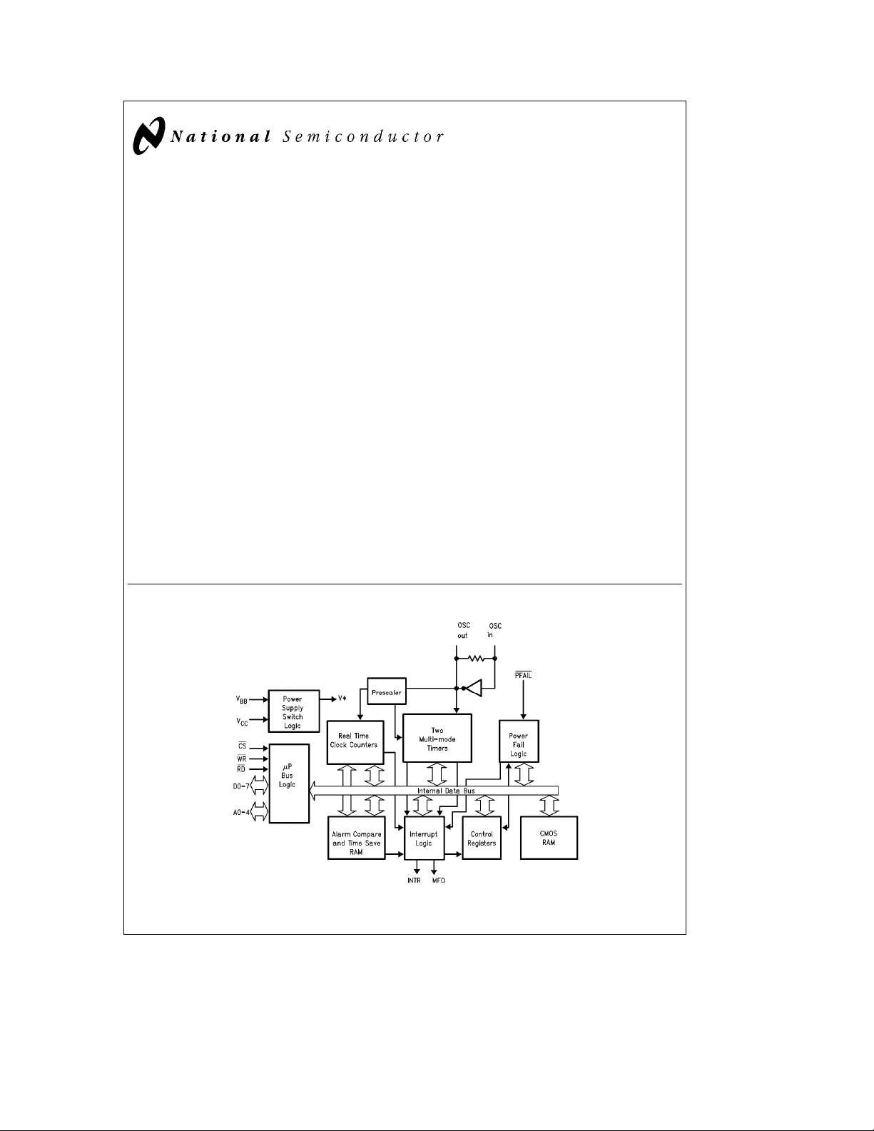
Block Diagram
FIGURE 1
TRI-STATEÉis a registered trademark of National Semiconductor Corporation.
C
1995 National Semiconductor Corporation RRD-B30M75/Printed in U. S. A.
TL/F/9979
TL/F/9979– 1
Page 2

Absolute Maximum Ratings (Notes1&2)
If Military/Aerospace specified devices are required,
please contact the National Semiconductor Sales
Office/Distributors for availability and specifications.
Supply Voltage (V
CC
)
DC Input Voltage (VIN)
DC Output Voltage (V
OUT
)
Storage Temperature Range
Power Dissipation (PD) 500 mW
Lead Temperature (Soldering, 10 sec.) 260§C
b
0.5V toa7.0V
b
0.5V to V
b
0.5V to V
b
65§Ctoa150§C
CC
CC
a
0.5V
a
0.5V
Operation Conditions
)
Socket
Socket 85
b40a
Min Max Unit
b
0.4 V
CC
0.0 V
CC
85§C
§
Supply Voltage (V
) (Note 3) 4.5 5.5 V
CC
Supply Voltage (VBB) (Note 3) 2.2 V
DC Input or Output Voltage
(V
Operation Temperature (T
IN,VOUT
)
A
Electr-Static Discharge Rating TBD 1 kV
Transistor Count 15,200
Typical Values
i
DIP Board
JA
i
PLCC Board 77§C/W
JA
DC Electrical Characteristics
V
CC
e
5Vg10%, V
BB
e
3V, V
Symbol Parameter Conditions Min Max Units
V
IH
V
IL
V
OH
V
OL
I
IN
I
OZ
I
LKG
I
CC
I
CC
I
BB
I
BLK
Note 1: Absolute Maximum Ratings are those values beyond which damage to the device may occur.
Note 2: Unless otherwise specified all voltages are referenced to ground.
Note 3: For F
2.2V min. In single Supply Mode (Power connected to V
Note 4: This parameter (V
Note 5: This specification tests I
Note 6: This specification tests I
Note 7: This specification is tested with both the timers and OSC IN driven by a signal generator. Contents of the Test Register
configured as buffered oscillator out and MFO, INTR, are configured as open drain.
Note 8: This specification is tested with both the timers off, and only OSC IN is driven by a signal generator. Contents of the Test Register
pin is not configured as buffered oscillator out.
High Level Input Voltage Any Inputs Except OSC IN, 2.0 V
(Note 4) OSC IN with External Clock V
Low Level Input Voltage All Inputs Except OSC IN 0.8 V
High Level Output Voltage I
(Excluding OSC OUT) I
Low Level Output Voltage I
(Excluding OSC OUT) I
Input Current (Except OSC IN) V
Output TRI-STATEÉCurrent V
Output High Leakage Current V
T1, MFO, INTR Pins Outputs Open Drain
Quiescent Supply Current F
(Note 7) V
Quiescent Supply Current V
(Single Supply Mode) V
(Note 7) F
Standby Mode Battery V
Supply Current OSC OUT
(Note 8) other pins
Battery, Supply Leakage 2.2VsV
e
4.194304 or 4.9152 MHz, VBBminimume2.8V. In battery backed mode, V
OSC
) is not tested on all pins at the same time.
IH
with all power fail circuitry disabled, by setting D7 of Interrupt Control Register 1 to 0.
CC
with all power fail circuitry enabled, by setting D7 of Interrupt Control Register 1 to 1.
CC
PFAIL
l
VIH,C
CC
e
100 pF (unless otherwise specified)
L
b
0.1 V
BB
OSC IN with External Clock 0.1 V
OUT
OUT
OUT
OUT
V
V
F
V
V
F
F
F
other pins at GND
V
V
pin) 4.5VsV
eb
20 mAV
eb
4.0 mA 3.5 V
e
20 mA 0.1 V
e
4.0 mA 0.25 V
e
VCCor GND
IN
e
VCCor GND
OUT
e
VCCor GND
OUT
e
32.768 kHz
OSC
e
VCCor GND (Note 5)
IN
e
VCCor GND (Note 6)
IN
e
VIHor VIL(Note 6)
IN
e
4.194304 MHz or
OSC
4.9152 MHz 8 mA
e
VCCor GND (Note 6) 20 mA
IN
e
VIHor VIL(Note 6)
IN
e
GND
BB
e
VCCor GND
IN
e
32.768 kHz 80 mA
OSC
e
4.9152 MHz or 7.5 mA
OSC
4.194304 MHz
e
GND
CC
e
open circuit,
e
GND
e
32.768 kHz 10 mA
OSC
e
4.9152 MHz or 400 mA
OSC
4.194304 MHz
s
4.0V
BB
CC
CC
e
e
CC
GND, V
5.5V, V
s
5.5V.
e
4.0V 1.5 mA
BB
e
2.2V
BB
s
b
V
BB
CC
b
0.1 V
CC
b
5 mA
0.4V. Single Supply Mode: Data retention voltage is
e
00(H), the MFO pin is not
g
1.0 mA
g
5.0 mA
g
5.0 mA
260 mA
1.0 mA
12.0 mA
e
00(H) and the MFO
V
C/W
2
Page 3
AC Electrical Characteristics
V
CC
e
5Vg10%, V
BB
e
3V, V
PFAIL
l
VIH,C
e
100 pF (unless otherwise specified)
L
Symbol Parameter Min Max Units
READ TIMING
t
AR
t
RW
t
CD
t
RAH
t
RD
t
DZ
t
RCH
t
DS
Address Valid Prior to Read Strobe 20 ns
Read Strobe Width (Note 9) 80 ns
Chip Select to Data Valid Time 80 ns
Address Hold after Read (Note 10) 3 ns
Read Strobe to Valid Data 70 ns
Read or Chip Select to TRI-STATE 60 ns
Chip Select Hold after Read Strobe 0 ns
Minimum Inactive Time between Read or Write Accesses 50 ns
WRITE TIMING
t
AW
t
WAH
t
CW
t
WW
t
DW
t
WDH
t
WCH
Address Valid before Write Strobe 20 ns
Address Hold after Write Strobe (Note 10) 3 ns
Chip Select to End of Write Strobe 90 ns
Write Strobe Width (Note 11) 80 ns
Data Valid to End of Write Strobe 50 ns
Data Hold after Write Strobe (Note 10) 3 ns
Chip Select Hold after Write Strobe 0 ns
INTERRUPT TIMING
t
ROLL
Note 9: Read Strobe width as used in the read timing table is defined as the period when both chip select and read inputs are low. Hence read commences when
both signals are low and terminates when either signal returns high.
Note 10: Hold time is guaranteed by design but not production tested. This limit is not used to calculate outgoing quality levels.
Note 11: Write Strobe width as used in the write timing table is defined as the period when both chip select and write inputs are low. Hence write commences when
both signals are low and terminates when either signal returns high.
Clock rollover to INTR out is typically 16.5 ms
AC Test Conditions
Input Pulse Levels GND to 3.0V
Input Rise and Fall Times 6 ns (10% –90%)
Input and Output
Reference Levels
TRI-STATE Reference Active High
Levels (Note 13) Active Low
Note 12: C
Note 13: S1
Capacitance (T
Note 14: This parameter is not 100% tested.
Note 15: Output rise and fall times 25 ns max (10% –90%) with 100 pF load.
e
100 pF, includes jig and scope capacitance.
L
e
VCCfor active low to high impedance measurements.
e
GND for active high to high impedance measurements.
S1
e
open for all other timing measurements.
S1
e
25§C, fe1 MHz)
A
Symbol
C
IN
C
OUT
Parameter
(Note 14)
Input Capacitance 5 pF
Output Capacitance 7 pF
1.3V
a
0.5V
b
0.5V
Typ Units
TL/F/9979– 2
3
Page 4
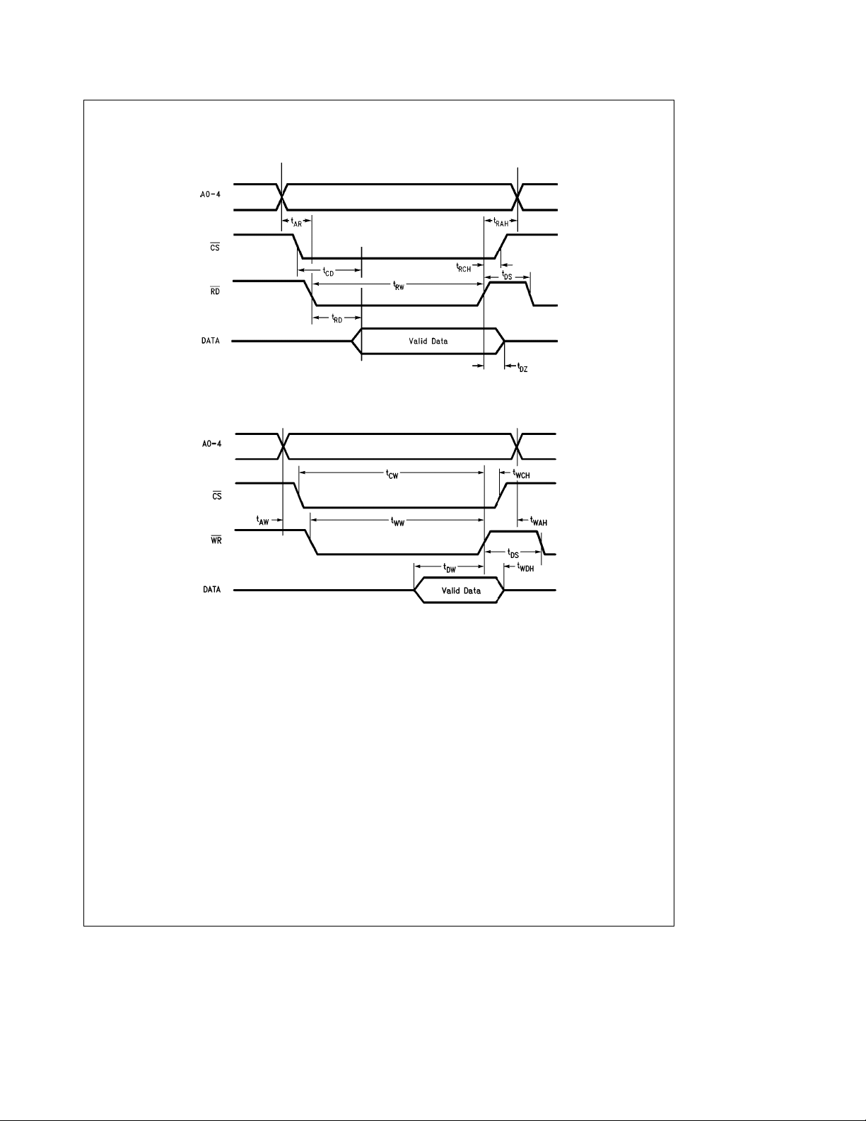
Timing Waveforms
Read Timing Diagram
TL/F/9979– 3
Write Timing Diagram
TL/F/9979– 4
4
Page 5
General Description (Continued)
The DP8571A’s interrupt structure provides four basic types
of interrupts: Periodic, Alarm/Compare, Timer, and Power
Fail. Interrupt mask and status registers enable the masking
and easy determination of each interrupt.
One dedicated general purpose interrupt output is provided.
A second interrupt output is available on the Multiple Function Output (MFO) pin. Each of these may be selected to
generate an interrupt from any source. Additionally, the
MFO pin may be programmed to be either as oscillator output or Timer 0’s output.
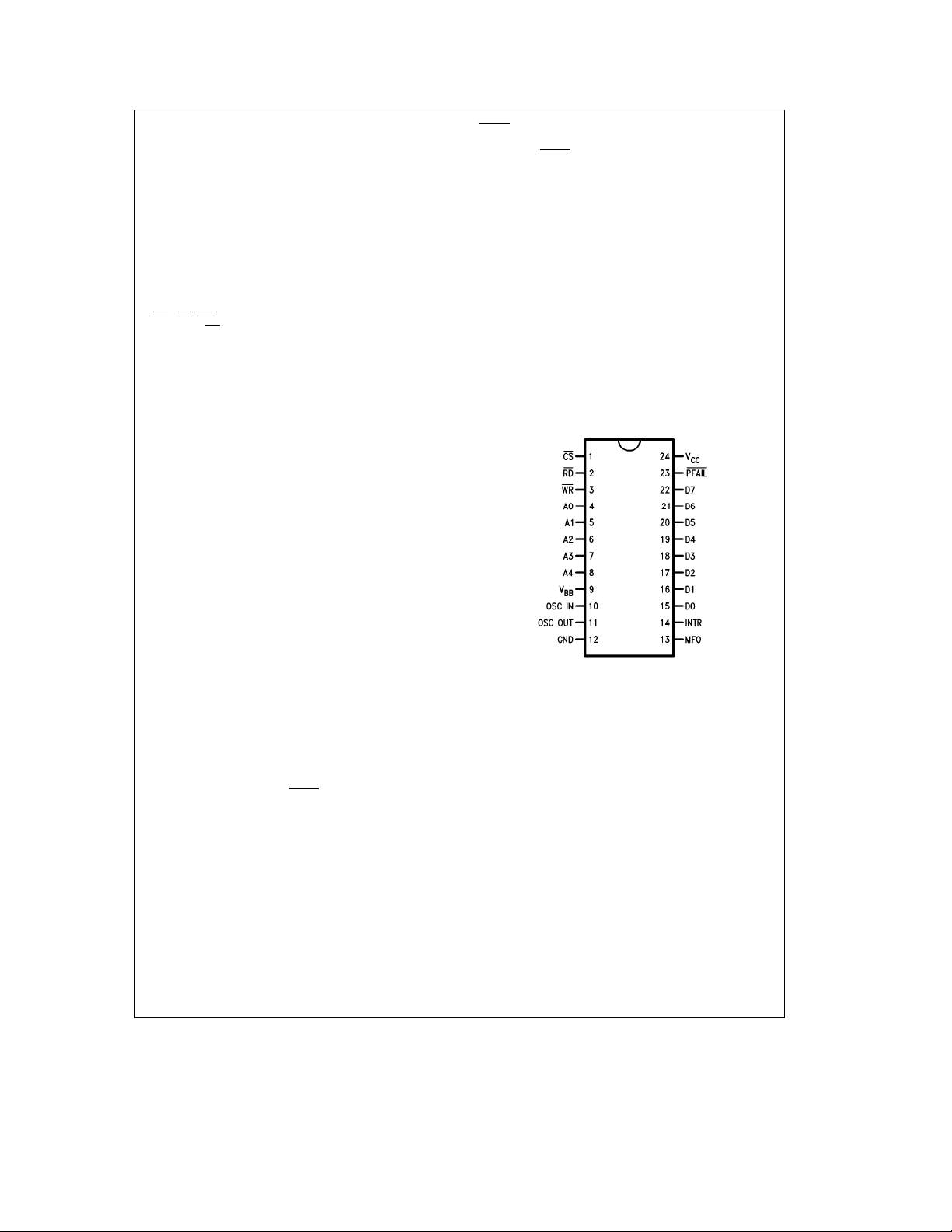
Pin Description
CS,RD,WR(Inputs): These pins interface to mP control
lines. The CS
write operations. Read and Write pins are also active low
and enable reading or writing to the TCP. All three pins are
disabled when power failure is detected. However, if a read
or write is in progress at this time, it will be allowed to complete its cycle.
A0–A4 (Inputs): These 5 pins are for register selection.
They individually control which location is to be accessed.
These inputs are disabled when power failure is detected.
OSC IN (Input): OSC OUT (Output): These two pins are
used to connect the crystal to the internal parallel resonant
oscillator. The oscillator is always running when power is
applied to V
the Real Time Mode Register have been set.
MFO (Output): The multi-function output can be used as a
second interrupt output for interrupting the mP. This pin can
also provide an output for the oscillator or the internal Timer
0. The MFO output can be programmed active high or low,
open drain or push-pull. If in battery backed mode and a
pull-up resistor is attached, it should be connected to a voltage no greater than V
during battery operation (V
INTR (Output): The interrupt output is used to interrupt the
processor when a timing event or power fail has occurred
and the respective interrupt has been enabled. The INTR
output can be programmed active high or low, push-pull or
open drain. If in battery backed mode and a pull-up resistor
is attached, it should be connected to a voltage no greater
than V
operation (V
clear the INTR, writea1totheappropriate bit(s) in the Main
Status Register.
D0–D7 (Input/Output): These 8 bidirectional pins connect
to the host mP’s data bus and are used to read from and
write to the TCP. When the PFAIL
is not in progress, these pins are at TRI-STATE.
pin is an active low enable for the read and
and VCC, and the correct crystal select bits in
BB
. This pin is configured open drain
BB
l
VCC).
BB
. This pin is configured open drain during battery
BB
l
VCC). The output is a DC voltage level. To
BB
pin goes low and a write
PFAIL
(Input): In battery backed mode, this pin can have a
digital signal applied to it via some external power detection
logic. When PFAIL
e
logic 0 the TCP goes into a lockout
mode, in a minimum of 30 ms or a maximum of 63 ms unless
lockout delay is programmed. In the single power supply
mode, this pin is not useable as an input and should be tied
to V
. Refer to section on Power Fail Functional Descrip-
CC
tion.
V
(Battery Power Pin): This pin is connected to a back-
BB
up power supply. This power supply is switched to the internal circuitry when the V
ing this pin eliminates the need for external logic to switch in
becomes lower than VBB. Utiliz-
CC
and out the back-up power supply. If this feature is not to be
used then this pin must be tied to ground, the TCP programmed for single power supply only, and power applied to
the V
pin.
CC
VCC: This is the main system power pin.
GND: This is the common ground power pin for both V
and VCC.
BB
Connection Diagram
Dual-In-Line
Top View
Order Number DP8571AN
See NS Package Number N24C
TL/F/9979– 5
5
Page 6
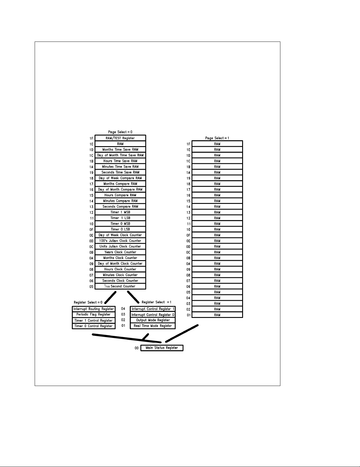
Functional Description
The DP8571A contains a fast access real time clock, two 10
MHz 16-bit timers, interrupt control logic, power fail detect
logic, and CMOS RAM. All functions of the TCP are controlled by a set of nine registers. A simplified block diagram
that shows the major functional blocks is given in
The blocks are described in the following sections:
1. Real Time Clock
2. Oscillator Prescaler
3. Interrupt Logic
4. Power Failure Logic
5. Additional Supply Management
6. Timers
Figure 1
The memory map of the TCP is shown in the memory addressing table. The memory map consists of two 31 byte
pages with a main status register that is common to both
pages. A control bit in the Main Status Register is used to
select either page.
.
Page 0 contains all the clock timer functions, while page 1
has scratch pad RAM. The control registers are split into
two separate blocks to allow page 1 to be used entirely as
scratch pad RAM. Again a control bit in the Main Status
Register is used to select either control register block.
Figure 2
shows the basic concept.
FIGURE 2. DP8571A Internal Memory Map
6
TL/F/9979– 6
Page 7
Functional Description (Continued)
INITIAL POWER-ON of BOTH V
VBBand VCCmay be applied in any sequence. In order for
the power fail circuitry to function correctly, whenever power
is off, the V
maximum of 1 MX. The user should be aware that the con-
pin must see a path to ground through a
CC
trol registers will contain random data. The first task to be
carried out in an initialization routine is to start the oscillator
by writing to the crystal select bits in the Real Time Mode
Register. If the DP8571A is configured for single supply
mode, an extra 50 mA may be consumed until the crystal
select bits are programmed. The user should also ensure
that the TCP is not in test mode (see register descriptions).
REAL TIME CLOCK FUNCTIONAL DESCRIPTION
As shown in
Figure 2
, the clock has 10 bytes of counters,
which count from 1/100 of a second to years. Each counter
counts in BCD and is synchronously clocked. The count sequence of the individual byte counters within the clock is
shown later in Table VII. Note that the day of week, day of
month, day of year, and month counters all roll over to 1.
The hours counter in 12 hour mode rolls over to 1 and the
AM/PM bit toggles when the hours rolls over to 12
e
(AM
0, PMe1). The AM/PM bit is bit D7 in the hours
counter.
All other counters roll over to 0. Also note that the day of
year counter is 12 bits long and occupies two addresses.
Upon initial application of power the counters will contain
random information.
READING THE CLOCK: VALIDATED READ
Since clocking of the counter occurs asynchronously to
reading of the counter, it is possible to read the counter
while it is being incremented (rollover). This may result in an
incorrect time reading. Thus to ensure a correct reading of
the entire contents of the clock (or that part of interest), it
must be read without a clock rollover occurring. In general
this can be done by checking a rollover bit. On this chip the
periodic interrupt status bits can serve this function. The
following program steps can be used to accomplish this.
1. Initialize program for reading clock.
2. Dummy read of periodic status bit to clear it.
3. Read counter bytes and store.
4. Read rollover bit, and test it.
5. If rollover occured go to 3.
6. If no rollover, done.
To detect the rollover, individual periodic status bits can be
polled. The periodic bit chosen should be equal to the highest frequency counter register to be read. That is if only
SECONDS through HOURS counters are read, then the
SECONDS periodic bit should be used.
READING THE CLOCK: INTERRUPT DRIVEN
Enabling the periodic interrupt mask bits cause interrupts
just as the clock rolls over. Enabling the desired update rate
and providing an interrupt service routine that executes in
less than 10 ms enables clock reading without checking for
a rollover.
READING THE CLOCK: LATCHED READ
Another method to read the clock that does not require
checking the rollover bit is to write a one into the Time
BB
and V
CC
Save Enable bit (D7) of the Interrupt Routing Register, and
then to write a zero. Writing a one into this bit will enable the
clock contents to be duplicated in the Time Save RAM.
Changing the bit from a one to a zero will freeze and store
the contents of the clock in Time Save RAM. The time then
can be read without concern for clock rollover, since internal logic takes care of synchronization of the clock. Because only the bits used by the clock counters will be
latched, the Time Save RAM should be cleared prior to use
to ensure that random data stored in the unused bits do not
confuse the host microprocessor. This bit can also provide
time save at power failure, see the Additional Supply Management Functions section. With the Time Save Enable bit
at a logical 0, the Time Save RAM may be used as RAM if
the latched read function is not necessary.
INITIALIZING AND WRITING TO THE
CALENDAR-CLOCK
Upon initial application of power to the TCP or when making
time corrections, the time must be written into the clock. To
correctly write the time to the counters, the clock would
normally be stopped by writing the Start/Stop
bit in the Real
Time Mode Register to a zero. This stops the clock from
counting and disables the carry circuitry. When initializing
the clock’s Real Time Mode Register, it is recommended
that first the various mode bits be written while maintaining
the Start/Stop
second time with the Start/Stop
bit reset, and then writing to the register a
bit set.
The above method is useful when the entire clock is being
corrected. If one location is being updated the clock need
not be stopped since this will reset the prescaler, and time
will be lost. An ideal example of this is correcting the hours
for daylight savings time. To write to the clock ‘‘on the fly’’
the best method is to wait for the 1/100 of a second periodic interrupt. Then wait an additional 16 ms, and then write
the data to the clock.
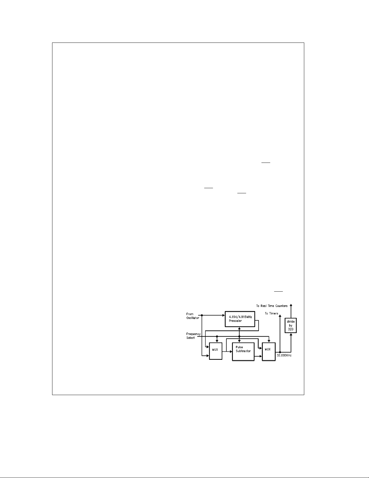
PRESCALER/OSCILLATOR FUNCTIONAL
DESCRIPTION
Feeding the counter chain is a programmable prescaler
which divides the crystal oscillator frequency to 32 kHz and
further to 100 Hz for the counter chain (see
Figure 3
). The
crystal frequency that can be selected are: 32 kHz, 32.768
kHz, 4.9152 MHz, and 4.194304 MHz.
Once 32 kHz is generated it feeds both timers and the
clock. The clock and timer prescalers can be independently
enabled by controlling the timer or clock Start/Stop
bits.
TL/F/9979– 7
FIGURE 3. Programmable Clock Prescaler Block
7
Page 8
Functional Description (Continued)
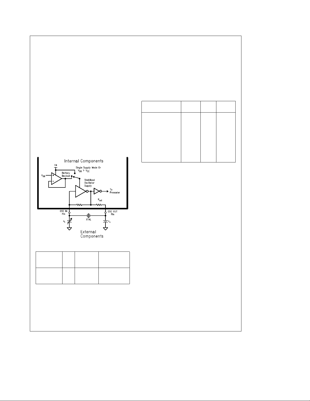
The oscillator is programmed via the Real Time Mode Register to operate at various frequencies. The crystal oscillator
is designed to offer optimum performance at each frequency. Thus, at 32.768 kHz the oscillator is configured as a low
frequency and low power oscillator. At the higher frequencies the oscillator inverter is reconfigured. In addition to the
inverter, the oscillator feedback bias resistor is included on
chip, as shown in
en from an external source if desired. Refer to test mode
application note for details. The oscillator stability is enhanced through the use of an on chip regulated power supply.
The typical range of trimmer capacitor (as shown in Oscillator Circuit Diagram
the oscillator input pin is suggested only to allow accurate
tuning of the oscillator. This range is based on a typical
printed circuit board layout and may have to be changed
depending on the parasitic capacitance of the printed circuit
board or fixture being used. In all cases, the load capaci-
tance specified by the crystal manufacturer (nominal value
11 pF for the 32.768 crystal) is what determines proper oscillation. This load capcitance is the series combination of
capacitance on each side of the crystal (with respect to
ground).
XTAL C
32/32.768 kHz 47 pF 2 pF–22 pF 150 kX to 350 kX
4.194304 MHz 68 pF 0 pF–80 pF 500X to 900X
4.9152 MHz 68 pF 29 pF–49 pF 500X to 900X
INTERRUPT LOGIC FUNCTIONAL DESCRIPTION
The TCP has the ability to coordinate processor timing activities. To enhance this, an interrupt structure has been implemented which enables several types of events to cause
interrupts. Interrupts are controlled via two Control Registers in block 1 and two Status Registers in block 0. (See
Register Description for notes on paging and also
and Table I.)
Figure 4
. The oscillator input may be driv-
Figure 4
, and in the typical application) at
FIGURE 4. Oscillator Circuit Diagram
o
C
t
(Switched
Internally)
TL/F/9979– 8
R
OUT
Figure 5
The interrupts are enabled by writing a one to the appropriate bits in Interrupt Control Register 0 and/or 1. Any of the
interrupts can be routed to either the INTR pin or the MFO
pin, depending on how the Interrupt Routing register is programmed. This, for example, enables the user to dedicate
the MFO as a non-maskable interrupt pin to the CPU for
power failure detection and enable all other interrupts to
appear on the INTR pin. The polarity for the active interrupt
can be programmed in the Output Mode Register for either
active high or low, and open drain or push pull outputs.
TABLE I. Registers that are Applicable
Register Name
Main Status Register X X 00H
Periodic Flag Register 0 0 03H
Interrupt Routing
Register
Interrupt Control
Register 0
Interrupt Control
Register 1
Output Mode
Register
The Interrupt Status Flag D0, in the Main Status Register,
indicates the state of INTR and MFO outputs. It is set when
either output becomes active and is cleared when all TCP
interrupts have been cleared and no further interrupts are
pending (i.e., both INTR and MFO are returned to their inactive state). This flag enables the TCP to be rapidly polled by
the mP to determine the source of an interrupt in a wiredÐ
OR interrupt system.
Note that the Interrupt Status Flag will only monitor the state
of the MFO output if it has been configured as an interrupt
output (see Output Mode Register description). This is true,
regardless of the state of the Interrupt Routing Register.
Thus the Interrupt Status Flag provides a true reflection of
all conditions routed to the external pins.
Status for the interrupts are provided by the Main Status
Register and the Periodic Flag Register. Bits D1 – D5 of the
Main Status Register are the main interrupt bits.
These register bits will be set when their associated timing
events occur. Enabled Alarm or Timer interrupts that occur
will set its Main Status Register bit to a one. However, an
external interrupt will only be generated if the appropriate
Alarm or Timer interrupt enable bits are set (see
Disabling the periodic bits will mask the Main Status Register periodic bit, but not the Periodic Flag Register bits. The
Power Fail Interrupt bit is set when the interrupt is enabled
and a power fail event has occurred, and is not reset until
the power is restored. If all interrupt enable bits are 0 no
interrupt will be asserted. However, status still can be read
from the Main Status Register in a polled fashion (see
ure 5
).
To clear a flag in bits D2 –D5 of the Main Status Register a 1
must be written back into the bit location that is to be
cleared. For the Periodic Flag Register reading the status
will reset all the periodic flags.
to Interrupt Control
Register Page
Select Select
0 0 04H
1 0 03H
1 0 04H
1 0 02H
Address
Figure 5
Fig-
).
8
Page 9

Functional Description (Continued)
Interrupts Fall Into Four Categories:
1. The Timer Interrupts: For description see Timer Section.
2. The Alarm Compare Interrupt: Issued when the value in
the time compared RAM equals the counter.
3. The Periodic Interrupts: These are issued at every increment of the specific clock counter signal. Thus, an interrupt is issued every minute, second, etc. Each of these
interrupts occurs at the roll-over of the specific counter.
4. The Power Fail Interrupt: Issued upon recognition of a
power fail condition by the internal sensing logic. The
power failed condition is determined by the signal on the
PFAIL
pin. The internal power fail signal is gated with the
chip select signal to ensure that the power fail interrupt
does not lock the chip out during a read or write.
ALARM COMPARE INTERRUPT DESCRIPTON
The alarm/time comparison interrupt is a special interrupt
similar to an alarm clock wake up buzzer. This interrupt is
generated when the clock time is equal to a value programmed into the alarm compare registers. Up to six bytes
can be enabled to perform alarm time comparisons on the
counter chain. These six bytes, or some subset thereof,
would be loaded with the future time at which the interrupt
will occur. Next, the appropriate bits in the Interrupt Control
Register 1 are enabled or disabled (refer to detailed description of Interrupt Control Register 1). The TCP then compares these bytes with the clock time. When all the enabled
compare registers equal the clock time an alarm interrupt is
issued, but only if the alarm compare interrupt is enabled
can the interrupt be generated externally. Each alarm compare bit in the Control Register will enable a specific byte for
comparison to the clock. Disabling a compare byte is the
same as setting its associated counter comparator to an
‘‘always equal’’ state. For example, to generate an interrupt
at 3:15 AM of every day, load the hours compare with 0 3
(BCD), the minutes compare with 1 5 (BCD) and the faster
counters with 0 0 (BCD), and then disable all other compare
registers. So every day when the time rolls over from
3:14:59.99, an interrupt is issued. This bit may be reset by
writing a one to bit D3 in the Main Status Register at any
time after the alarm has been generated.
If time comparison for an individual byte counter is disabled,
that corresponding RAM location can then be used as general purpose storage.
PERIODIC INTERRUPTS DESCRIPTION
The Periodic Flag Register contains six flags which are set
by real-time generated ‘‘ticks’’ at various time intervals, see
Figure 5
. These flags constantly sense the periodic signals
and may be used whether or not interrupts are enabled.
These flags are cleared by any read or write operation performed on this register.
To generate periodic interrupts at the desired rate, the associated Periodic Interrupt Enable bit in Interrupt Control Register 0 must be set. Any combination of periodic interrupts
may be enabled to operate simultaneously. Enabled periodic interrupts will now affect the Periodic Interrupt Flag in the
Main Status Register. The Periodic Route bit in the Interrupt
Routing Register is used to route the periodic interrupt
events to either the INTR output or the MFO output.
When a periodic event occurs, the Periodic Interrupt Flag in
the Main Status Register is set, causing an interrupt to be
generated. The mP clears both flag and interrupt by writing a
‘‘1’’ to the Periodic Interrupt Flag. The individual flags in the
periodic Interrupt Flag Register do not require clearing to
cancel the interrupt.
If all periodic interrupts are disabled and a periodic interrupt
is left pending (i.e., the Periodic Interrupt Flag is still set), the
Periodic Interrupt Flag will still be required to be cleared to
cancel the pending interrupt.
POWER FAIL INTERRUPTS DESCRIPTION
The Power Fail Status Flag in the Main Status Register
monitors the state of the internal power fail signal. This flag
may be interrogated by the mP, but it cannot be cleared; it is
cleared automatically by the TCP when system power is
restored. To generate an interrupt when the power fails, the
Power Fail Interrupt Enable bit in Interrupt Control Register
1 is set.
The Power Fail Route bit determines which output the interrupt will appear on. Although this interrupt may not be
cleared, it may be masked by clearing the Power Fail Interrupt Enable bit.
POWER FAILURE CIRCUITRY FUNCTIONAL
DESCRIPTION
Since the clock must be operated from a battery when the
main system supply has been turned off, the DP8571A provides circuitry to simplify design in battery backed systems.
This circuitry switches over to the back up supply, and isolates the DP8571A from the host system.
simplified block diagram of this circuitry, which consists of
three major sections; 1) power loss logic: 2) battery switch
over logic: and 3) isolation logic.
Detection of power loss occurs when PFAIL
bounce logic provides a 30 ms–63 ms debounce time, which
will prevent noise on the PFAIL
as a system failure. After 30 ms–63 ms the debounce logic
times out and a signal is generated indicating that system
power is marginal and is failing. The Power Fail Interrupt will
then be generated.
Figure 6
shows a
is low. De-
pin from being interpreted
9
Page 10

Functional Description (Continued)
TL/F/9979– 9
FIGURE 5. Interrupt Control Logic Overview
10
Page 11

Functional Description (Continued)
FIGURE 6. System-Battery Switchover (Upper Left), Power Fail
and Lock-Out Circuits (Lower Right)
The user may choose to have this power failed signal lockout the TCP’s data bus within 30 ms min/63 ms max or to
delay the lock-out to enable mP access after power failure is
detected. This delay is enabled by setting the delay enable
bit in the Routing Register. Also, if the lock-out delay was
not enabled the TCP will disconnect itself from the bus within 30 ms min
x
63 ms max. If chip select is low when a
power failure is detected, a safety circuit will ensure that if a
read or write is held active continuously for greater than
30 ms after the power fail signal is asserted, the lock-out will
be forced. If a lock-out delay is enabled, the DP8571A will
remain active for 480 ms after power fail is detected. This
will enable the mP to perform last minute bookkeeping before total system collapse. When the host CPU is finished
accessing the TCP it may force the bus lock-out before
480 ms has elapsed by resetting the delay enable bit.
The battery switch over circuitry is completely independent
of the PFAIL
V
BB
to operate from the V
voltage. At this time, the battery supply is switched in, VCCis
pin. A separate circuit compares VCCto the
voltage. As the main supply fails, the TCP will continue
pin until VCCfalls below the V
CC
BB
disconnected, and the device is now in the standby mode. If
indeterminate operation of the battery switch over circuit is
to be avoided, then the voltage at the V
allowed to equal the voltage at the V
BB
CC
pin.
pin must not be
TL/F/9979– 10
After the generation of a lock-out signal, and eventual
switch in of the battery supply, the pins of the TCP will be
configured as shown in Table II. Outputs that have a pull-up
resistor should be connected to a voltage no greater than
V
.
BB
TABLE II. Pin Isolation during a Power Failure
Pin
e
PFAIL
Logic 0 V
Standby Mode
l
V
BB
CC
CS,RD,WR Locked Out Locked Out
A0–A4 Locked Out Locked Out
D0–D7 Locked Out Locked Out
Oscillator Not Isolated Not Isolated
PFAIL
Not Isolated Not Isolated
INTR, MFO Not Isolated Open Drain
The Timer and Interrupt Power Fail Operation bits in the
Real-Time Mode Register determine whether or not the timers and interrupts will continue to function after a power fail
event.
As power returns to the system, the battery switch over circuit will switch back to V
greater than the battery voltage. The chip will remain in the
locked out state as long as PFAIL
power as soon as it becomes
CC
e
0. When PFAILe1
11
Page 12

Functional Description (Continued)
CC
x
BB
pin, and
the chip is unlocked, but only after another 30 ms min
63 ms max debounce time. The system designer must ensure that his system is stable when power has returned.
The power fail circuitry contains active linear circuitry that
draws supply current from V
undesirable, so this circuit can be disabled by masking the
power fail interrupt. The power fail input can perform all
lock-out functions previously mentioned, except that no external interrupt will be issued. Note that the linear power fail
circuitry is switched off automatically when using V
standby mode.
LOW BATTERY, INITIAL POWER ON DETECT, AND
POWER FAIL TIME SAVE
There are three other functions provided on the DP8571A to
ease power supply control. These are an initial Power On
detect circuit, which also can be used as a time keeping
failure detect, a low battery detect circuit, and a time save
on power failure.
On initial power up the Oscillator Fail Flag will be set to a
one and the real time clock start bit reset to a zero. This
indicates that an oscillator fail event has occurred, and time
keeping has failed.
The Oscillator Fail flag will not be reset until the real-time
clock is started. This allows the system to discriminate between an initial power-up and recovery from a power failure.
If the battery backed mode is selected, then bit D6 of the
Periodic Flag Register must be written low. This will not affect the contents of the Oscillator Fail Flag.
Another status bit is the low battery detect. This bit is set
only when the clock is operating under the V
when the battery voltage is determined to be less than 2.1V
(typical). When the power fail interrupt enable bit is low, it
disables the power fail circuit and will also shut off the low
battery voltage detection circuit as well.
To relieve CPU overhead for saving time upon power failure,
the Time Save Enable bit is provided to do this automatically. (See also Reading the Clock: Latched Read.) The Time
Save Enable bit, when set, causes the Time Save RAM to
follow the contents of the clock. This bit can be reset by
software, but if set before a power failure occurs, it will automatically be reset when the clock switches to the battery
supply (not when a power failure is detected by the PFAIL
pin). Thus, writing a one to the Time Save bit enables both a
software write or power fail write.
SINGLE POWER SUPPLY APPLICATIONS
The DP8571A can be used in a single power supply application. To achieve this, the V
ground, and the power connected to V
The Oscillator Failed/Single Supply bit in the Periodic Flag
Register should be set to a logic 1, which will disable the
oscillator battery reference circuit. The power fail interrupt
should also be disabled. This will turn off the linear power
fail detection circuits, and will eliminate any quiescent power
drawn through these circuits. Until the crystal select bits are
initialized, the DP8571A may consume about 50 mA due to
arbitrary oscillator selection at power on.
(This extra 50 mA is not consumed if the battery backed
mode is selected).
TIMER FUNCTIONAL DESCRIPTION
The DP8571A contains 2 independent multi-mode timers.
Each timer is composed of a 16-bit negative edge triggered
. In some cases this may be
CC
pin must be connected to
BB
and PFAIL pins.
CC
binary down counter and associated control. The operation
is similar to existing mP peripheral timers except that several
features have been enhanced. The timers can operate in
four modes, and in addition, the input clock frequency can
be selected from a prescaler over a wide range of frequencies. Furthermore, these timers are capable of generating
interrupts and the Timer 0 output signal is available as a
hardware output via the MFO pin. Timer 1 output, however,
is not available as a hardware output signal. Both the interrupt and MFO outputs are fully programmable active high, or
in
low, open drain, or push-pull.
Figure 7
shows the functional block diagram of one of the
timers. The timer consists of a 16-bit counter, two 8-bit input
registers, two 8-bit output registers, clock prescaler, mode
control logic, and output control logic. The timer and the
data registers are organized as two bytes for each timer.
Under normal operations a read/write to the timer locations
will read or write to the data input register. The timer contents can be read by setting the counter Read bit (RD) in the
timer control register.
TIMER INITIALIZATION
The timer’s operation is controlled by a set of registers, as
listed in Table III. These consist of 2 data input registers and
one control register per timer. The data input registers contain the timers count down value. The Timer Control Register is used to set up the mode of operation and the input
clock rate. The timer related interrupts can be controlled by
programming the Interrupt Routing Register and Interrupt
Control Register 0. The timer outputs are configured by the
Output Mode Register.
TABLE III. Timer Associated Registers
Register Name
Timer 0 Data MSB X 0 10H
Timer 0 Data LSB X 0 0FH
Timer 0 Control Register 0 0 01H
Timer 1 Data MSB X 0 12H
Timer 1 Data LSB X 0 11H
Timer 1 Control Register 0 0 02H
Interrupt Routing Register 0 0 04H
Interrupt Control Reg. 0 1 0 03H
Output Mode Register 1 0 02H
All these registers must be initialized prior to starting the
timer(s). The Timer Control Register should first be set to
select the timer mode with the timer start/stop
Then when the timer is to be started the control register
should be rewritten identically but with the start/stop
TIMER OPERATION
Each timer is capable of operation in one of four modes. As
mentioned, these modes are programmed in each timer’s
Control Register which is described later. All four modes
operate in a similar manner. They operate on the two 8-bit
data words stored into the Data Input Register. At the beginning of a counting cycle the 2 bytes are loaded into the timer
and the timer commences counting down towards zero. The
exact action taken when zero is reached depends on the
mode selected, but in general, the timer output will change
state, and an interrupt will be generated if the timer interrupts are unmasked.
Register Page
Select Select
Address
bit reset.
bit set.
12
Page 13

Functional Description (Continued)
INPUT CLOCK SELECTION
The input frequency to the timers may be selected. Each
timer has a prescaler that gives a wide selection of clocking
rates. Table IV shows the range of programmable clocks
available and the corresponding setting in the Timer Control
Register. Note that the output of Timer 1 may be used as
the input to Timer 0. This is a cascade option for the timers
and allows them to be clocked as a 32-bit down counter.
TABLE IV. Programmable Timer Input Clocks
C2 C1 C0 Selected Clock
0 0 0 Timer 1 Output
0 0 1 Crystal Oscillator
0 1 0 (Crystal Oscillator)/4
0 1 1 93.5 ms (10.7 kHz)
1 0 0 1 ms (1 kHz)
1 0 1 10 ms (100 Hz)
1 1 0 1/10 Second (10 Hz)
1 1 1 1 Second (1 Hz)
Note that the second and third selections are not fixed frequencies, but depend on the crystal oscillator frequency
chosen.
Since the input clock frequencies are usually running asynchronously to the timer Start/Stop
cle error may result. This error results when the Start/Stop
occurs just after the clock edge (max error). To minimize
this error on all clocks an independent prescaler is used for
each timer and is designed so that its Start/Stop error is
less than 1 clock cycle.
The count hold/gate bit in the Timer Control Register can
be used to suspend the timer operation in modes 0, 1, and 2
(in mode 3 it is the trigger input). Suspending the tim-
control bit, a 1 clock cy-
er causes the same synchronization error that starting the
timer does. The range of errors is specified in Table V.
TABLE V. Maximum Synchronization Errors
Clock Selected Error
External
Crystal
Crystal/4
10.7 kHz
1 kHz
100 Hz
10 Hz
1Hz
a
Ext. Clock Period
a
1 Crystal Clock Period
a
1 Crystal Clock Period
a
32 ms
a
32 ms
a
32 ms
a
32 ms
a
32 ms
MODES OF OPERATION
Bits M0 and M1 in the Timer Control Registers are used to
specify the modes of operation. The mode selection is described in Table VI.
TABLE VI. Programmable Timer Modes of Operation
M1 M0 Function Modes
0 0 Single Pulse Generator Mode 0
0 1 Rate Generator, Pulse Output Mode 1
1 0 Square Wave Output Mode 2
1 1 Retriggerable One Shot Mode 3
MODE 0: SINGLE PULSE GENERATOR
When the timer is in this mode the output will be initially low
if the Timer Start/Stop
bit is low (stopped). When this mode
is initiated the timer output will go high on the next falling
edge of the prescaler’s input clock, the contents of the
FIGURE 7. DP8571A Timer Block Diagram
13
TL/F/9979– 11
Page 14

Functional Description (Continued)
input data registers are loaded into the timer. The output will
stay high until the counter reaches zero. At zero the output
is reset. The result is an output pulse whose duration is
equal to the input clock period times the count value (N)
loaded into the input data register. This is shown in
Pulse WidtheClock PeriodcN
An interrupt is generated when the zero count is reached.
This can be used for one-time interrupts that are set to occur a certain amount of time in the future. In this mode the
Timer Start/Stop
bit (TSS) is automatically reset upon zero
detection. This removes the need to reset TSS before starting another operation.
The count down operation may be temporarily suspended
either under software control by setting the Count Hold/
Gate bit in the timer register high, or in hardware by setting
the G0 or G1 pin high.
The above discussion assumes that the MFO output is programmed to be non-inverting outputs (active high). If the
polarity of the output waveform is wrong for the application
the polarity can be reversed by configuring the Output Mode
Register. The drive configuration can also be programmed
to be push pull or open drain.
MODE 1: RATE GENERATOR
When operating in this mode the timer will operate continuously. Before the timer is started its output is low. When the
timer is started the input data register contents are loaded
into the counter on the negative clock edge and the output
is set high (again assuming the Output Mode Register is
programmed active high). The timer will then count down to
zero. Once the zero count is reached the output goes low
Figure 8
for one clock period of the timer clock. Then on the next
clock the counter is reloaded automatically and the countdown repeats itself. The output, shown in
waveform whose pulse width and period is determined by N,
the input register value, and the input clock period:
.
Period
e(Na
1) (Clock Period)
Pulse WidtheClock Period
Again, the output polarity is controllable as in mode 0. If
enabled, an interrupt is generated whenever the zero count
is reached. This can be used to generate a periodic interrupt.
MODE 2: SQUARE WAVE GENERATOR
This mode is also cyclic but in this case a square wave
rather than a pulse is generated. The output square wave
period is determined by the value loaded into the timer input
register. This period and the duty cycle are:
e
Period
2(Na1) (Clock Period) Duty Cyclee0.5
When the timer is stopped the output will be low, and when
the Start/Stop
bit is set high the timer’s counter will be loaded on the next clock falling transition and the output will be
set high.
The output will be toggled after the zero count is detected
and the counter will then be reloaded, and the cycle will
continue. Thus, every N
as shown in
Figure 10
a
1 counts the output gets toggled,
. Like the other modes the timer operation can be suspended by setting the count hold/gate bit
(CHG) in the Timer Control Register. An interrupt will be
generated every falling edge of the timer output, if enabled.
Figure 9
,isa
FIGURE 8. Typical Waveforms for Timer Mode 0
(MFO Output Programmed Active High)
FIGURE 9. Timing Waveforms for Timer Mode 1
(MFO Output Programmed Active High)
14
TL/F/9979– 12
TL/F/9979– 13
Page 15

Functional Description (Continued)
FIGURE 10. Timing Waveforms for Timer Mode 2
(MFO Output Programmed Active High)
MODE 3: RETRIGGERABLE ONE SHOT
Once the timer Start/Stop
tive, and nothing happens until the Count Hold/Gate (CHG)
bit is set in the timer control register. When a transition
ocurs the one shot output is set active immediately; the
counter is loaded with the value in the input register on the
next transition of the input clock and the countdown begins.
If a retrigger occurs, regardless of the current counter value,
the counters will be reloaded with the value in the input
register and the counter will be restarted without changing
the output state. See
any time during the count cycle. In this mode the timer will
output a single pulse whose width is determined by the value in the input data register (N) and the input clock period.
Pulse Width
The timer will generate an interrupt only when it reaches a
count of zero. This timer mode is useful for continuous
‘‘watch dog’’ timing, line frequency power failure detection,
etc.
READING THE TIMERS
National has discovered that some users may encounter
unacceptable error rates for their applications when reading
the timers on the fly asynchronously. When doing asynchronous reads of the timers, an error may occur. The error is
that a successive read may be larger than the previous
read. Experimental results indicate that the typical error rate
is approximately one per 29,000 under the following conditions:
Timer clock frequency of 5 MHz.
Computer: 386/33 MHz PC/AT
Program: Microsoft ‘‘C’’ 6.0, reading and saving timer con-
tents in a continuous loop.
bit is set the output stays inac-
Figure 11
. A trigger count can occur at
e
Clock PeriodcN
TL/F/9979– 14
Those users who find the error rate unacceptable may reduce the problem effectively to zero by employing a hardware work-around that synchronizes the writing of the read
bit to the timer control register with respect to the decrementing clock. Refer to
gested hardware work-around.
A software work-around can reduce the errors but not as
substantial as a hardware work-around. Software workarounds are based on observations that the read following a
bad read appeared to be valid.
This problem concerns statistical probability and is similar to
metastability issues. For more information on metastability,
refer to 1991 IEEE transactions on Custom Integrated Circuits Conference, paper by T.J. Gabara of AT&T Bell Laboratories, page 29.4.1.
Normally reading the timer data register addresses, 0FH
and 10H for Timer 0 and 11H and 12H for Timer 1 will result
in reading the input data register which contains the preset
value for the timers.
To read the contents of a timer, the mP first sets the timer
read bit in the appropriate Timer Control Register high. This
will cause the counter’s contents to be latched to 2-bit–8-bit
output registers, and will enable these registers to be read if
the mP reads the timer’s input data register addresses. On
reading the LSB byte the timer read bit is internally reset
and subsequent reads of the timer locations will return the
input register values.
DETAILED REGISTER DESCRIPTION
There are 5 external address bits: Thus, the host microprocessor has access to 32 locations at one time. An internal
switching scheme provides a total of 67 locations.
This complete address space is organized into two pages.
Page 0 contains two blocks of control registers, timers, real
time clock counters, and special purpose RAM, while page
1 contains general purpose RAM. Using two blocks enables
the 9 control registers to be mapped into 5 locations. The
only register that does not get switched is the Main Status
Register. It contains the page select bit and the register
select bit as well as status information.
Figure 1
in Appendix A, for a sug-
FIGURE 11. Timing Waveforms for Timer Mode 3, MFO Output Programmed Active High
15
TL/F/9979– 15
Page 16

Functional Description (Continued)
Figure 2
A memory map is shown in
in Table VII. They show the name, address and page locations for the DP8571A.
TABLE VII. Register/Counter/RAM
Addressing for DP8571A
PS RS
A0-4
(Note 1) (Note 2)
CONTROL REGISTERS
00 X X Main Status Register
01 0 0 Timer 0 Control Register
02 0 0 Timer 1 Control Register
03 0 0 Periodic Flag Register
04 0 0 Interrupt Routing Register
01 0 1 Real Time Mode Register
02 0 1 Output Mode Register
03 0 1 Interrupt Control Register 0
04 0 1 Interrupt Control Register 1
COUNTERS (CLOCK CALENDAR)
05 0 X 1/100, 1/10 Seconds (0 –99)
06 0 X Seconds (0– 59)
07 0 X Minutes (0–59)
08 0 X Hours (1–12, 0– 23)
09 0 X Days of
0A 0 X Months (1– 12)
0B 0 X Years (0 –99)
0C 0 X Julian Date (LSB) (0– 99) (Note 3)
0D 0 X Julian Date (0– 3)
0E 0 X Day of Week (1– 7)
TIMER DATA REGISTERS
0F 0 X Timer 0 LSB
10 0 X Timer 0 MSB
11 0 X Timer 1 LSB
12 0 X Timer 1 MSB
TIME COMPARE RAM
13 0 X Sec Compare RAM (0 –59)
14 0 X Min Compare RAM (0– 59)
15 0 X Hours Compare
16 0 X DOM Compare
17 0 X Months Compare
18 0 X DOW Compare RAM (1 –7)
TIME SAVE RAM
19 0 X Seconds Time Save RAM
1A 0 X Minutes Time Save RAM
1B 0 X Hours Time Save RAM
1C 0 X Day of Month Time Save RAM
1D 0 X Months Time Save RAM
1E 0 1 RAM
1F 0 X RAM/Test Mode Register
01– 1F 1 X 2nd Page General Purpose RAM
Note 1: PSÐPage Select (Bit D7 of Main Status Register)
Note 2: RSÐRegister Select (Bit D6 of Main Status Register)
Note 3: The LSB counters count 0– 99 until the hundreds of days counter
reaches 3. Then the LSB counters count to 65 or 66 (if a leap year). The
rollover is from 365/366 to 1.
Month (1–28/29/30/31)
RAM (1 –12, 0 –23)
RAM (1– 28/29/30/31)
RAM (1 –12)
and register addressing
Description
MAIN STATUS REGISTER
TL/F/9979– 16
The Main Status Register is always located at address 0
regardless of the register block or the page selected.
D0: This read only bit is a general interrupt status bit that is
taken directly from the interrupt pins. The bit is a one when
an interrupt is pending on either the INTR pin or the MFO
pin (when configured as an interrupt). This is unlike D3 – D5
which can be set by an internal event but may not cause an
interrupt. This bit is reset when the interrupt status bits in the
Main Status Register are cleared.
D1–D5: These five bits of the Main Status Register are the
main interrupt status bits. Any bit may be a one when any of
the interrupts are pending. Once an interrupt is asserted the
mP will read this register to determine the cause. These
interrupt status bits are not reset when read. Except for D1,
to reset an interrupt a one is written back to the corresponding bit that is being tested. D1 is reset whenever the PFAIL
pinelogic 1. This prevents loss of interrupt status when
reading the register in a polled mode. D1, D3 –D5 are set
regardless of whether these interrupts are masked or not by
bits D6 and D7 of Interrupt Control Registers 0 and 1.
D6 and D7: These bits are Read/Write bits that control
which register block or RAM page is to be selected. Bit D6
controls the register block to be accessed (see memory
map). The memory map of the clock is further divided into
two memory pages. One page is the registers, clock and
timers, and the second page contains 31 bytes of general
purpose RAM. The page selection is determined by bit D7.
16
Page 17

Functional Description (Continued)
TIMER 0 AND 1 CONTROL REGISTER
TL/F/9979– 17
These registers control the operation of the timers. Each
timer has its own register.
D0: This bit will Start (1) or Stop (0) the timer. When the
timer is stopped the timer’s prescaler and counter are reset,
and the timer will restart from the beginning when started
again. In mode 0 on time out the TSS bit is internally reset.
D1 and D2: These control the count mode of the timers.
See Table VI.
D3–D5: These bits control which clock signal is applied to
the timer’s counter input. Refer to Table IV for details.
D6: This is the read bit. If a one is written into this location it
will cause the contents of the timer to be latched into a
holding register, which can be read by the mP at any time.
Reading the least significant byte of the timer will reset the
RD bit. The timer read cycle can be aborted by writing RD to
zero.
D7: The CHG bit has two mode dependent functions. In
modes 0 through 2 writing a one to this bit will suspend the
timer operation (without resetting the timer prescaler). However, in mode 3 this bit is used to trigger or re-trigger the
count sequence as with the gate pins. If retriggering is desired using the CHG bit, it is not necessary to write a zero to
this location prior to the re-trigger. The action of further writing a one to this bit will re-trigger the count.
PERIODIC FLAG REGISTER
D0–D5: These bits are set by the real time rollover events:
(Time Change
e
1). The bits are reset when the register is
read and can be used as selective data change flags.
D6: This bit performs a dual function. When this bit is read, a
one indicates that an oscillator failure has occurred and the
time information may have been lost. Some of the ways an
oscillator failure may be caused are: failure of the crystal,
shorting OSC IN or OSC OUT to GND or V
crystal, removal of battery when in the battery backed mode
, removal of
CC
(when a ‘‘0’’ is written to D6), lowering the voltage at the
V
pin to a value less than 2.2V when in the battery
BB
backed mode. Bit D6 is automatically set to 1 on initial power-up or an oscillator fail event. The oscillator fail flag is
reset by writing a one to the clock start/stop bit in the Real
Time Mode Register, with the crystal oscillating.
When D6 is written to, it defines whether the TCP is being
used in battery backed (normal) or in a single supply mode
application. When set to a one this bit configures the TCP
for single power supply applications. This bit is automatically
set on initial power-up or an oscillator fail event. When set,
D6 disables the oscillator reference circuit. The result is that
the oscillator is referenced to V
D6 the oscillator reference is enabled, thus the oscillator is
referenced to V
standby applications.
. This allows operation in standard battery
BB
. When a zero is written to
CC
At initial power on, if the DP8571A is going to be programmed for battery backed mode, the V
connected to a potential in the range of 2.2V to V
For single supply mode operation, the V
connected to GND and the PFAIL
pin connected to VCC.
pin should be
BB
pin should be
BB
CC
-0.4V.
D7: Writing a one to this bit enables the test mode register
at location 1F (see Table VII). This bit should be forced to
zero during initialization for normal operation. If the test
mode has been entered, clear the test mode register before
leaving test mode. (See separate test mode application
note for further details.)
INTERRUPT ROUTING REGISTER
TL/F/9979– 18
The Periodic Flag Register has the same bit for bit correspondence as Interrupt Control Register 0 except for D6
and D7. For normal operation (i.e., not a single supply application) this register must be written to on initial power up or
after an oscillator fail event. D0–D5 are read only bits, D6
and D7 are read/write.
TL/F/9979– 19
D0–D4: The lower 5 bits of this register are associated with
the main interrupt sources created by this chip. The purpose
of this register is to route the interrupts to either the MFO
(multi-function pin), or to the main interrupt pin. When any
bit is set the associated interrupt signal will be sent to the
MFO pin, and when zero it will be sent to the INTR pin.
17
Page 18

Functional Description (Continued)
D5: The Delay Enable bit is used when a power fail occurs.
If this bit is set, a 480 ms delay is generated internally before
the mP interface is locked out. This will enable the mPto
access the registers for up to 480 ms after it receives a
power fail interrupt. After a power failure is detected but
prior to the 480 ms delay timing out, the host mP may force
immediate lock out by resetting the Delay Enable bit. Note if
this bit is a 0 when power fails then after a delay of 30 ms
min/63 ms max the mP cannot read the chip.
D6: This read only bit is set and reset by the voltage at the
V
pin. It can be used by the mP to determine whether the
BB
battery voltage at the V
tor monitors the battery and when the voltage is lower than
2.1V (typical) this bit is set. The power fail interrupt must be
enabled to check for a low battery voltage.
D7: Time Save Enable bit controls the loading of real-timeclock data into the Time Save RAM. When a one is written
to this bit the Time Save RAM will follow the corresponding
clock registers, and when a zero is written to this bit the time
in the Time Save RAM is frozen. This eliminates any synchronization problems when reading the clock, thus negating the need to check for a counter rollover during a read
cycle.
This bit must be set to a one prior to power failing to enable
the Time Save feature. When the power fails this bit is automatically reset and the time is saved in the Time Save RAM.
REAL TIME MODE REGISTER
pin is getting too low. A compara-
BB
D2: The count mode for the hours counter can be set to
either 24 hour mode or 12 hour mode with AM/PM indicator.
A one will place the clock in 12 hour mode.
D3: This bit is the master Start/Stop
bit for the clock. When
a one is written to this bit the real time counter’s prescaler
and counter chain are enabled. When this bit is reset to zero
the contents of the real time counter is stopped and the
prescaler is cleared. When the TCP is initially powered up
this bit will be held at a logic 0 until the oscillator starts
functioning correctly after which this bit may be modified. If
an oscillator fail event occurs, this bit will be reset to logic 0.
D4: This bit controls the operation of the interrupt output in
standby mode. If set to a one it allows Alarm, Periodic, and
Power Fail interrupts to be functional in standby mode. Timer interrupts will also be functional provided that bit D5 is
also set. Note that the MFO and INTR pins are configured
as open drain in standby mode.
If bit D4 is set to a zero then interrupt control register 0 and
bits D6 and D7 of interrupt control register 1 will be reset
when the TCP enters the standby mode (V
will have to be re-configured when system (V
restored.
BB
l
VCC). They
) power is
CC
D5: This bit controls the operation of the timers in standby
mode. If set to a one the timers will continue to function
when the TCP is in standby mode. The input pins TCK, G0,
G1 are locked out in standby mode, and cannot be used.
Therefore external control of the timers is not possible in
standby mode. Note also that MFO and T1 pins are automatically reconfigured open drain during standby.
D6 and D7: These two bits select the crystal clock frequency as per the following table:
TL/F/9979– 20
D0–D1: These are the leap year counter bits. These bits are
written to set the number of years from the previous leap
year. The leap year counter increments on December 31st
and it internally enables the February 29th counter state.
This method of setting the leap year allows leap year to
occur whenever the user wishes to, thus providing flexibility
in implementing Japanese leap year function.
LY1 LY0
Leap Year
Counter
0 0 Leap Year Current Year
0 1 Leap Year Last Year
1 0 Leap Year 2 Years Ago
1 1 Leap Year 3 Years Ago
XT1 XT0
Crystal
Frequency
0 0 32.768 kHz
0 1 4.194304 MHz
1 0 4.9152 MHz
1 1 32.000 kHz
All bits are Read/Write, and any mode written into this register can be determined by reading the register. On initial
power up these bits are random.
OUTPUT MODE REGISTER
18
TL/F/9979– 21
Page 19

Functional Description (Continued)
D0 and D1: These bits are available as general purpose
RAM.
D2: This bit, when set to a one makes the INTR output pin
active high, and when set to a zero, it makes this pin active
low.
D3: This bit controls whether the INTR pin is an open drain
or push-pull output. A one indicates push-pull.
D4: This bit, when set to a one makes the MFO output pin
active high, and when set to a zero, it makes this pin active
low.
D5: This bit controls whether the MFO pin is an open drain
or push-pull output. A one indicates push-pull.
D6 and D7: These bits are used to program the signal appearing at the MFO output, as follows:
D7 D6 MFO Output Signal
0 0 2nd Interrupt
0 1 Timer 0 Waveform
1 X Buffered Crystal Oscillator
INTERRUPT CONTROL REGISTER 0
TL/F/9979– 22
If battery backed mode is selected and the DP8571A is in
standby (V
the Real Time Mode Register.
D0–D5: These bits are used to enable one of the selected
periodic interrupts by writing a one into the appropriate bit.
These interrupts are issued at the rollover of the clock. For
example, the minutes interrupt will be issued whenever the
minutes counter increments. In all likelihood the interrupt
will be enabled asynchronously with the real time change.
Therefore, the very first interrupt will occur in less than the
periodic time chosen, but after the first interrupt all subse-
l
VCC) then all bits are controlled by D4 of
BB
quent interrupts will be spaced correctly. These interrupts
are useful when minute, second, real time reading, or task
switching is required. When all six bits are written to a 0 this
disables periodic interrupts from the Main Status Register
and the interrupt pin.
D6 and D7: These are individual timer enable bits. A one
written to these bits enable the timers to generate interrupts
to the mP.
INTERRUPT CONTROL REGISTER 1
TL/F/9979– 23
D0–D5: Each of these bits are enable bits which will enable
a comparison between an individual clock counter and its
associated compare RAM. If any bit is a zero then that
clock-RAM comparator is set to the ‘‘always equal’’ state
and the associated TIME COMPARE RAM byte can be used
as general purpose RAM. However, to ensure that an alarm
interrupt is not generated at bit D3 of the Main Status Register, all bits must be written to a logic zero.
D6: In order to generate an external alarm compare interrupt to the mP from bit D3 of the Main Status Register, this
bit must be written to a logic 1. If battery backed mode is
selected and the DP8571A is in standby (V
this bit is controlled by D4 of the Real Time Mode Register.
BB
l
VCC) then
D7: The MSB of this register is the enable bit for the Power
Fail Interrupt. When this bit is set to a one an interrupt will
be generated to the mP when PFAIL
mode is selected and the DP8571A is in standby
l
(V
VCC) then this bit is controlled by D4 of the Real
BB
Time Mode Register.
e
0. If battery backed
This bit also enables the low battery detection analog circuitry.
If the user wishes to mask the power fail interrupt, but utilize
the analog circuitry, this bit should be enabled, and the
Routing Register can be used to route the interrupt to the
MFO pin. The MFO pin can then be left open or configured
as the Timer 0 or buffered oscillator output.
19
Page 20

Control and Status Register Address Bit Map
D7 D6 D5 D4 D3 D2 D1 D0
Main Status Register PS
R/W R/W R/W
e
0RSe0 ADDRESSe00H
1
R/W
1
R/W
1
R/W
1
2
R
R
Page Register Timer 1 Timer 0 Alarm Periodic Power Fail Interrupt
Select Select Interrupt Interrupt Interrupt Interrupt Interrupt Status
Timer 0 Control Register PS
e
0RSe0 Addresse01H
Count Hold Timer Input Clock Input Clock Input Clock Mode Mode Timer
Gate Read Select C2 Select C1 Select C0 Select M1 Select M0 Start/Stop
Timer 1 Control Register PSe0RS
e
0 Addresse02H
Count Hold Timer Input Clock Input Clock Input Clock Mode Mode Timer
Gate Read Select C2 Select C1 Select C0 Select M1 Select M0 Start/Stop
Periodic Flag Register PSe0RS
R/W R/W
4
e
0 Addresse03H
5
R
5
R
5
R
5
R
5
R
R
Test Osc. Fail/ 1 ms 10 ms 100 ms Seconds 10 Second Minute
Mode Single Supply Flag Flag Flag Flag Flag Flag
Interrupt Routing Register PS
R/W R
6
Time Save Low Battery
Enable Flag
e
0RS
R/W R/W R/W R/W R/W R/W
Power Fail Timer 1 Timer 0 Alarm Periodic Power Fail 6. Set and reset
Delay Int. Route Int. Route Int. Route Int. Route Int. Route
Enable MFO/INT
Real Time Mode Register PSe0RS
e
0 Addresse04H
MFO/INT MFO/INT MFO/INT MFO/INT
e
1 Addresse01H
Crystal Crystal Timers EN Interrupt EN Clock 12/24 Hr. Leap Year Leap Year
Freq. XT1 Freq. XT0 on Back-Up on Back-Up Start/Stop
Output Mode Register PSe0RS
e
1 Addresse02H
MFO as MFO as MFO MFO INTR INTR
Crystal Timer 0 PP/OD
Interrupt Control Register 0 PSe0RS
Active HI/LO PP/OD Active HI/LO
e
1 Addresse03H
Mode MSB LSB
RAM RAM All Bits R/W
Timer 1 Timer 0 1 ms 10 ms 100 ms Seconds 10 Second Minute
Interrupt Interrupt Interrupt Interrupt Interrupt Interrupt Interrupt Interrupt All Bits R/W
Enable Enable Enable Enable Enable Enable Enable Enable
Interrupt Control Register 1 PSe0RS
e
1 Addresse04H
Power Fail Alarm DOW Month DOM Hours Minute Second
Interrupt Interrupt Interrupt Interrupt Interrupt Interrupt Interrupt Interrupt All Bits R/W
Enable Enable Enable Enable Enable Enable Enable Enable
3
5
1. Reset by
writing
1 to bit.
2. Set/reset by
voltage at
PFAIL pin.
3. Reset when
all pending
interrupts
are removed.
All Bits R/W
All Bits R/W
4. Read Osc fail
Write 0 BattBacked Mode
Write 1 Single
Supply Mode
5. Reset by
positive edge
of read.
by V
voltage.
All Bits R/W
BB
20
Page 21

Application Hints
Suggested initialization procedure for DP8571A in battery
backed applications that use the V
1. Enter the test mode by writinga1tobitD7inthePeriodic Flag Register.
2. Write zero to the RAM/TEST mode Register located in
page 0, address HEX 1F.
3. Leave the test mode by writinga0tobitD7inthePeriodic Flag Register. Steps 1, 2, 3 guarantee that if the
test mode had been entered during power on (due to
random pulses from the system), all test mode conditions are cleared. Most important is that the OSC Fail
Disable bit is cleared. Refer to AN-589 for more information on test mode operation.
4. After power on (V
rect crystal frequency bits (D7, D6 in the Real Time
and VBBpowered), select the cor-
CC
Mode Register) as shown in Table 1.
Table 1
Frequency D7 D6
32.768 KHz 0 0
4.194304 MHz 0 1
4.9152 MHz 1 0
32.0 KHz 1 1
5. Enter a software loop that does the following:
Set a 3 second(approx) software counter. The crystal
oscillator may take 1 second to start.
5.1 Writea1tobitD3intheReal Time Mode Register (try
to start the clock). Make sure the crystal select bits remain the same as in step 1. Under normal operation, this
bit can be set only if the oscillator is running. During the
software loop, RAM, real time counters, output configu-
BB
pin.
ration, interrupt control and timer functions may be initialized.
6. Test bit D6 in the Periodic Flag Register:
IFa1,go to 5.1 If this bit remains a 1 after 3 seconds,
then abort and check hardware. The crystal may be
defective or not installed. There may be a short at OSC
IN or OSC OUT to V
that is less than 10 MX.
or GND, or to some impedance
CC
IFa0,then the oscillator is running, go to step 7.
7. Writea0tobitD6inthePeriodic Flag Register. This
action puts the clock chip in the battery backed mode.
This mode can be entered only if the OSC fail flag (bit
D6 of the Periodic Flag Register) is a 0. Reminder, bit
D6 is a dual function bit. When read, D6 returns oscillator status. When written, D6 causes either the Battery
Backed Mode, or the Single Supply Mode of operation.
The only method to ensure the chip is in the battery
backed mode is to measure the waveform at the OSC
OUT pin. If the battery backed mode was selected successfully, then the peak to peak waveform at OSC OUT
is referenced to the battery voltage. If not in battery
backed mode, the waveform is referenced to V
measurement should be made with a high impedance
CC
. The
low capacitance probe (10 MX, 10 pF oscilloscope
probe or better). Typical peak to peak swings are within
0.6V of V
and ground respectively.
CC
8. Writea1tobitD7ofInterrupt Control Register 1. This
action enables the PFAIL pin and associated circuitry.
9. Writea1tobitD4oftheReal Time Mode Register. This
action ensures that bit D7 of Interrupt Control Register
1 remains a 1 when V
l
VCC(standby mode).
BB
10. Initialize the rest of the chip as needed.
Typical Application
*These components may be necessary to meet UL requirements for lithium batteries. Consult battery manufacturer.
TL/F/9979– 24
21
Page 22

Appendix A
FIGURE A1. Typical Interface Where the ‘‘Write Strobe’’ is Synchronized to the Decrementing Clock of the Timer
22
TL/F/9979– 29
Page 23

Typical Performance Characteristics
Operating Current vs
Supply Voltage
(Single Supply Mode
e
F
32.768 kHz)
OSC
Standby Current vs Power
Supply Voltage
e
(F
32.768 kHz)
OSC
TL/F/9979– 25
Operating Current vs
Supply Voltage
(Battery Backed Mode
e
F
32.768 kHz)
OSC
Standby Current vs Power
Supply Voltage
e
F
4.194304 MHz
OSC
TL/F/9979– 26
TL/F/9979– 27
TL/F/9979– 28
23
Page 24

Physical Dimensions inches (millimeters)
DP8571A Timer Clock Peripheral (TCP)
Molded Dual-In-Line Package (N)
Order Number DP8571AN
NS Package Number N24C
LIFE SUPPORT POLICY
NATIONAL’S PRODUCTS ARE NOT AUTHORIZED FOR USE AS CRITICAL COMPONENTS IN LIFE SUPPORT
DEVICES OR SYSTEMS WITHOUT THE EXPRESS WRITTEN APPROVAL OF THE PRESIDENT OF NATIONAL
SEMICONDUCTOR CORPORATION. As used herein:
1. Life support devices or systems are devices or 2. A critical component is any component of a life
systems which, (a) are intended for surgical implant support device or system whose failure to perform can
into the body, or (b) support or sustain life, and whose be reasonably expected to cause the failure of the life
failure to perform, when properly used in accordance support device or system, or to affect its safety or
with instructions for use provided in the labeling, can effectiveness.
be reasonably expected to result in a significant injury
to the user.
National Semiconductor National Semiconductor National Semiconductor National Semiconductor National Semiconductores National Semiconductor
Corporation GmbH Japan Ltd. Hong Kong Ltd. Do Brazil Ltda. (Australia) Pty, Ltd.
2900 Semiconductor Drive Livry-Gargan-Str. 10 Sumitomo Chemical 13th Floor, Straight Block, Rue Deputado Lacorda Franco Building 16
P.O. Box 58090 D-82256 F4urstenfeldbruck Engineering Center Ocean Centre, 5 Canton Rd. 120-3A Business Park Drive
Santa Clara, CA 95052-8090 Germany Bldg. 7F Tsimshatsui, Kowloon Sao Paulo-SP Monash Business Park
Tel: 1(800) 272-9959 Tel: (81-41) 35-0 1-7-1, Nakase, Mihama-Ku Hong Kong Brazil 05418-000 Nottinghill, Melbourne
TWX: (910) 339-9240 Telex: 527649 Chiba-City, Tel: (852) 2737-1600 Tel: (55-11) 212-5066 Victoria 3168 Australia
National does not assume any responsibility for use of any circuitry described, no circuit patent licenses are implied and National reserves the right at any time without notice to change said circuitry and specifications.
Fax: (81-41) 35-1 Ciba Prefecture 261 Fax: (852) 2736-9960 Telex: 391-1131931 NSBR BR Tel: (3) 558-9999
Tel: (043) 299-2300 Fax: (55-11) 212-1181 Fax: (3) 558-9998
Fax: (043) 299-2500
 Loading...