

Page 1
DP84910 (-36/-50)
Integrated Read Channel
General Description
The DP84910 integrates most functions of the hard disk
read channel electronics onto a single 5V chip. It incorporates a pulse/servo detector, a programmable integrated
channel filter, a data synchronizer, a frequency synthesizer,
and a serial port interface. The chip receives data from a
read preamplifier, filters and peak detects the read pulses
for both data and embedded servo information and resynchronizes the data with the system clock.
The DP84910 is available in two versions, DP84910VHG-36
and DP84910VHG-50. The DP84910VHG-36 is specified to
operate over a data rate range of 7.5 Mbits/sec to
36 Mbits/sec. The other version, DP84910VHG-50, will operate over a data rate range of 13.7 Mbits/sec to 50 Mbits/
sec.
This device is specifically designed to address zoned data
rate applications. A channel filter with control register selectable cutoff frequency and equalization is provided onchip. This eliminates the need for multiple external channel
filters and allows for greater flexibility in the selection of
zone frequencies. The frequency synthesizer provides center frequency information for the data synchronizer and a
variable frequency write clock. There is no need for any offchip frequency setting components or DACs.
A four-bank control register is included to control zoning
operations and configure general chip functions. At V
power-up the chip self-configures by presetting all bits in the
control register to predetermined operating setup conditions.
CC
October 1994
Independent power down control for all of the major blocks
within the chip is provided via three bits in the control
register (SYNCÐPWRÐDN, STHÐPWRÐDN and
PDÐPWRÐDN) to manage power consumption. In addition, two pins (SLEEP
control power management. The sleep mode pin (SLEEP
powers down all circuitry on the chip including the control
register. In this mode the maximum power supply current is
2 mA; the control register data must be reentered when
exiting this mode. The idle/servo mode pin (IDLE/SERVO
toggles the device between the idle and servo modes. In the
idle mode, only the control register and pulse detector biasing circuitry necessary for a quick recovery are active. In the
servo mode, the pulse detector portions needed for servo
detection are active as well as the control register. Less
than 15 ms is required for the pulse detector to recover from
the idle condition. The control register data is not lost when
this pin is toggled. The pin can be rapidly toggled (
to achieve average power consumption savings and will
keep the read/write head on track. Seventeen power and
ground pins are provided to isolate major functional blocks
and allow for independent supply voltage filtering, thus enhancing noise immunity. (Continued)
and IDLE/SERVO) are available to
k
15 ms)
DP84910 (-36/-50) Integrated Read Channel
)
)
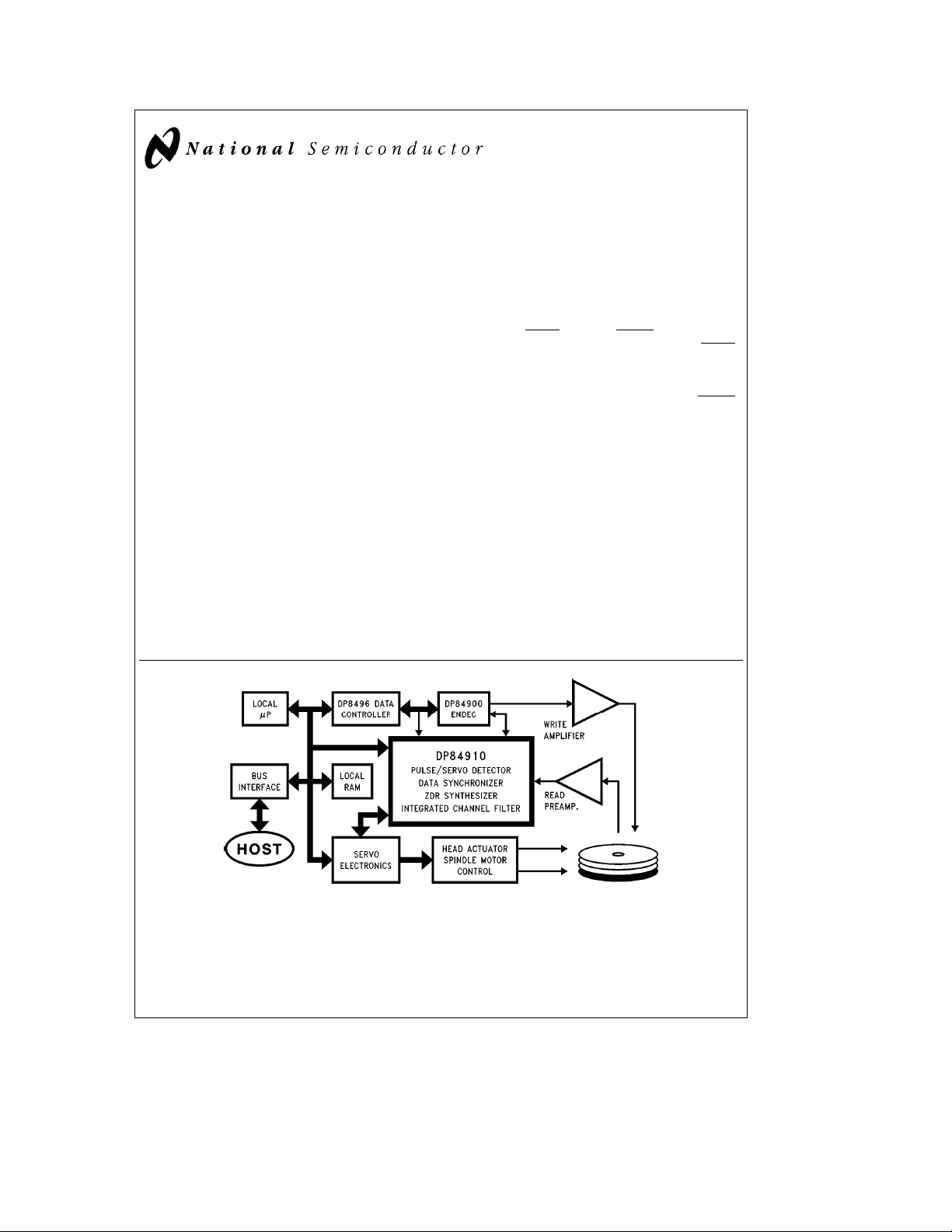
FIGURE 1. DP84910 in a Typical Disk Drive System
MICROWIRETMis a trademark of National Semiconductor Corporation.
C
1996 National Semiconductor Corporation RRD-B30M116/Printed in U. S. A.
TL/F/11777
TL/F/11777– 1
http://www.national.com
Page 2

General Description (Continued)
The pulse detector section detects the peaks of the analog
pulses from the read preamplifier and converts them to digital pulses whose leading edges represent the time position
of the analog pulses’ peaks. In order to not interpret noise
on the baseline as input data, hysteresis is included. The
hysteresis level for a data field is set at the SETHYSD pin
while the hysteresis level for a servo field is set at the
SETHYSS pin. A third pin (SFIELD) is used to select between these two levels of hysteresis. This allows for the
setting of different hysteresis levels for these two fields. The
data field hysteresis level is also selectable in 8 steps
through bits in the control register (HYSÐVTH0–HYS
VTH2) with the level set at the SETHYSD pin as the nominal
value.
The pulse detector section includes an automatic gain control (AGC) circuit which normalizes the analog data signal to
a constant amplitude. The response of the AGC is partially
controlled by one of the device’s pins (VAGCIN). Two
VAGCIN pins (VAGCIND, VAGCINS) are provided so that
different capacitor values can be selected to provide different AGC time constants for data and servo field information.
The switching between these pins/capacitors is controlled
by the SFIELD pin. The SERVO
able (or disable) the SFIELD pin’s ability to control the
amount of equalization provided to the on-chip channel filter. When enabled, the state of the SFIELD pin selects between two groups of control register bits (EQ0, EQ1, EQ2
and SERVOÐEQ0, SERVOÐEQ1, SERVOÐEQ2) which
can separately determine the amount of equalization provided. This feature allows for an adjustment of the channel
filter bandwidth in a servo field. Thus the channel filter can
have different bandwidths in a servo field and a data field.
The pulse detector section has a delayed, low impedance
switch at the gain controlled amplifier inputs (AMPIN1, AMPIN2) which allows for rapid recovery from the write mode.
The amount of delay (either 1.7 msor3.4ms) coming out of
the low impedance mode is selectable through a bit in the
control register (SLOW
). A pattern insensitive, fast responding AGC circuit (with HOLD function) allows rapid head
switch settling and embedded servo normalization. Selectable delay (in four steps) in the qualification channel, along
with a ‘‘view internal signals’’ mode, allow the timing and
qualification channels to be optimally aligned. Four gated
servo detectors are incorporated for recovery of quadrature
embedded servo information. The four peak detected values are available at the SERVO CAPACITOR outputs
(SCAP1–4). Two servo difference amplifiers are provided.
Each difference amplifier output (DIFFAMP1/2) provides
the difference between two of the servo peak detectors,
centered about an external reference voltage (VDIFF).
The channel filter section is a seven-pole 0.05 degree error,
equal ripple filter. It utilizes the Kost pulse slimming technique similar to that which is employed on the DP8491/92
integrated read channel devices. The amount of pulse slimming is control register selectable in 8 steps up to a maximum of 9 dB measured from the base frequency. The bandwidth of the filter is derived from the XTLIN frequency; from
this point, the
b
3 dB frequency is selectable via 7 bits in the
control register (FILTÐ3dBÐ0–FILTÐ3dBÐ6).
control register bit can en-
The data synchronizer section incorporates zero-phasestart (ZPS) and digitally controlled window strobe functions.
The voltage controlled oscillator (VCO) is fully integrated,
requiring no external components, and provides a wide dynamic range necessary for zoned data rate applications.
Data windowing is based on precise VCO duty cycle symmetry (in contrast to delay line based centering). An internal
silicon delay line, used to establish the phase detector retrace angle, automatically tracks zoned data recording data
rate changes. The charge pump output (CPO) and voltage
controlled oscillator input (VCOI) are provided as separate
Ð
pins, allowing ample design flexibility in the external loop
filter. Frequency lock may be employed within the synchronization field. Charge pump (phase detector) gain may be
selected to remain constant or to vary either by a factor of
two or four as instructed via the charge pump gain pin
(CPGAIN) and a bit in the control register (CPRATIO).
The frequency synthesizer section, capable of producing a
large number of frequencies from a single external reference source, generates the write clock and reference frequency for the synchronizer. This section includes a phase
locked loop (PLL) with selectable dividers at the input port
and in its feedback loop. The values for the dividers are
controlled by two control words within the control register.
The user has full control over both the input (five bit word,
PDATA6–PDATA10) and feedback (six bit word, PDATA0 –
PDATA5) divider selection. The feedback divider has an extra bit when compared to previous NSC integrated read
channel circuits to improve the resolution of frequency setting. All blocks within the synthesizer, except the RC loop
filter, are fully integrated. The loop filter resides external to
the chip giving the user full control over the phase locked
loop’s dynamics.
This device is available in an 80-pin 12 mm x 12 mm PQFP
package and operates off of a single
a
5V supply.
Features
Y
Operates at NRZ data rates up to 50 Mbits/sec (equivalent 2/3 (1,7) code data rate)
Y
Operates with a singlea5V power supply
Y
Multiple power down modes available with dedicated
SLEEP
Y
Y
Y
Y
Y
Y
Y
Y
and IDLE/SERVO power down pins
Sleep mode included where I
Directly addresses zoned data recording requirements
e
2 mA maximum
CC
Ð Integrated channel filter with selectable equalization
and bandwidth eliminates multiple external filter elements
Ð Fully integrated frequency synthesizer on-chip to pro-
vide write clock and center frequency for the synchronizer
Selectable delay impedance switch (clamp) at pulse detector input for rapid recovery from the write mode
Pattern insensitive fast AGC for rapid head switch settling and embedded servo normalization
Built-in AGC hold for embedded servo
Two AGC control voltage pins providedÐone for servo
field and one for data field
Four gated detectors for quadrature embedded servo
information
Two servo difference amplifiers on-chip
http://www.national.com 2
Page 3
Features (Continued)
Y
Reference voltage input pin provided for the servo difference amplifiers
Y
Two selectable hysteresis control pins providedÐone
for servo field and one for data field
Y
Data field hysteresis level is control register selectable
in eight steps
Y
Logic polarity for write gate assertion is control register
selectable
Y
Capability provided for different channel filter bandwidths for servo and data fieldsÐchange on the fly with
no settling issues
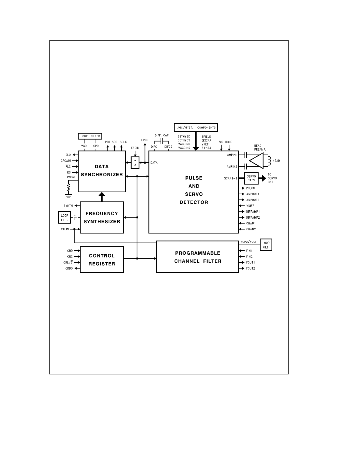
General Block Diagram
Y
Selectable qualification channel delay
Y
Dual gain synchronizer requiring no external or internal
center frequency setting components, external adjustments, or precision components
Y
Digitally controlled synchronizer window strobing
Y
Zero-phase-start synchronizer lock acquisition
Y
Two port synchronizer PLL filtering
Y
Frequency lock option for 2T or 3T synchronization
field (preamble)
Y
TTL compatible inputs and outputs
Y
Chip configurable through serial port interface
FIGURE 2
TL/F/11777– 2
http://www.national.com3
Page 4
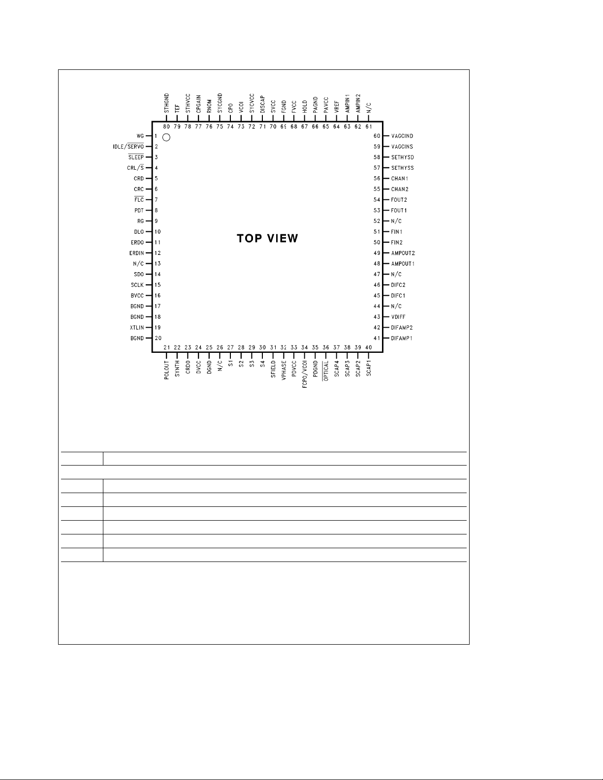
Connection Diagram
Note: Make no external connections to the NSC test pins. TL/F/11777– 3
Order Number DP84910VHG-36 or DP84910VHG-50
See NS Package Number VHG80A
FIGURE 3
Pin Definitions
Ý
Pin
POWER SUPPLY AND GROUND PINS
16 INPUT/OUPUT BUFFER SUPPLY VOLTAGE (BVCC): 5Va5/b10%
17, 18, 20 INPUT/OUTPUT BUFFER GROUNDS (BGND)
24 PLL DIGITAL SUPPLY VOLTAGE (DVCC): 5Va5/b10%
25 PLL DIGITAL GROUND (DGND)
33 PULSE DETECTOR DIGITAL SUPPLY VOLTAGE (PDVCC): 5Va5/b10%
35 PULSE DETECTOR DIGITAL GROUND (PDGND)
http://www.national.com 4
Description
Page 5
Pin Definitions (Continued)
Ý
Pin
POWER SUPPLY AND GROUND PINS (Continued)
65 PULSE DETECTOR ANALOG SUPPLY VOLTAGE (PAVCC): 5Va5/b10%
66 PULSE DETECTOR ANALOG GROUND (PAGND)
68 FILTER ANALOG SUPPLY VOLTAGE (FVCC): 5Va5/b10%
69 FILTER ANALOG GROUND (FGND)
72 SYNCHRONIZER PLL ANALOG SUPPLY VOLTAGE (SYCVCC): 5Va5/b10%
75 SYNCHRONIZER PLL ANALOG GROUND (SYCGND)
78 SYNTHESIZER PLL ANALOG SUPPLY VOLTAGE (STHVCC): 5Va5/b10%
80 SYNTHESIZER PLL ANALOG GROUND (STHGND)
TTL LEVEL LOGIC PINS
1 WRITE GATE INPUT (WG): This pin receives the write mode control input signal from the controller. The logic polarity
for WG assertion is selectable via a bit in the control register (INVÐWG, Bank (1,1) bit 5). WG is active low if the control
register bit is set to invert (INVÐWG
held in a low impedance state and the automatic gain control of the puIse detector is in the hold mode. There are no
setup or hold timing restrictions on WG enabling or disabling.
2 IDLE/SERVO BAR POWER DOWN INPUT (IDLE/SERVO): This input controls the power status of the servo detection
circuitry in the pulse detector. When high (idle mode), this pin powers down all pulse detector circuitry except for biasing
circuitry necessary for quick recovery (k15 ms) from this mode. When low (servo mode), this pin powers on the circuitry
necessary for servo information detection in the puIse detector. The synchronizer and synthesizer power are unaffected
by this pin. The controI register power is also unaffected by the IDLE/SERVO
register’s input’s are only powered on when the IDLE/SERVO
when the IDLE/SERVO
pin.
3 SLEEP BAR POWER DOWN INPUT (SLEEP): This active low input powers down aIl circuitry on the chip. The control
register is powered down in this mode thus it does not retain its information. The control register wiII be reset to the
initial power-on conditions when exiting the sleep mode. The maximum supply current in the sleep mode is 2 mA.
4 CONTROL REGISTER LATCH/SHIFT BAR INPUT (CRL/S): A logical low on this input allows the CONTROL
REGISTER CLOCK input to shift data into the control register’s shift register via the CONTROL REGISTER DATA input.
A positive transition latches the data into the addressed bank of latches and issues the information to the appropriate
circuitry within the device. To minimize power consumption, this pin should be kept at a logical high state except when
shifting data into the control register. The SLEEP
IDLE/SERVO
5 CONTROL REGISTER DATA INPUT (CRD): ControI register data input.
6 CONTROL REGISTER CLOCK INPUT (CRC): Positive-edge-active control register clock input.
7 FREQUENCY LOCK CONTROL BAR INPUT (FLC): This input enables or disables the frequency lock function during a
read operation. It has no effect when READ GATE is disabled. Frequency lock is automatically employed for the full
duration of the time READ GATE is disabled regardless of the level of this input. When READ GATE is taken to a logical
high level while FLC
(2T or 3T sync. field) selected in the control register (PREAMÐ2T, Bank (1,1) bit 4). When FLC
level, the frequency lock action is terminated and the PLL employs a pulse gate to accommodate random disk data
patterns. There are no setup or hold timing restrictions on the positive-going transition of FLC
8 PREAMBLE DETECTED OUTPUT (PDT): This output issues a logical high state after the following sequence; the
enabling of READ GATE, the completion of the zero-phase-start sequence and the detection of approximately 16
sequential pulses of 2T or 3T preamble. Following preamble detection, this output remains latched high until READ
GATE is disabled. This output will be at a logical low state whenever READ GATE is inactive (low).
9 READ GATE INPUT (RG): This input receives the read mode control input signal from the controller, active high for a
read operation. There are no setup or hold timing restrictions on RG enabling or disabling.
10 DELAY LINE OUTPUT (DLO): This active low, open collector output pin issues encoded read data (ERD) delayed by
the selected value in the delay line at the input to the synchronizing latch. By viewing this signal’s phase, the user can
directly view the amount of window movement as the control register’s strobe bits are changed.
pin is high. The contents of the controI register is not affected by the state of the IDLE/SERVO
e
low) in order to shift data into the control register.
is at a logical low level (frequency lock enabled), the PLL is forced to lock to the pattern frequency
e
1). When WG is active, the pulse detector inputs (AMPIN1 and AMPIN2) are
Description
pin but its input buffers are. The control
pin is low. Thus, the controI register cannot be loaded
and IDLE/SERVO pins must be disabled (SLEEPehigh and
is taken to a logical high
.
http://www.national.com5
Page 6
Pin Definitions (Continued)
Ý
Pin
TTL LEVEL LOGIC PINS (Continued)
11 ENCODED READ DATA OUTPUT (ERDO): This output issues the raw, pulsed output of the pulse detector when
enabled by the control register bits ERD0 and ERD1 (Bank (1,1), bits 3 and 4). When disabled (see Table III) this output
will be high. When enabled, the pulsed data from the pulse detector can continue to be issued to the synchronizer
depending on the combination of states of the ERD0 and ERD1 control register bits. When both the ERD0 and ERD1
control register bits are high, the part is put into a test mode where the gain of the GCA is held constant (i.e. fixed gain
mode). In this test mode the synchronizer and synthesizer VCOs can be driven by external test signals.
12 ENCODED READ DATA INPUT (ERDIN): This pin is the input to the synchronizer. It is enabled/disabled via control
register bits ERD0 and ERD1 (Bank (1,1), bits 2 and 3). When enabled (see Table III), this buffer admits external pulsed
data to the synchronizer via this pin and raw data output from the pulse detector is NOT internally fed to the
synchronizer. This allows for testing/exercising of the synchronizer, or for external processing of the peak-detected
data prior to being fed to the synchronizer. When ERDO is disabled, the pulse detector’s data is fed internally to the
synchronizer. When both the ERD0 and ERD1 control register bits are high, the part is put into a test mode where the
gain controlled amplifier is put into a fixed gain. In this test mode the synchronizer and synthesizer VCOs can be driven
by external test signals.
14 SYNCHRONIZED DATA OUTPUT (SDO): This output issues resynchronized data directly from the synchronizing PLL
block.
15 MULTIPLEXED SYNCHRONIZED CLOCK OUTPUT (SCLK): This output issues either the synchronizer or synthesizer
clock signal dependent on whether the device is in the read or non-read mode. The synchronizer clock is selected
during read mode while the synthesizer clock is selected during non-read mode. Multiplexing is done without glitches.
19 CRYSTAL INPUT (XTLIN): This input is the synthesizer and filter reference frequency input. It is designed for
connection from a TTL frequency source. Duty cycle is not critical. An input attenuation resistor is normally used to
minimize transient noise at this pin.
21 POLARITY OUTPUT (POLOUT): This TTL output issues a signal that is the output of the pulse detector’s comparator
with hysteresis. The logical polarity of this signal corresponds to the polarity of the signal at the channel input pins.
22 SYNTHESIZER REFERENCE OUTPUT (SYNTH): This output issues a continuous reference signal from the frequency
synthesizer when enabled. At V
a bit in the control register (ENSTHO
rate.
23 CONTROL REGISTER DATA OUTPUT (CRDO): This output issues data from the control register. It can be connected
to the input of another device’s control register such as the DP84900 (ENDEC) so that the number of data lines from
the controller can be minimized.
27–30 SERVO SWITCH INPUTSÝ1,Ý2,Ý3,Ý4 (S1, S2, S3, S4): These pins, in conjunction with the AGC HOLD pin,
control the gating action of the gated servo peak detectors and the discharge of the servo channeIs. These pins also
enabIe or disabIe the output internal signals, the track follow and the seek modes according to Table IV.
31 SERVO FIELD SELECT INPUT (SFIELD): When at a high logic level, this pin switches the hysteresis threshold control
of the puIse detector’s comparator from the SET HYSTERESIS-DATA FIELD (SETHYSD) pin to the SET
HYSTERESIS-SERVO FIELD (SETHYSS) pin. It also switches the AGC controI from the AGC control capacitor-data
field (VAGCIND) pin to the AGC control capacitor-servo field (VAGCINS) pin. When enabled by a control register bit
e
(SERVO
filter, between data equalization control bits (EQ0, EQ1, EQ2, Bank (0,0) bits 9, 10, 11) and servo equalization control
bits (SERVOÐEQ0, SERVOÐEQ1 SERVOÐEQ2, Bank (1,1) bits 10, 11, 12).
36 OPTICAL: The optical (unipolar) mode is enabled by the application of ground to this pin. For magnetic operation this
pin must be left open (no connection to it). Refer to design guide for details of operation.
67 COAST/AGC HOLD INPUT (HOLD): When high, this input controls an internal switch which freezes the pulse detector
AGC level for the reading of the servo burst. Phase comparisons within the synchronizer (read mode only) are also
disabled, allowing the PLL to coast.
77 CHARGE PUMP GAIN INPUT (CPGAIN): This input selects the gain of the synchronizer’s charge pump in conjunction
with a bit in the control register (CPRATIO, Bank (1,0) bit 12) (see Table VIII).
1, Bank (0,0) bit 12), this pin can switch the equalization, and consequently the bandwidth of the channel
power up this pin is in the inactive state (a logical high state) and can be enabled via
CC
, Bank (1,0) bit 5). The output frequency will be the same as the media code clock
Description
http://www.national.com 6
Page 7

Pin Definitions (Continued)
Ý
Pin
ANALOG SIGNAL PINS
32 VPHASE: An internally generated voltage is present at his pin to control the Q of the integrated filter. An external
network (24 kX to FV
34 FILTER CHARGE PUMP OUTPUT/VCO INPUT NODE (FCPO/VCOI): This is the filter node for the channel filter PLL.
An externaI resistor and capacitor loop filter is tied in series between this pin and ground.
37 SERVO CAPACITORÝ4 (SCAP4): This pin is the connection point for the peak detector capacitor for the embedded
servo gated detector. The DC level on this capacitor represents the amplitude of one of four servo bursts. When the
‘‘output internal signals’’ mode is selected by applying a high logical level to the S2 pin and a low logical level on the
HOLD pin, the signal on this pin becomes the output of the seIectable delay block in the qualification channel (see
Table IV).
38 SERVO CAPACITORÝ3 (SCAP3): This pin is the connection point for the peak detector capacitor for the embedded
servo gated detector. The DC level on this capacitor represents the amplitude of one of four servo bursts. When the
‘‘output internal signals’’ mode is selected by applying a high logical level to the S2 pin and a low logical level on the
HOLD pin, the signal on this pin becomes the output of the time channel zero-cross detector (see Table IV).
39 SERVO CAPACITORÝ2 (SCAP2): This pin is the connection point for the peak detector capacitor for the embedded
servo gated detector. The DC level on this capacitor represents the amplitude of one of four servo bursts. When the
‘‘output internal signals’’ mode is selected by applying a high logical level to the S2 pin and a low logical Ievel on the
HOLD pin, the signal on this pin becomes one of the differential outputs of the differentiator (see Table IV).
40 SERVO CAPACITORÝ1 (SCAP1): This pin is the connection point for the peak detector capacitor for the embedded
servo gated detector. The DC level on this capacitor represents the amplitude of one of four servo bursts. When the
‘‘output internal signals’’ mode is selected by applying a high logical level to the S2 pin and a low logical level on the
HOLD pin, the signal on this pin becomes one of the differential outputs of the differentiator (see Table IV).
41, 42 SERVO DIFFERENCE AMPLIFIERS OUTPUTSÝ1,Ý2 (DIFAMP1, DIFAMP2): These low impedance pins issue an
output signal which is the difference in voltage between SCAP4 and SCAP3 pins (DIFAMP2) and SCAP2 and SCAP1
pins (DIFAMP1). These differences will be centered about a reference level set by the voltage on the VDlFF pin.
43 SERVO DIFFERENCE VOLTAGE REFERENCE INPUT (VDIFF): A voltage applied to this pin provides a reference for
the zero-level of the signals issued by the difference amplifiers on DIFAMP1 and DIFAMP2 pins.
45, 46 DIFFERENTIATOR CAPACITOR NODESÝ1,Ý2 (DIFC1, DIFC2): These pins are connection points for the
differentiator components (typically a resistor, capacitor, and inductor).
48, 49 GAIN CONTROLLED AMPLIFIER OUTPUTSÝ1,Ý2 (AMPOUT1, AMPOUT2): These pins are complimentary emitter
follower outputs from the gain controlled amplifier. They are to be externally capacitively coupIed to the channel filter
inputs (FIN1, FIN2).
50, 51 FILTER INPUTSÝ2,Ý1 (FIN2, FIN1): These channel filter inputs are to be externally capacitively coupled to the gain
controlled amplifier outputs (AMPOUT1, AMPOUT2).
53, 54 FILTER OUTPUTSÝ1,Ý2 (FOUT1, FOUT2): These pins are complimentary emitter foIIower outputs from the channeI
filter. They are to be externally capacitively coupled to the timing-gating channel/AGC sense/servo channel inputs
(CHAN1, CHAN2).
55, 56 TIMING-GATING CHANNEL/AGC SENSE/SERVO INPUTSÝ2,Ý1 (CHAN2, CHAN1): These input pins are to be
externally capacitively coupled from the channel filter outputs (FOUT1, FOUT2). These pins are the inputs to the
differentiator, AGC amplifier, servo channel and qualification channel.
57 SET HYSTERESIS INPUT-SERVO FIELD (SETHYSS): When activated by a logical high level on the SFIELD pin, the
voltage applied to this pin determines the amount of hysteresis for the pulse detector’s hysteresis comparator. This
level should be set high enough to eliminate noise which might occur in the shoulder region between read pulses from
the preamplifier. The SVCC pin is provided to be used as a supply reference for a resistive divider to set this level.
58 SET HYSTERESIS INPUT-DATA FIELD (SETHYSD): When activated by a logical low level on the SFlELD pin, the
voltage applied to this pin in conjunction with three control register bits (HYSÐVTH0, HYSÐVTH1, HYSÐVTH2,
Bank (1,1), bits 7, 8, 9) determines the amount of hysteresis for the pulse detector’s hysteresis comparator. This level
should be set high enough to eliminate noise which might occur in the shouIder region between read pulses from the
preamplifier. The SVCC pin is provided to be used as a supply reference for a resistive divider to set this level.
59 SERVO FIELD AUTOMATIC GAIN CONTROL VOLTAGE INPUT (VAGCINS): When activated by a logical high level
on the SFIELD pin, the voltage at this pin controls the gain of the gain controlled amplifier.
and 18 kX to GND) should be connected to this pin to optimize the filter’s performance.
CC
Description
http://www.national.com7
Page 8
Pin Definitions (Continued)
Ý
Pin
ANALOG SIGNAL PINS (Continued)
60 DATA FIELD AUTOMATIC GAIN CONTROL VOLTAGE INPUT (VAGCIND): When activated by a logical low level on
the SFIELD pin, the voltage at this pin controls the gain of the gain controlled amplifier.
62, 63 AMPLIFIER INPUTSÝ2,Ý1 (AMPIN2, AMPIN1): These inputs accept the preamplified, analog, coded data signal
read from the disk. They are to be externally capacitively coupled from the preamplifier. They go to a low impedance
state when WRITE GATE is enabled and remain low impedance for either 1.7 msor3.4ms (selectable by control
register bit, SLOW
remove DC offsets accumulated across the amplifier input coupling capacitors during the write mode.
64 AGC REFERENCE VOLTAGE INPUT (VREF): This input provides the reference voltage to the AGC circuit for
controlling the peak-to-peak signal swing at the channel input pins. The voltage on this pin corresponds directly to the
peak-to-peak channel input signal level. A resistor divider between supply and ground can be used to provide this
voltage. The SVCC pin is provided to be used as a supply reference.
70 SWITCHED SUPPLY VOLTAGE (SVCC): This emitter-follower output may be used as the supply for the external VREF
resistor voltage divider and for both the external servo and data hysteresis resistor voltage dividers. The voltage at this
pin will typically be V
71 DISCHARGE CAPACITOR (DISCAP): A capacitor is tied from this pin to ground to establish an RC time constant which
sets the minimum operational frequency and decay characteristics of the AGC. The voltage at this pin can also be used
for dynamic hysteresis. Note, unlike the DP8491/92 which requires an RC combination tied to this pin, the DISCAP pin
has an internal 10 kX resistor connected to ground. Thus, only an external capacitor is required to set the RC time
constant.
73 VOLTAGE CONTROLLED OSCILLATOR INPUT (VCOI): This pin is the input to the voltage control block for the
synchronizer VCO and is to be connected to the external loop filter output.
74 CHARGE PUMP OUTPUT (CPO): This pin issues the signal from the synchronizer PLL charge pump and is to be
connected to the external loop filter input.
76 RNOMINAL (RNOM): A resistor connected from this pin to ground sets the synchronizer charge pump current.
79 TIMING EXTRACTOR FILTER (TEF): This pin is the filter node for the synthesizer phase locked loop (PLL). An
external resistor and capacitor loop filter is tied in series between this pin and ground.
, Bank (1,1) bit 6, 0e3.4 ms) after WRITE GATE is disabled. This low impedance state is used to
b
1V. The voltage at this pin goes low in the sleep mode.
CC
Description
http://www.national.com 8
Page 9
Power Down Operation
The DP84910 has several methods available to control or
manage device power consumption. Three control register
bits and two pins are provided to control the power status of
elements in this device. The control register bits control the
power status of the pulse detector (PDÐPWRÐDN, Bank
(1,0) bit 4), synchronizer (SYNCÐPWRÐDN, Bank (1,0) bit
2) and synthesizer (STHÐPWRÐDN, Bank (1,0) bit 3). The
device is configured to initially power up with the synchronizer, synthesizer and pulse detector powered down. The control register power is controlled only by the SLEEP
The SLEEP
pin is one of the two pins available for power
management. This pin powers down all circuitry on the chip
including the control register. In this mode the maximum
power supply current is 2 mA. The control register latches
are preset into specific states when exiting the sleep mode.
The shift register flip-flops, however, are in indeterminate
states until all 13 bits have been shifted in. Note that if the
CRL/S
input is given a positive transition after exiting the
sleep mode but before valid data has been entered into
the shift register, the indeterminate contents of the shift reg-
TABLE I. Selective Power Down Truth Table
Pin
IDLE/
SERVO
Pin
SLEEP
0 X X X X OFF OFF OFF OFF
1 1 0 0 0 OFF* ON** ON ON
1 1 0 0 1 OFF* ON** OFF ON
1 1 0 1 0 OFF* ON** ON OFF
1 1 0 1 1 OFF* ON** OFF OFF
10000ONONONON
1 0 0 0 1 ON ON OFF ON
1 0 0 1 0 ON ON ON OFF
1 0 0 1 1 ON ON OFF OFF
1 X 1 0 0 OFF ON** ON ON
1 X 1 0 1 OFF ON** OFF ON
1 X 1 1 0 OFF ON** ON OFF
1 X 1 1 1 OFF ON** OFF OFF
*Except for pulse detector circuitry biasing necessary for quick recovery from power down mode.
**Control register buffers powered down. Data in register will not be affected but new data cannot
be loaded into register when IDLE/SERVO
pin.
Ctrl Reg.
Bank (1,0)
B4 B3 B2
ister will be randomly loaded into one of the four banks of
latches. Although the sleep mode can be safely exited with
the CRL/S
into the shift register before CRL/S
pin either high or low, valid data must be loaded
is given a positive tran-
sition.
The IDLE/SERVO
pin is the second of the two pins available for power management. This pin toggles the device
between the idle and servo modes. In the idle mode, only
the control register and pulse detector biasing circuitry necessary for a quick recovery from the power down mode are
active. In the servo mode, the pulse detector portions needed for servo detection are active as well as the control register. Less than 15 ms is required for the pulse detector to
recover from the idle condition. The control register data is
not lost when this pin is toggled. This pin does not control
the power status of the synchronizer or synthesizer. To
achieve maximum power savings during extended servoonly activity, the synchronizer and synthesizer should be
powered down.
Power Status by Block
PD &
SERVO
is high.
CR SYNCH SYNTH
http://www.national.com9
Page 10
Absolute Maximum Ratings are those
values beyond which the safety of the device cannot be
guaranteed. The device should not be operated at these
limits. The parametric values defined in the ‘‘Electrical Characterisitics’’ tables are not guaranteed at these ratings. The
‘‘Operating Conditions’’ table will define the conditions for
actual device operation.
Supply Voltage 7V
TTL Input Maximum Voltage 7V
Maximum Output Voltage 7V
Maximum Input Current (Analog Pins) 2 mA
(or as specified on per-pin basis)
ESD Susceptibility 1500V
(Note 1)
Operating Conditions guaranteed over operating temperature and supply voltage ranges unless otherwise speci-
fied. Minimum and/or maximum limits are guaranteed by outgoing testing unless otherwise specified.
Symbol Parameter Conditions Min
V
T
T
I
OH
I
OL
V
V
C
f
NRZ
CC
A
S
IH
IL
L
Supply Voltage 4.5 5.0 5.5 V
Operation Ambient Temperature 0 70
Storage Temperature
High Logic Level Output Current for TTL Outputs (Note 2)
Low Logic Level Output Current for TTL Outputs (Note 2) 8 mA
High Logic Level Input Voltage 2 V
Low Logic Level Input Voltage 0.8 V
Capacitive Load on Any TTL Output (Note 2) 15 pF
NRZ Transfer Rate Operating Frequency -36 7.5 36
-50 13.7 50
f
VCO
f
STH
f
XTL
t
PWH(XTL)
t
PWL(XTL)
t
PWH(ERDIN)
t
PWL(ERDIN)
t
PW(CRL/S)
t
SU(CRD)
t
H(CRD)
t
SU(CRL/S)
t
H(CRL/S)
t
PW(CRC)
I
RNOM
Note 1: Human body model is used. (120 pF through 1.5 kX)
Note 2: Parameter guaranteed by design or correlation data. No outgoing tests are performed.
Note 3: Typical values are specified at 25
Synchronizer VCO Operating Frequency (Note 2) 1.5 f
Synthesizer VCO Operating Frequency (Note 2) 1.5 f
Crystal Input Operating Frequency (Note 2) 20 MHz
Width of XTLIN Pulse (High) 20 ns
Width of XTLIN Pulse (Low) 20 ns
Width of ERDIN Pulse (High) 15 9 ns
Width of ERDIN Pulse (Low) 10 5 ns
Width of CRL/S Pulse (High or Low) (Note 2) 50 ns
CRD Setup Time with Respect to CRC (Note 2) 20 ns
CRD Hold Time with Respect to CRC (Note 2) 20 ns
CRL/S Setup Time with Respect to CRC (Note 2) 200 ns
CRL/S Hold Time with Respect to CRC (Note 2) 20 ns
CRC Pulse Width (High or Low) (Note 2) 25 ns
RNOM Pin Current 90 130 170 mA
C and 5V supply.
§
b
Typ
(Note 3)
Max Units
65 150
b
400 mA
NRZ
NRZ
C
§
C
§
Mb/s
MHz
MHz
http://www.national.com 10
Page 11

DC Electrical CharacteristicsÐGeneral guaranteed over operating conditions (see table) unless oth-
erwise specified. Minimum and/or maximum limits are guaranteed by outgoing testing unless otherwise specified.
Symbol Parameter Conditions Min
e
e
e
e
e
e
V
Min, I
Min, I
Min, I
Max, V
Max, V
Max, V
CPO
I
OH
OL
k
eb
e
e
e
I
e
I
e
O
2.5V
18 mA
Max
Max
2.7V
0.4V
2.125V (Note 1)
V
0.8 K
V
IC
V
OH
V
OL
I
IH
I
IL
I
O
I
CPO
I
DRIFT
Input Clamp Voltage V
High Logic Level V
Output Voltage
Low Logic Level V
Output Voltage
High Logic Level V
Input Current
Low Logic Level V
Input Current
Output Drive Current V
CC
CC
CC
CC
CC
CC
Charge Pump Output (Note 2)
Current
Combined Charge Charge Pump Inactive, CPO and VCOI
Pump Output
Inactive Current and 1V
pins tied together
k
VCOI OFFSET
Current
I
TEF
I
TEF-OFF
V
RNOM
V
CPO(PD)
TEF Output Current 1VkV
(Absolute Value)
TEF Output Inactive 1VkV
Current
Voltage at RNOM Pin I
CPO Voltage with
RNOM
b
Synchronizer
TEF
TEF
e
5 mAkI
k
2.5V
k
2.5V
125 mA, 25
k
5 mA
CPO
C only 0.6 0.75 0.9 V
§
Powered Down
V
TEF(PD)
TEF Voltage with
Synthesizer Powered
b
5 mAkI
TEF
k
5 mA
Down
I
CCR
Supply Current in the V(WG)e0.3V, All Sections 16.7 Mb/s 160 190 mA
Read Mode Powered On. V
CC
e
5.25V
33.3 Mb/s 175 200 mA
50 Mb/s 200 220 mA
I
CC(SLEEP)
I
CC(IDLE)
I
CC(PD)
Supply Current in V(SLEEP)e0.8V, V
Sleep Mode
Supply Current in Idle V(WG)e0.3V Power Down
Mode
Synchronizer and Synthesizer Sections
of the Chip Via Control Register. Power
Down Pulse Detector with IDLE Pin.
e
V
5.25V
CC
Pulse Detector V(WG)e0.3V. Power Down All Sections
Supply Current with
All Other Sections
of the Chip Via Control Register Except
the Pulse Detector. V
CC
CC
e
e
5.25V
5.25V
Powered Down
V
SVCC
Note 1: V
Note 2: K1 is the selected charge pump gain constant (2, 4 or 8), I
Note 3: Typical values are specified at 25
Switched Supply SLEEPeHIGH. Pull 1 mA from SVCC
) Output
(SV
CC
Voltage
e
2.125V produces a current closely approximating one half of the true short circuit current, IOS.
O
pin.
C and 5V supply.
§
e
I
RNOM
,1VkV
IN
CPO
k
2.5V.
V
CC
b
0.65 1
b
CC
b
12
1IIN
b
1.2 1.2 mA
250 800 mA
b
11mA
1.1 1.5 2 V
1.1 1.5 2 V
b
Typ
(Note 3)
2V
b
1.6 V
CC
0.25 0.5 V
120mA
b
60
K1I
IN
1 2.5 mA
10 20 mA
CC
b
1V
1.1 V
Max Units
b
1.5 V
b
200 mA
b
110 mA
1.2 K1I
IN
110 mA
b
0.9 V
CC
http://www.national.com11
Page 12

DC Electrical CharacteristicsÐPulse Detector, Servo and Filter guaranteed over
operating conditions (see table) unless otherwise specified. Minimum and/or maximum limits are guaranteed by outgoing testing
unless otherwise specified.
Symbol
Z
IN-AL
AV
A(MAX)
AV
A(MIN)
AV
A(FG)
V
Aob
V
TH(AGC)
Gm
AGC
b
I
AGC(SLEW)
I
AGC(SLEW)
FSBP AGC Fast Slew Break Point for V
V
DISCAP
I
LEAK(AGC)H
I
LEAK(AGC)W
I
LEAK(AGC)ID
Z
DISCAP
Z
IN(AL)W
I
clamp(sink)
I
clamp(source)
Z
IN(CH)
Circuit
Block (Note 24)
Parameter Conditions Min
GCA Amplifier Input Impedance Nonwrite Mode (Note 1)
(AMPIN1, AMPIN2)
GCA Maximum Amplifier Gain V
GCA Minimum Amplifier Gain V
VAGCIN
VAGCIN
e
1V (Note 2) 50 V/V
e
4V (Note 2) 0.1 0.5 V/V
GCA Amplifier Gain in Fixed Control Register Programmed
Gain Mode for Fixed Gain Mode (Note 2)
GCA Amplifier Output DC Bias
Level
AGC AGC Threshold Voltage V
AGC AGC Transconductance V
AGC AGC Slew Current
(Flowing out of either V
VAGCINS or VAGCIND)
AGC AGC Slew Current
(Flowing into either V
VAGCINS or VAGCIND)
AGC V
REF
V
VAGCIN
VAGCIN
V
l
CHAN1
VAGCIN
V
l
CHAN1
VAGCIN
VACGIN
REF
e
0.5V,
e
2.5V (Note 3)
e
2.5V (Note 4) 0.7 1 1.3 mA/V
b
V
CHAN2
e
2.5V, V
b
V
CHAN2
e
2.5V, V
e
2.5V (Note 5)
e
0.5V
AGC Discharge Capacitor Measurement Made at
Voltage V
AGC (Note 23)
TH
AGC AGC Leakage Current in HOLDeHigh, V
AGC Hold Mode 2.5V (Note 6)
AGC AGC Leakage Current Pulse Detector Placed in Write
Write Mode Mode. V
(Note 6)
VAGCIN
AGC AGC Leakage Current in Pulse Detector is in Idle Mode.
Idle Mode V
VAGCIN
e
2.5V (Note 6)
AGC DISCAP Pin Impedence Force 2V on the DISCAP Pin
and Measure the Impedence
AMP. Amplifier Input Impedance (Note 1)
CLAMP in Write Mode
AMP. Amplifier Input Clamp (Note 7)
CLAMP Sink Current
AMP. Amplifier Input Clamp (Note 8)
CLAMP Source Current
CHAN. Channel Input Impedance (Note 1)
INPUTS
H/R(D) CHAN. Ratio of the Data Field See Conditions for
INPUTS Hysteresis Threshold to V
the AGC Threshold (Note 10)
HYSD(101) and VTH(AGC)
TH
H/R(S) CHAN. Ratio of the Servo Field See Conditions for
INPUTS Hysteresis Threshold to VTH(HYSTS) and VTH(AGC)
the AGC Threshold (Note 10)
l
REF
l
REF
VAGCIN
e
2.5V
2 2.4 2.8 kX
8 11 13 V/V
3 3.4 4.4 V
425 500 575 mV
e
0.5V,
e
0.5Vb400
e
0V,
e
0.5V 200 240 400 mA
20 30 40 %
1.3 1.8 2.4 V
e
71115kX
911 mA
912 mA
4.4 4.7 5 kX
0.25 0.37 0.45
0.25 0.36 0.45
Typ
b
240
Max Units
b
180 mA
0.02 0.09 mA
0.02 0.03 mA
0.02 0.07 mA
65 100 X
PP
http://www.national.com 12
Page 13

DC Electrical CharacteristicsÐPulse Detector, Servo and Filter guaranteed over
operating conditions (see table) unless otherwise specified. Minimum and/or maximum limits are guaranteed by outgoing testing
unless otherwise specified. (Continued)
Symbol
I
SETHYS
I
VREF
I
DIFC
V
th(HYSTS)
V
thHYSD(111)
V
thHYSD(110)
V
thHYSD(101)
V
thHYSD(011)
V
thHYSD(000)
Z
SCAP(DIS)
Av
QT(gd)
V
INTERCEPT
GL
gd
V
OSgd
I
Lgd
V
OS(DA)
AV
DA
Circuit
Block (Note 24)
CHAN. Set Hysteresis Input Bias V
INPUTS Current (Note 11)
CHAN. VREF Input Bias Current V
INPUTS
CHAN. Differentiator Bias Current V
INPUTS V
Parameter Conditions Min
SETHYSD
e
REF
e
DIFC2
e
DIFC1
e
0.5V
3.5V or
3.5V
V
SETHYSS
e
0.45V
b
b
1.3 1.8 mA
CHAN. Hysteresis Comparator (Note 9)
INPUTS Threshold Voltage for Servo
194 239
Hysteresis Level
CHAN. Data Field Hysteresis Ctrl Reg. Bits: HYSÐVTHOe1,
INPUTS Comparator Threshold HYSÐVTH1
e
HYSÐVTH2e1 133 159 mV
Voltage (Note 9)
CHAN. Data Field Hysteresis Ctrl Reg. Bits: HYSÐVTH0e0,
INPUTS Comparator Threshold HYSÐVTH2
e
HYSÐVTH1e1 166 201 mV
Voltage (Note 9)
CHAN. Data Field Hysteresis Ctrl Reg. Bits: HYSTÐVTH1e0,
INPUTS Comparator Threshold HYSÐVTH0
e
HYSÐVTH2e1 207 246 mV
Voltage (Note 9)
CHAN. Data Field Hysteresis Ctrl Reg. Bits: HYSÐVTH2e0,
INPUTS Comparator Threshold HYSÐVTH0
e
HYSÐVTH1e1 282 315 mV
Voltage (Note 9)
CHAN. Data Field Hysteresis Ctrl Reg. Bits: HYSÐVTH0
e
INPUTS Comparator Threshold HYSÐVTH1eHYÐVTH2e0 372 418 mV
Voltage (Note 9)
SERVO SCAP Pin Discharge V
Impedance V
SERVO Servo Channel Gain for V
Quarter Track Mispositioning (Note 14)
SERVO Servo Channel Output V
Voltage for 0 V
Input (Notes 13 and 15)
PP
SERVO Gated Detector Gain V
Linearity (Notes 13, 16 and 17)
SERVO Gated Detector Output V
Voltage Offset (Note 18)
SERVO Gated Detector Leakage V
Current V
e
HOLD
SCAP1– 4
e
HOLD
e
HOLD
e
HOLD
e
HOLD
e
V
S1
e
HOLD
0.3V, V
e
3V
4V
4V
4V
S2
4V (Note 19)
S4
2V (Note 12)
e
e
V
S3
e
4V,
4.6 5.5 7.8 V/V
e
V
0.3V,
S4
SERVO Servo Difference (Note 20)
Amplifier Offset Voltage
SERVO Servo Difference Gain is Measured from
Amplifier Gain SCAP Pins to Difference 0.45 0.475 0.5 V/V
Amplifier Output
Typ
b
38
b
30
Max Units
24 mA
15.5 mA
4 6.2 8.5 kX
1 1.4 %
0.3 1 %
10 25 mV
0.02 0.05 mA
512mV
mV
PP
PP
PP
PP
PP
PP
http://www.national.com13
Page 14

DC Electrical CharacteristicsÐPulse Detector, Servo and Filter guaranteed over
operating conditions (see table) unless otherwise specified. Minimum and/or maximum limits are guaranteed by outgoing testing
unless otherwise specified. (Continued)
Symbol
V
DA(MAX)
Circuit
Block (Note 24)
SERVO Maximum Output V
Parameter Conditions Min
e
4.5V (Note
Voltage of Servo 21)
CC
3.2 3.37 V
Difference Amplifier
V
DA(MIN)
SERVO Minimum Output Force SCAP’s to
Voltage of Servo Achieve Minimum
Difference Conditions Output from
Difference
Amplifier
Z
VDIFF
I
DA
I
GDSEEK
SERVO VDIFF Input Impedance V
SERVO Difference Amplifier
Output Drive Capability
SERVO Gated Detector Seek V
Mode Pull Down (Note 22)
e
2.5V 15 33 kX
DIFF
100 170 mA
e
4V
HOLD
5 8.5 12 mA
Current
Av
DF(MAX)
Av
SF(MAX)
Av
DF(MIN)
Av
SF(MIN)
Z
IN(F)
V
FOB
K
CPF
FILTER Maximum Filter Gain in Set Pulse Slimming
Data Field to Min. Peaking.
SFIELD
SERV
e
e
0 (CR bit)
LOW,
0.85 1.33 1.55 V/V
FILTER Maximum Filter Gain in Set Pulse Slimming
Servo Field to Min. Peaking.
SFIELD
SERV
e
e
0 (CR bit)
HIGH,
1.1 1.77 1.95 V/V
FILTER Minimum Filter Gain in Set Pulse Slimming
Data Field to Max. Peaking.
SFIELD
SERV
e
e
0 (CR bit)
LOW,
0.4 0.6 1 V/V
FILTER Minimum Filter Gain in Set Pulse Slimming
Servo Field to Max. Peaking.
SFIELD
SERV
e
e
0 (CR bit)
HIGH,
0.7 1 1.3 V/V
FILTER Filter Input Impedence (Note 1) 3.1 3.8 4.8 kX
FILTER Filter Output DC Bias V
Level Voltage for Minimum Spec.
e
Min.
CC
e
Max.
V
CC
for Maximum Spec.
0.65 0.9 1.4 V
FILTER Charge Pump Current
(Negative) 320 420 500 mA
Channel Filter PLL
K
VCOF
Note 1: The input pin consists of two resistors tied to a voltage source. This is the resistance of each resistor.
Note 2: Gain is measured differentially.
Note 3: The AGC threshold voltage is defined as the equivalent differential peak to peak AC voltage swing across the channel input pins that causes the current at
VAGCIN pin to equal zero.
Note 4: Channel inputs (CHAN1 and CHAN2) are set at V
current at the VAGCIN pin. The measurement is made at V
Note 5: The Fast Slew Break Point (FSBP) is defined as a positive or negative percentage of the AGC threshold voltage (V
above and below V
above and below the AGC threshold, while monitoring the transconductance at the VAGCIN pin. The break point occurs when the transconductance increases by
at least 20% above Gm
Note 6: Measure current into or out of VAGCIN pin for both V
and VAGCIND pins. V
Note 7: The common mode voltage at AMPIN1 and AMPIN2 pins is measured for no current into these pins. Current is then forced into either AMPIN1 or AMPIN2
(not both simultaneously) until the voltage on the pin rises by 1V.
Note 8: The common mode voltage at AMPIN1 and AMPIN2 is measured for no current out of these pins. Current is then pulled out of either AMPIN1 or AMPIN2
(not both simultaneously) until the voltage fails by 1V.
FILTER VCO Gain,
Channel Filter PLL
where the Gm
TH(AGC)
AGC
REF
.
e
0.5V.
AGC
1.4f
XTLIN
a
10 mV. Transconductance is measured from the channel inputs (CHAN1 and CHAN2) to the
TH(AGC)
TH(AGC)
abruptly increases. This point is found by increasing or decreasing the differential voltage at the channel inputs
CHAN1
.Gm
b
AGC
V
CHAN2
e
I
/10 mV
l
VAGCIN
e
0 and V
CHAN1
l
b
e
V
CHAN2
Typ
Max Units
1.05 1.4 V
1.8f
XTLIN
TH(AGC)
0.5V. This specification applies to both VAGCINS
2.3f
XTLIN
). The break point is that voltage
1/V
http://www.national.com 14
Page 15

DC Electrical CharacteristicsÐPulse Detector, Servo and Filter (Continued)
Note 9: The hysteresis comparator threshold is defined as the minimum differential AC signal across the channel inputs (CHAN1 and CHAN2) which causes the
voltage on the POLOUT pin to change state. V
Note 10: The effect that a % change in the H/R ratio has on the qualification threshold, can be calculated by multiplying the H/R % change by the percentage
qualification threshold. For example if the qualification threshold is 30% of the channel input signal and the % change in the H/R ratio is 10%, the net effect on the
qualification level is 30%
Note 11: This specification applies to both SETHYSD and SETHYSS pins.
Note 12: SCAP1, SCAP2, SCAP3 and SCAP4 pins are measured.
Note 13: S1, S2, S3 and S4 pins are at an appropriate level to gate on the channel under test.
V
QTHeThe servo output voltage from the SCAP pins with the channel input level set to simulate the read head mispositioned by one quarter of a track in a
O
direction towards the servo burst (i.e. larger amplitude). This is done by setting Vc1
the voltage on the SCAP pins.
V
QTLeThe servo output voltage from the SCAP pins with the channel input level set to simulate the read head mispositioned by one quarter of a track in a
O
direction away from the servo burst (i.e. smaller amplitude). This is done by setting Vc1
measuring the voltage on the SCAP pins.
Note 14: Av
(QT(gd))
Note 15: Expressed as a percentage of V
Note 16: S1, S2, S3 and S4 pins are at an appropriate level to gate on the channel under test
V
ETHeThe servo output voltage from the SCAP pins with the channel input level set to simulate the read head mispositioned by one quarter of a track in a
O
direction towards the servo burst (i.e. larger amplitude). This is done by setting Vc1
the voltage on the SCAP pins.
V
ETLeThe servo output voltage from the SCAP pins with the channel input level set to simulate the read head mispositioned by one quarter of a track in a
O
direction away from the servo burst (i.e. smaller amplitude). This is done by setting Vc1
measuring the voltage on the SCAP pins.
Note 17: GL
Note 18: Set the voltage at S1, S2 and S3 pins to gate on the channel under test. Force
each gated detector output (SCAP pins). V
Note 19: V
Note 20: Force all SCAP pins to 3V and measure difference between VDIFF and DIFAMP1 and VDIFF and DIFAMP2 pins.
Note 21: Force SCAP pins to achieve maximum output from the difference amplifier.
Note 22: Program seek mode. Force 3V on SCAP pin under test. Gate on servo channel under test. Measure current into SCAP pin.
Note 23: This parameter is V
specified V
Note 24: Typical values are specified at 25
(gd)
CHAN1
CC
c
10%e3%.
e
(VOQTHbVOQTL)/(QTHbQTL).
e
À
[
[
100
VOEHbVOETLl/lVOQTHbVOQTL
l
b
e
V
0V. Force 3V on each of the gated detector output pins (SCAP pins) and measure the current into or out of the pin.
CHAN2
dependent. The minimum specification is at the minimum specified VCC, while the maximum specification is at the maximum
.
CC
.
CC
OSgd
C and 5V supply.
§
e
SETHYSD
e
g
the maximum difference voltage between (SCAP1 –SCAP2) and (SCAP3 –SCAP4)l.
l
V
SETHYSS
]
l
b
0.5Ó/0.5
e
0.45V.
e
b
V
CHAN1
V
CHAN1
V
e
V
375 mVPPdifferentialeQTH and measuring
l
CHAN2
b
V
CHAN2
e
312.5 mVPPdifferentialeETH and measuring
l
CHAN2
b
V
l
CHAN2
e
250 mVPPdifferential. Measure the voltage at
l
CHAN2
V
l
CHAN1
e
l
e
]
V
l
V
l
CHAN1
CHAN1
b
e
V
l
b
e
125 mVPPdifferentialeQTL and
l
e
187.5 mVPPdifferentialeETL and
AC Electrical CharacteristicsÐFilter guaranteed at 25
limits are guaranteed by outgoing testing unless otherwise specified.
Symbol Parameter Conditions (Note 7) Min
DLY
data
BOOST
D(mx)
BOOST
S(mx)
BWAC
D(MXB)
BWAC
D(MNB)
BWAC
S(MXB)
BWAC
S(MNB)
Note 1: With control register bits EQ0, EQ1, EQ2 set to 1 (i.e. no boost), the change in delay is measured from theb3 dB frequency of the filter to one fourth of the
b
3 dB frequency. The change in delay is measured from the inputs of the filter to the output of the filter. This parameter is measured with theb3 dB frequency set
to 10 MHz. This parameter is also guaranteed for control register bits EQ0, EQ1 and EQ2 set to 0 (i.e. full boost), over the same (i.e. no boost) freguency range.
b
Note 2:
3dBe10 MHz. Control register bits: EQ2e0, EQ1e0, EQ0e0. The boost is measured relative to the low frequency gain.
Note 3: Control register bits: EQ2
e
16 MHz. Specification indicates bandwidth under these conditions.
XTLIN
Note 4: Control register bits: EQ2
e
16 MHz. Specification indicates bandwidth under these conditions.
XTLIN
Note 5: Typical values are specified at 25
Note 6: The limit values have been determined by characterization data. No outgoing tests are performed.
Note 7: An external network of 24 kX to FV
Delay Variation SFIELDeLOW (Note 1)
Maximum Filter Boost SFIELDeLOW (Notes 2 and 6) 6.5 8.13 9.5 dB
Maximum Filter Boost SFIELDeHlGH (Notes 2 and 6)
Ctrl Reg. Bit: SERVO
Data Field Filter Bandwidth SFIELDeLOW (Note 3)
Accuracy at Maximum Boost
Data Field Filter Bandwidth SFIELDeLOW (Note 4)
Accuracy at Minimum Boost
Servo Field Filter Bandwidth SFlELDeHIGH (Note 3)
Accuracy at Maximum Boost Ctrl Reg. Bit: SERVO
Servo Field Filter Bandwidth SFIELDeHIGH (Note 4)
Accuracy at Minimum Boost Ctrl Reg. Bit: SERVO
e
0, EQ1e0, EQ0e0, SERVÐEQ2e0, SERVÐEQ1e0, SERVÐEQ0e0, FILTÐ3dBÐ6– FILTÐ3dBÐ0e1100010,
e
1, EQ1e1, EQ0e1, SERVÐEQ2e1, SERVÐEQ1e1, SERVÐEQ0e1, FILTÐ3dBÐ6– FILTÐ3dBÐ0e1100010,
C and 5V supply.
§
and 18 kX to GND is connected to VPHASE pin.
CC
C and 5V VCConly. Minimum and/or maximum
§
Typ
(Note 5)
g
1ns
e
1
1.5 3.62 5 dB
8 13.8 17 MHz
7 9.19 12.5 MHz
e
1
e
1
7 11.81 14 MHz
4.5 5.58 10 MHz
Max Units
http://www.national.com15
Page 16

AC Electrical CharacteristicsÐPulse Detector guaranteed over operating conditions (see table)
unless otherwise specified. Minimum and/or maximum limits are guaranteed by outgoing testing unless otherwise specified.
(Note 1)
Symbol
t
recov(s)
From Input To Output
(Note 2) (Note 2) (Note 12)
WG
ERDOuRecovery Time from Write Enable ERD for Pulse Detector
v
Mode with Short Mode 1.7 1.9 2.6 ms
Parameter Conditions Min
Output Via Control Register
Programmed
t
recov(l)
WG
ERDOuRecovery Time from Write Enable ERD for Pulse Detector
v
Mode with Long Mode 3.8 4.1 5.4 ms
Output Via Control Register
Programmed
t
recov(sleep)
t
recov(IDLE)
t
charge
t
discharge
t
ON
t
OFF
t
pw
t
GT0
t
pp
t
DS1
t
DS2
t
DS3
Note 1: All parameters are specified for the following conditions unless otherwise stated. The device uses the components described in the AC test setup diagram
(See
powered on. R
V
IN
Note 2: The symbol (
Note 3: Connect 200 pF capacitors to SCAP pins. With all external capacitors to SCAP pins discharged, measure the time from servo channel enable pins (S1, S2,
S3, S4) to 90% of the rising edge of the selected servo channel output. f
Note 4: Connect 200 pF capacitors to SCAP pins. With all external capacitors to SCAP pins discharged, measure the time from the servo channel enable pins (S1,
S2, S3, S4) to 90% of the falling edge of the selected servo channel output. f
Note 5: With no capacitors connected to the SCAP pins, pull 1 mA from each of the SCAP pins. Measure the time from the selection of each servo channel (S1, S2,
S3, S4) to the voltage on the selected servo output when it increases by 0.1V.
Note 6: With no capacitors connected to the SCAP pins, pull 1 mA from each of the SCAP pins. Measure the time from the selection of each servo channel (S1, S2,
S3, S4) to the voltage on the selected servo output when it decreases by 0.1V.
Note 7: Enable internal pulse detector signals and program the gate channel delay step 0 through the control register. t
test frequency and delay introduced by the external differentiator components. The test frequency contribution is the amount of time from the zero crossing at the
base line to the peak (which for a 5 MHz signal is 100 ns). The theoretical delay introduced by the differentiator components, R
this frequency is 13 ns. Consequently, the raw gate to channel delay can be found by subtracting off these external contributions to the delay.
SLEEPuERDOuRecovery Time from Sleep Enable ERD for Pulse Detector
Mode of Pulse Detector
IDLE/ ERDOuPulse Detector Recovery Time (Notes 3 and 11)
v
SERVO
from the IDLE Mode
Output Via Control Register
(Note 10)
S1 to S4 SCAP1– Gated Detector Charge Time (Note 3)
SCAP4
S1 to S4 SCAP1– Gated Detector Discharge (Note 4)
SCAP4 Time
S1 to S4 SCAP1– Gated Detector Turn On Time (Note 5)
SCAP4
S1 to S4 SCAP1– Gated Detector Turn Off Time (Note 6)
SCAP4
ERD0uERD0vEncoded Read Data Output Enable ERD0 for Pulse Detector
Pulse Width
SCAP4vSCAP3uGate to Time Channel Delay, V(SETHYS)eb0.1V (Note 7)
Delay Step 0
ERD0 Pulse Pairing V
Output via Control Register
e
f
5 MHz
e
100 mVPPfe3.3 MHzb1.75 0.25 1.75
AMPIN
Differential (Note 9)
SCAP4uSCAP3uProgrammable Channel Delay (Note 8)
Step Size, Delay Step 1
SCAP4uSCAP3uProgrammable Channel Delay (Note 8)
Step Size, Delay Step 2
SCAP4uSCAP3uProgrammable Channel Delay (Note 8)
Step Size, Delay Step 3
Figure 5b
). V
REF
e
DIF
e
100 mVPPdifferential.
e
0.5V, V
50X,C
) indicates the rising edge of the pulse is used as reference. The symbol (v) indicates the falling edge of the pulse is used as reference.
u
DIF
SETHYS
e
180 pF.
e
0.45V, V
e
0.3V and fe2.5 MHz. The control register is set at the initial power up conditions except all sections are
RG
e
5 MHz
IN
e
5 MHz
IN
fe7 MHzb1.25 0.25 1.25
includes time contributions from the
GTO
DIF
Typ
Max Units
200 340 430 ns
2.7 3.6 4.5 m s
33 40 ns
34 45 ns
20 35 ns
70 105 ns
69ns
11 17 ns
11 17 ns
e
50X and C
DIF
e
180 pF, at
300 ms
20 ms
ns
http://www.national.com 16
Page 17

AC Electrical CharacteristicsÐPulse Detector (Continued)
Note 8: Enable internal pulse detector signals through the control register. Measure the time from the falling edge of SCAP4 pin to the rising edge of SCAP3 pin as
the programmable gate channel delay step is changed. t
Note 9: Enable pulse detector output at ERDO via the control register. The 3.3 MHz pulse pairing measurement is made with the channel filter programmed for
b
5 MHz
3 dB bandwidth with 0 dB peaking. The 7 MHz pulse pairing measurement is made with the channel filter programmed for 10 MHzb3 dB bandwith with
0 dB peaking.
Note 10: Pulse detector is initially powered down for 25 ms prior to powering on.
Note 11: The pulse detector is initially powered down for 2 ms. Recovery time is measured from the deassertion of the IDLE/SERVO
ERDO.
Note 12: Typical values are specified at 25
Note 13: The limit value has been determined by a characterization data. No outgoing test is performed.
C and 5V supply.
§
e
the incremental delay change per step.
DS
pin to the rising edge of
AC Electrical CharacteristicsÐSynchronizer and Synthesizer guaranteed over operat-
ing temperature and supply voltage ranges unless otherwise specified. Minimum and/or maximum limits are guaranteed by
outgoing testing unless otherwise specified.
Symbol
t
T-SYNC
i
LIN-PH
K
VCO-SYNC
t
SD0
t
SD1
t
ZPSR
t
SFIX
t
SVAR
t
PW-SCK
t
b
3 dB-KVCO
t
b
3 dB-CP
t
PWSTH
K
VCO-SYNTH
f
b
3 dB-KSTH
Note 1: 0ois the operating frequency of the synchronizer VCO. This parameter is specified at 25§C ambient only. K
temperature. K
Note 2: t
Note 3: Add to this value the data rate dependent delay time term TBD%
Note 4: Parameter guaranteed by design or correlation to characterization data. No outgoing tests are performed.
Note 5: tw
Note 6: The parameter is measured with respect to the code rate clock period.
Note 7: Using standard, static window measurement. See DP84910 Design Guide, DP8491/92 or DP8458/59 data sheets for description of static window test.
Note 8: Typical values are specified at 25
Note 9: This parameter is provided as information only.
Func.
Block (Note 8)
Synch. Synchronizer Window Loss Strobe Me0 16.7 Mb/s
Parameter Conditions Min
b
33.3 Mb/s
50 Mb/s
b
b
1.25
3
2.5
Synch. Phase Detector Phase Lock
Retrace Angle (Notes 6, 9)
Synch. Synchronizer VCO Gain 25§C Only
(Note 1)
Synch. SCK Negative Edge to (Note 4)
SD Negative Edge
Synch. SCK Negative Edge to (Note 4)
SD Positive Edge
0.25
0
o
358ns
358ns
Synch. Zero-Phase Start Entering READ Mode
Accuracy, Absolute Value (Note 4)
Synch. Strobe per Step Size, (Note 9)
b
2toa2
Synch. Strobe per Step Size, (Notes 2 and 9)
b
2tob6,2to6
Synch. SCK Output Pulse Width (Note 5) 0.75 tw tw 1.25 tw ns
Synch. VCO Control Block (Note 9)
b
3 dB Rolloff
Synch. Charge Pump Block (Note 9)
b
3 dB Rolloff
Synth. Synthesizer Output (Note 5) 33 Mb/s twb5tw
Pulse Width
50 Mb/s twb3.25 twa3.25
Synth. Synthesizer VCO Gain (Notes 1 and 5) See
graph on next page 1.23
25
C Only
§
0
o
Synth. VCO Control Block (Note 9)
b
3 dB Rolloff
(T)eK
VCO
is the period of the synchronizer VCO. The period is equal to the code rate clock period.
VCO
e
0.5crespective clock period.
(25§C)c298/T where T is in degrees Kelvin.
VCO
C and 5V supply.
§
c
T
. Note 2 also applies.
VCO
Typ
g
1.3 3
g
1.1 2.5
g
0.6 1.25
g
q rad
0.450
o
Max Units
0.650orad/Vs
2ns
0.6 ns
c
.0625
t
VCO
8 MHz
50 MHz
a
5
1.40
o
1.550orad/Vs
8 MHz
varies inversely with absolute (Kelvin)
VCO
ns
ns
ns
http://www.national.com17
Page 18

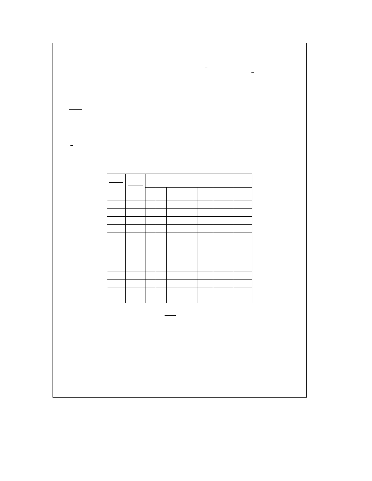
Typical K
VCO-SYNTH
Performance Characteristic
K
VCO-SYNTH
Control Register Timing Diagram
vs Data Rate
TL/F/11777– 10
FIGURE 4. MICROWIRETMCompatible Control Register Serial Load Timing Diagram
http://www.national.com 18
TL/F/11777– 4
Page 19

Detailed Block Diagram
TL/F/11777– 5
FIGURE 5a
http://www.national.com19
Page 20

AC Test Configuration
FIGURE 5b. Sample AC Test Configuration for Bench Evaluation of the DP84910
http://www.national.com 20
TL/F/11777– 6
Page 21

Control Register Description
The control register (CR) is comprised of a thirteen bit serial
shift register (eleven data bits and two address bits), four
banks of eleven bit latches and supporting logic. The latches are segmented into four subsections (banks) to allow the
user to load/reload subsets of control bits without having to
enter the entire contents of forty-four bits. Information is
strobed into the shift register via the CONTROL REGISTER
DATA (CRD) input on the positive edge of CONTROL REGISTER CLOCK (CRC) input with the CONTROL REGISTER
LATCH/SHIFT BAR (CRL/S
data from the shift register is parallel transmitted to one of
the four latch banks when CRL/S
sition. To minimize power consumption, the CRL/S
should be kept at a logical high state except when shifting
data into the control register. (When this pin is at a logical
high level, power to the shift register is interrupted.) The
SLEEP
and IDLE/SERVO pins must be disabled (SLEEP
high and IDLE/SERVOelow) in order to enter data into
the control register.
Bit positions two through twelve contain the control information. The last two bits entered into the shift register (positions zero and one) are the two address bits which select
) pin at a logical low state. The
is given a positive tran-
pin
one of the four latch banks into which the data bits are
loaded. Table IIa lists the control register bit names and
briefly describes their functions. When the device is first
powered on or the sleep mode is exited, all the information
bits are forced to Power-On-Reset (POR) states. The CONTROL REGISTER DATA OUTPUT (CRDO) pin issues data
from the shift register. This output is made available so that
it can be connected to the input of another device’s control
register input such as NSC’s ENDEC (DP84900). This will
minimize the number of data lines from the controller. Even
though all control register latches are preset into known
states when the DP84910 is energized (either by applying
V
or taking SLEEP high), the shift register flip-flops are in
CC
indeterminate states until valid data is shifted fully through
the register. Thus, the CRDO data is not valid after power
e
up until all thirteen bits have been shifted in. Also note that if
the CRL/S
input is given a positive transition after power up
occurs but before valid data has been entered into the shift
register, the indeterminate contents of the shift register will
be randomly loaded into one of the four banks of latches.
Valid data must be loaded into the shift register before
CRL/S
is given a positive transition.
FIGURE 6. Control Register Block Dlagram
TL/F/11777– 7
http://www.national.com21
Page 22

Control Register Description (Continued)
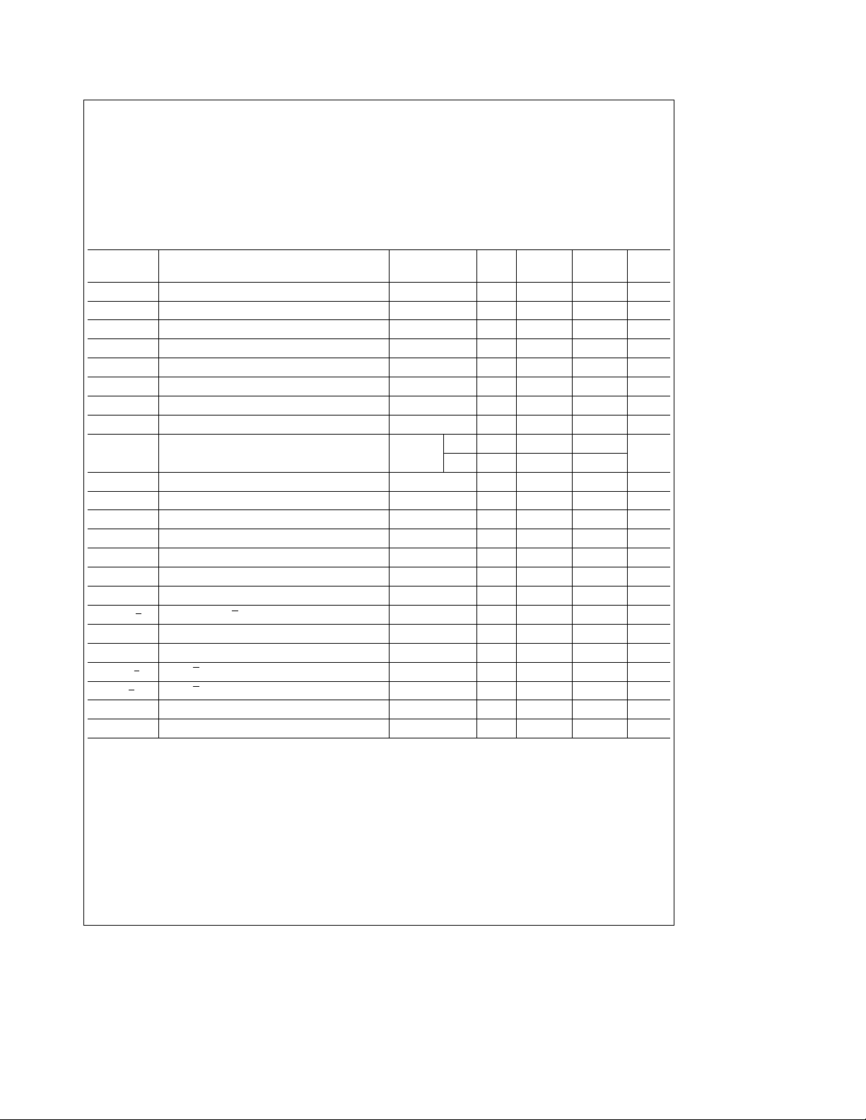
TABLE IIa. Control Register Definitions
Bit Bit Name POR Block Function
BANK (0,0)
0 CR ADDR0 CR Control Register Bank Address LSB (0)
1 CR ADDR1 CR Control Register Bank Address MSB (0)
2 FILTÐ3dBÐ0 1 FILT. Channel Filter Cutoff Frequency Selection Bit0 (LSB)
3 FILTÐ3dBÐ1 1 FILT. Channel Filter Cutoff Frequency Selection Bit1
4 FILTÐ3dBÐ2 1 FILT. Channel Filter Cutoff Frequency Selection Bit2
5 FILTÐ3dBÐ3 1 FILT. Channel Filter Cutoff Frequency Selection Bit3
6 FILTÐ3dBÐ4 0 FILT. Channel Filter Cutoff Frequency Selection Bit4
7 FILTÐ3dBÐ5 1 FILT. Channel Filter Cutoff Frequency Selection Bit5
8 FILTÐ3dBÐ6 1 FILT. Channel Filter Cutoff Frequency Selection Bit6 (MSB)
9 EQ0 1 PD Equalization Select Bit0 (LSB)
10 EQ1 0 PD Equalization Select Bit1
11 EQ2 0 PD Equalization Select Bit2 (MSB)
12 SERVO 0 PD Disable BW/EQ Control Servo Field (0eDisable)
BANK (0,1)
0 CR ADDR0 CR Control Register Bank Address LSB (1)
1 CR ADDR1 CR Control Register Bank Address MSB (0)
2 PDATA0 1 SYNTH Feedback Divider Bit0 (LSB)
3 PDATA1 0 SYNTH Feedback Divider Bit1
4 PDATA2 0 SYNTH Feedback Divider Bit2
5 PDATA3 0 SYNTH Feedback Divider Bit3
6 PDATA4 0 SYNTH Feedback Divider Bit4
7 PDATA5 0 SYNTH Feedback Divider Bit5 (MSB)
8 PDATA6 1 SYNTH Input Divider Bit0 (LSB)
9 PDATA7 0 SYNTH Input Divider Bit1
10 PDATA8 0 SYNTH Input Divider Bit2
11 PDATA9 0 SYNTH Input Divider Bit3
12 PDATA10 0 SYNTH Input Divider Bit4 (MSB)
BANK (1,0)
0 CR ADDR0 CR Control Register Bank Address LSB (0)
1 CR ADDR1 CR Control Register Bank Address MSB (1)
2 SYNCÐPWRÐDN 1 SYNC Selective Power Down of Synchronizer (Power DowneHigh)
3 STHÐPWRÐDN 1 SYNTH Selective Power Down of Synthesizer (Power DowneHigh)
4PDÐPWRÐDN 1 PD Selective Power Down of Pulse Detector (Power DowneHigh)
5 ENSTHO 1 SYNTH Enable SYNTH Output (when low)
6 GATEÐDEL1 0 PD Gating Channel Delay Select Bit 1(LSB)
7 GATEÐDEL2 1 PD Gating Channel Delay Select Bit 2(MSB)
http://www.national.com 22
Page 23

Control Register Description (Continued)
TABLE IIa. Control Register Definitions (Continued)
Bit Bit Name POR Block Function
BANK (1,0)
8 STRÐSIGN 0 SYNC Strobe Sign Bit (0epos., 1eneg.)
9 STR0 0 SYNC Strobe Bit0 (LSB)
10 STR1 0 SYNC Strobe Bit1
11 STR2 0 SYNC Strobe Bit2 (MSB)
12 CPRATIO 0 SYNC Synchronizer Charge Pump Gain Control
BANK (1,1)
0 CR ADDR0 CR Control Register Bank Address LSB (1)
1 CR ADDR1 CR Control Register Bank Address MSB (1)
2 ERD0 0 PD/SC ERD Control Bit 0 (Note 1)
3 ERD1 0 PD/SC ERD Control Bit 1 (Note 1)
4 PREAMÐ2T 0 SYNC Select 2T Preamble (3T if low)
5 INVÐWG 1 PD Select WG Polarity (1eactive low)
6 SLOW 1 PD Select 1.7 ms Delay on AMPIN (Lowe3.4 ms delay)
7 HYSÐVTH0 1 PD Hysteresis Voltage Control Bit0 (LSB)
8 HYSÐVTH1 0 PD Hysteresis Voltage Control Bit1
9 HYSÐVTH2 1 PD Hysteresis Voltage Control Bit2 (MSB)
10 SERVOÐEQ0 1 FILT Filter Bandwidth/Equalization Control-Servo Bit0 (LSB)
11 SERVOÐEQ1 1 FILT Filter Bandwidth/Equalization Control-Servo Bit1
12 SERVOÐEQ2 1 FILT Filter Bandwidth/Equalization Control-Servo Bit2 (MSB)
Note 1: When ERD0 and ERD1 are both high. the GCA is put into a fixed gain mode. The synchronizer and synthesizer are put into test modes where their VCO’s
are driven by external signals.
Pulse Detector Description
The purpose of the pulse detector is to convert the timing
information contained in the analog peaks of the disk waveform into a digital signal whose leading edge accurately represents the time position of the analog peaks.
Raw disk data from the output of an external read preamplifier is capacitively coupled to the inputs of the DP84910’s
gain controlled amplifier (AMPIN1, AMPIN2). These inputs
are switched to low impedance when the WRITE GATE input pin is enabled and stays at a low impedance for either
1.7 msor3.4ms after WRITE GATE is disabled. The amount
of delay is selectable via a bit in the control register (SLOW
Bank (1,1), bit 6). During this time, any DC offsets accumulated across the input coupling capacitors during the write
mode are removed. Also during the write mode, the AGC
voltage is held fixed and the input signal to the amplifier is
blocked. DC offsets at the output of the amplifier are the
same for read or write modes.
The gain controlled amplifier (GCA) accepts signals in the
range of 20 mV to 200 mV peak-to-peak differential and
produces a constant 500 mV peak-to-peak differential sig-
nal at the channel inputs (CHAN1, CHAN2). The channel
input signal amplitude is set by a voltage applied to the
VREF pin. There is a one-to-one correspondence between
the voltage applied to the VREF pin and the peak-to-peak
differential signal at the GCA outputs. The VREF voltage is
typically set by a voltage divider between supply and
ground. A switched supply pin (SVCC) can be used to provide the supply reference for this divider.
The gain of the GCA is controlled by a fast equal-attack,
equal decay, pattern insensitive, exponential responding,
automatic gain controlled (AGC) amplifier circuit. The AGC
,
allows for fast settling within 3 ms for a 50% change in the
input signal level. The exponential response of the AGC allows the settling time to be independent of the input signal
level. The response is pattern insensitive because the
charging or discharging of the AGC capacitor is allowed
only in the presence of a signal. Thus, large shoulder regions will not cause the AGC voltage to droop. A high impedance AGC input pin allows for an AGC hold function with
very little leakage of the AGC capacitors’ charge.
http://www.national.com23
Page 24

Pulse Detector Description (Continued)
The differentiator extracts the timing information from the
peaks of the disk signal. The timing of the peaks is preserved in the zero-crossing of the signal at the differentiator
output. A zero-cross detector is used in conjunction with the
qualification channel to provide noise free, encoded data
pulses to the data synchronizer. Fully differential circuits are
used throughout the pulse detector to minimize pulse pairing.
In order to not interpret noise on the baseline as input data,
a hysteresis comparator is used for qualifying the channel
input signal. Two pins set the hysteresis level by the application of an external voltage. One pin sets the hysteresis
level in a data field (SETHYSD) and the other pin sets the
hysteresis level in a servo field (SETHYSS). The SFIELD pin
controls the selection between these pins. A resistive divider between supply and ground is typically used to provide
these voltages. A switched supply output pin (SVCC) is
available to be used as the supply reference for these dividers. The SETHYSD voltage is adjustable in eight steps via
bits in the control register (HYSÐVTH0, HYSÐVTH1,
HYSÐVTH2, Bank (1,1) bits 7, 8, 9) (see Table IIb).
TABLE IIb. Hysteresis Threshold Control
Ctrl. Reg. Bits
HYSÐVTH2 HYSÐVTH1 HYSÐVTH0
11129
1 1 0 33.5
10138
1 0 0 42.5
01147
0 1 0 51.5
00156
0 0 0 60.5
SETHYSDe450 mV
Two bits in the control register (ERD0, ERD1, Bank (1,1)
bits 2, 3) direct the output of the pulse detector to either the
input of the data synchronizer section, the ERDOUT pin or
both (see Table III). A test mode is entered when both of
these control register bits are at a logical high level. In this
mode the GCA is put into a fixed gain mode, the VCOs are
stopped, the CRD input is redirected to act as a clock
source for the synchronizer and the CRC pin as a clock
source for the synthesizer.
TABLE III. SYNCH./PD I/O Pin Control
Ctrl. Reg.
Bank (1,1)
Pins Enabled
ERD1 ERD0 ERDOUT ERDIN
0 0 NO NO OFF
0 1 YES NO OFF
1 0 YES YES* OFF
1 1 YES YES* ON
*Internal pulse detector feed through to synchronizer is disabled; ERDIN is
input to the synchronizer.
% Qual.
Test
Mode
The pulse detector output pulse width is internally fixed to
approximately 15 ns, independent of data rate.
Four gated peak detectors are used to detect quadrature
embedded servo bursts. When gated on, the peak detector
charges an external capacitor to a DC level proportional to
the amplitude of the servo burst. The output voltage range
of these detectors is large enough for 7 bits of resolution.
The gating and discharge of the servo capacitors are controlled by five TTL level logic pins (S1, S2, S3, S4 and
HOLD) as described by Table IV. The servo channel is designed for very low servo offsets and good gain linearity.
Two servo difference amplifiers (DIFFAMP1, DIFFAMP2)
have been added to the DP84910 which were not present in
previous NSC integrated read channel circuits. The first difference amplifier (DIFFAMP1) takes the difference between
servo channel 1 (SCAP1) and channel 2 (SCAP2). The second difference amplifier (DIFFAMP2) takes the difference
between servo channel 3 (SCAP3) and channel 4 (SCAP4).
These differences are centered around an externally supplied reference voltage at the VDIFF pin. This reference
voltage is typically set at one half the supply voltage.
Two modes of servo operation are now available, track follow and seek modes. The control or selection of these
modes are with the servo switches (S1 through S4) and
HOLD pins (see Table IV). The difference between these
modes is the amount of charging time the servo peak detector needs to reach its final value, with the same input conditions. The track follow mode has a slower charge time than
the seek mode. With a slower charge time the peak detectors will be less sensitive to noise on the servo signal. Previous NSC integrated read channel devices only provided the
track follow mode.
An output internal signals mode can be entered by applying
a logical high level to the S2 pin and a logical low level to
the HOLD pin. In this mode certain selected internal signals
of the pulse detector are routed to the four servo output pins
(SCAP1–SCAP4) as observation points. These signals include the fully differential analog output of the differentiator
(SCAP1 and SCAP2 pins), the output of the zero-cross detector at the differentiator output (SCAP3 pin), and the delayed qualification signal (SCAP4 pin). This mode is useful
for the system designer while optimizing the implementation
of the pulse detector. This mode would not normally be selected in a production drive as it precludes the operation of
these pins for embedded servo use.
http://www.national.com 24
Page 25

Pulse Detector Description (Continued)
TABLE IV. Servo Control Truth Table
HOLD S1 S2 S3 S4 Function
0 0000Previously Latched Mode
0 1000Latch Track Follow Mode
0 0100Output Internal Signals and Previously Latched Mode
0 1100Output Internal Signals and Latch Track Follow Mode
0 0010Latch Seek Mode
0 1010NotAllowed
0 0110Output Internal Signals and Latch Seek Mode
0 1110NotAllowed
0 0001Discharge Servo Caps and Previously Latched Mode
0 1001Discharge Servo Caps and Latch Track Follow Mode
0 0101Discharge Servo Caps and Output Internal Signals
0 1101Discharge Servo Caps, Output Internal Signals and Latch Track Follow Mode
0 0011Discharge Servo Caps and Latch Seek Mode
0 1011NotAllowed
0 0111Discharge Servo Caps, Output Internal Signals and Latch Seek Mode
0 1111NotAllowed
1 0000Previously Latched Mode
1 1000Gate On SCAP1 and Previously Latched Mode
1 0100Gate On SCAP2 and Previously Latched Mode
1 1100Gate On SCAP1/SCAP2 and Previously Latched Mode
1 0010Gate On SCAP3 and Previously Latched Mode
1 1010Gate On SCAP1/SCAP3 and Previously Latched Mode
1 0110Gate On SCAP2/SCAP3 and Previously Latched Mode
1 1110Gate On SCAP1/SCAP2/SCAP3 and Previously Latched Mode
1 0001Gate On SCAP4 and Previously Latched Mode
1 1001Gate On SCAP1/SCAP4 and Previously Latched Mode
1 0101Gate On SCAP2/SCAP4 and Previously Latched Mode
1 1101Gate On SCAP1/SCAP2/SCAP4 and Previously Latched Mode
1 0011Gate On SCAP3/SCAP4 and Previously Latched Mode
1 1011Gate On SCAP1/SCAP3/SCAP4 and Previously Latched Mode
1 0111Gate On SCAP2/SCAP3/SCAP4 and Previously Latched Mode
1 1111Gate On SCAP1/SCAP2/SCAP3/SCAP4 and Previously Latched Mode
Channel Filter Description
The integrated channel filter is a continuous-time analog implementation of an 0.05 degree error equal ripple LC ladder
filter as shown in
sen because it has extended phase linearity and better amplitude response in the stop band when compared to other
filter types of the same order. The amount of pulse slimming
is selectable, by control register bits, in eight steps with a
maximum 9 dB of peaking. The filter’s
selectable, by control register bits, in a maximum of 128
steps. Dual
for servo field, are selectable by control register bits and
multiplexed by the SFIELD pin (when enabled by control
register bit, SERVO
altering of the channel filter bandwidth on the fly without
accessing the control register. Dual AGC control pins, one
for data field and one for servo field, insures quick settling
times when the filter bandwidth is changed in this manner. A
dedicated PLL for the channel filter is included to ensure the
Figure 8
. The equal ripple filter was cho-
b
3 dB frequency is
b
3 dB frequencies, one for data field and one
). The SFIELD pin control allows for the
filter characteristics remain independent of supply, temperature and process variations. This PLL locks to the frequency
provided at the XTLIN pin.
C1e23.86 pF C3e13.4 pF C5e10.25 pF C7e3.042 pF
e
L2
16.03 mHL4e11.81 mHL6e7.63 mHR1e2kX
TL/F/11777– 8
FIGURE 8. Equal Ripple FilterÐLC Equivalent
http://www.national.com25
Page 26

Channel Filter Description (Continued)
VPHASE Pin
The voltage on the VPHASE pin is internally generated and
controls the Q of the integrated filter. Changing the voltage
on this pin has simultaneous effects on the filter group delay, peaking and bandwidth. It is recommended that an external voltage divider (18 kX to FV
be connected to this pin. The following response equations
have been created with this divider connected. This resistor
divider does not set the voltage at this pin. It modifies the
gain and offsets the voltage at this pin.
The connection of the divider to this pin improves the filter
group delay performance, particularly at higher data rates.
Without these resistors there is a high frequency peaking of
the group delay characteristic which in turn causes excess
peaking in the magnitude characteristic, even with no boost
selected. These effects are further exaggerated at low V
and elevated temperatures.
BANDWIDTH CONTROL
The filter bandwidth is a user determined value selected
using the FILTÐ3dBÐ0–FlLTÐ3dBÐ6 control register
bits. To some extent, the filter bandwidth is also determined
by the amount of pulse slimming (peaking) desired.
Table Va lists a set of equations that yield the control register setting (i.e., the setting of the FILTÐ3dBÐ0–FILT
3dBÐ6 CR bits) for achieving a particular bandwidth (BW)
as a function of the pulse slimming control register setting
(i.e., EQ2, EQ1 and EQ0 CR bits) and the external frequency supplied to the XTLIN pin (Fx). Both BW and Fx should
be expressed in MHz. The resulting number, when converted to binary, is the correct CR setting. The binary number
listed under the CTRL REG BITS column is the EQ2, EQ1
and EQ0 CR bit setting to achieve the indicated amount of
pulse slimming in the PEAKING column of the table.
and 24 kX to ground)
CC
CC
TABLE Va. Peaking vs
Peaking CR Bits
(Data Field)
EQ2 EQ1 EQ0
1 1 1 0.40
1 1 0 1.16
1 0 1 1.93
1 0 0 3.00
0 1 1 4.04
Ð
0 1 0 5.25
0 0 1 6.22
0 0 0 8.13
Note 1. Data Field, V
is the XTLIN input frequency (both are expressed in MHz).
F
X
CC
b
3 dB Frequency Equations
b
b
BW
b
0.016450F
b
BW
b
0.017828F
b
BW
b
0.018727F
b
BW
b
0.020077F
b
BW
b
0.021422F
b
BW
b
0.022887F
b
BW
b
0.024363F
b
BW
b
0.026331F
3 dB Equation
(Note 1)
a
X
a
X
a
X
a
X
a
X
a
X
a
X
a
X
a
x
0.051574
a
X
0.048271
a
X
0.048455
a
X
0.052433
a
X
0.059365
a
X
0.066185
a
X
0.074151
a
X
0.086751
2.1751F
2.3675F
2.4876F
2.6678F
2.8403F
3.0278F
3.2147F
3.4594F
4.8720
4.4670
4.3786
4.8513
5.6269
6.4295
7.3136
8.7398
Peaking
(dB)
e
5V, Te25§C. BW is the desired bandwidth and
The resolution of the frequency control DAC is dependent
on the frequency input at the XTLIN pin and the amount of
pulse slimming selected. Table Vb lists equations that describe the resolution of the frequency control DAC in
MHz/step. Fx
e
XTLlN frequency is expressed in MHz.
TABLE Vb. Peaking vs DAC Resolution
Peaking CR Bits
(Data Field)
EQ2 EQ1 EQ0
1 1 1 0.016450F
1 1 0 0.017828F
1 0 1 0.018727F
1 0 0 0.020077F
0 1 1 0.021422F
0 1 0 0.022887F
0 0 1 0.024363F
0 0 0 0.026331F
Note 1. Data Field, V
MHz.
e
CC
DAC Resolution Equations
(Note 1)
b
0.051574
X
b
0.048271
X
b
0.048455
X
b
0.052433
X
b
0.059365
X
b
0.066185
X
b
0.074151
X
b
0.086751
X
5V, Te25§C, FXis the XTLIN input frequency in
http://www.national.com 26
Page 27

Channel Filter Description (Continued)
PULSE SLIMMING CONTROL
As in previous NSC integrated read channel circuits, pulse
slimming is implemented using the Kost technique. Pulse
slimming operates by injecting current internal to the filter
which is 180 degrees out of phase with the GCA drive current to the filter’s inputs. The injected current has the effect
of peaking the high frequency response of the filter without
affecting the filter’s group delay characteristic. The control
register selection for different levels of peaking is shown in
Table Va.
TABLE Vc. Servo Field Peaking vs
b
3 dB Frequency Equations
Peaking CR Bits
(Servo Field)
Servo Servo Servo
Peaking
(dB)
EQ2 EQ1 EQ0
1 1 1 0.40
1 1 0 1.16
1 0 1 1.93
1 0 0 3.00
0 1 1 4.04
0 1 0 5.25
0 0 1 6.22
0 0 0 8.13
Note 1: V
XTLIN input frequency (both are expressed in MHz). SEQ2
EQ2, etc.
e
5V, Te25§C. BW is the desired bandwidth and FXis the
CC
SERVO BANDWIDTH CONTROL
The DP84910 has the ability to reduce theb3 dB frequency
and peaking characteristic of the filter without addressing
the control register. This feature is enabled by a bit in the
control register (SERVO
, Bank (0,0) bit 12) and controlled
by the SFIELD pin. This feature is desirable because the
b
b
BW
b
0.007341F
b
BW
b
0.009182F
b
BW
b
0.014272F
b
BW
b
0.016692F
b
BW
b
0.017666F
b
BW
b
0.018543F
b
BW
b
0.019883F
b
BW
b
0.020475F
3 dB Equation
(Note 1)
a
X
X
a
X
X
a
X
X
a
X
X
a
X
X
a
X
X
a
X
X
a
X
b
x
0.000213
a
0.010845
a
0.050838
a
0.059598
a
0.054288
a
0.049550
a
0.055912
a
0.053289
e
1.0368F
1.2651F
1.8836F
2.1728F
2.3386F
2.4648F
2.6334F
2.7258F
0.4774
0.5037
5.0496
5.5646
5.1777
4.5824
5.1666
4.9201
SERVO
servo field is often written at a lower frequency than the
data field. Reducing the bandwidth for a servo field will maximize the servo signal-to-noise ratio.
A side effect of the Kost pulse slimming technique is that
b
the
3 dB frequency of the filter moves as the amount of
pulse slimming is changed. This property is used to advantage to reduce the channel filter bandwidth in a servo field,
by decreasing the amount of pulse slimming. If we define a
ratio (K) of the injected slimming signal to the signal at the
input of the filter we find that for values of K less the 0.2
there is no peaking in the filter magnitude response. In the
data field (i.e., SFIELD
below 0.2, even when no pulse slimming is selected (i.e.,
e
EQ2
EQ1eEQ0e1). This is illustrated in Table VI
which shows the
e
low), K is never allowed to go
b
3 dB bandwidth of the channel filter as a
function of peaking. Table VI shows that peaking in the data
field is achieved by increasing K above the minimum 0.2
level. However, if control register bit SERVO
e
1 and the
SFIELD pin is high (i.e., in a servo field) then K is allowed to
go to zero.
TABLE VI. Pulse Slimming Control Table: Data Field
Peaking CR Bits
(Data Field) (Note 1)
EQ2 EQ1 EQ0
K
Peaking
(dB)
b
3dB
BW
(MHz)
Gain
(dB)
1 1 1 0.22 0.40 18.23 6.000
1 1 0 0.28 1.16 20.60 5.450
1 0 1 0.34 1.93 21.96 4.840
1 0 0 0.41 3.00 23.37 4.200
0 1 1 0.48 4.04 24.55 3.490
0 1 0 0.55 5.25 25.84 2.730
0 0 1 0.62 6.22 27.12 1.886
0 0 0 0.69 8.13 28.52 0.956
Note 1: This table is referenced to a 10 MHz, 7 pole, 0.05 degree equal
ripple filter. V
e
CC
5V, Te25§C.
In the servo field, control register bits SERVOÐEQ2,
SERVOÐEQ1 and SERVOÐEQ0 are mulitiplexed with the
control register bits EQ2, EQ1 and EQ0, to allow for separate control of the amount of filter peaking and consequently, separate control of the filter bandwidth. Table VII shows
the effect these control register bits have on the filter bandwidth and peaking. Notice that corresponding values of K
are 0.2 less in Table VII vs. Table VI. The multiplexing action
is controlled by the SFIELD pin if control register bit SERVO
e
1.
Ð
The base frequency gain of the channel filter changes as a
function of the peaking. In order to reduce AGC settling time
when multiplexing in different levels of peaking between the
servo and data fields, a second AGC control pin (VAGCINS)
has been added. The SFIELD pin switches control between
the VAGCIND and the VAGCINS pins. This switching will
occur independent of the state of the SERVO
control regis-
ter bit.
http://www.national.com27
Page 28

Synchronizer Description (Continued)
TABLE VII. Pulse Slimming Control Table: Servo Field
Peaking CR Bits
(Servo Field) (1)
SERVO SERVO SERVO
EQ2 EQ1 EQ0
1 1 1 0.00 0.00 10.00 6.000
1 1 0 0.04 0.00 10.89 5.450
1 0 1 0.13 0.00 14.50 4.840
1 0 0 0.18 0.32 16.54 4.200
0 1 1 0.23 0.95 18.46 3.490
0 1 0 0.27 1.76 20.26 2.730
0 0 1 0.32 2.47 21.59 1.886
0 0 0 0.37 3.62 22.78 0.956
Note: This table is referenced to a 10 MHz, 7 pole, 0.05 degree equal ripple
filter. SEQ2
When either the VAGCIND or VAGCINS pin is not selected,
the filter is placed into an AGC hold mode. Because of this,
the AGC capacitors tied to the VAGCIND and VAGCINS
pins remember the correct voltage (and corresponding amplifier gain) for their respective fields. Thus the channel filter
can have different gains (as a result of different levels of
peaking) in the servo and data fields, without the penalty of
waiting for AGC settling time when the part is rapidly
switched between these two fields.
Separate AGC control pins also allow for different AGC time
constants between the servo and data fields. Typically, prior
to the servo bursts, an AGC normalization field is written.
This normalization field allows the servo AGC to adjust the
servo channel gain to a constant level independent of the
position of the read head. In order to minimize the disk
space consumed for this function, the normalization field is
usually only several microseconds long. Thus a fast AGC
time constant is typically used in the servo field to quickly
acquire the level of the normalization field.
The VAGCIND and VAGCINS pins can be tied together in
the event that separate AGC time constants are not desired
and the servo channel filter bandwidth reduction feature is
not used. This would save one external component by eliminating one of the AGC capacitors.
e
SERVOÐEQ2 etc.
K
Peaking
(dB)
b
3dB
BW
(MHz)
Gain
(dB)
Synchronizer Description
The DP84910 data synchronizer consists of a phase locked
loop (PLL) employing a delay line, a pulse gate, a phase
frequency comparator, an analog charge pump, an external
passive loop filter, a voltage controlled oscillator (VCO), and
supporting logic. The synchronizer extracts the code rate
clock from the peak detected disk data, generates bit
frames (windows) for bit capture, and reissues phase-stabilized data. The synchronization window (with strobe setting
at nominal, M
read data (ERD) pulses via the 50% duty cycle of the VCO
and the time averaging action of the PLL.
The synchronizer incorporates a zero-phase-start (ZPS)
block to minimize the phase step seen at the beginning of a
lock sequence. Prior to the beginning of a read operation,
the synchronizer PLL is locked to the output of the synthe-
e
0 position) is centered about the encoded
sizer to maintain the VCO frequency at the operating code
rate. Following READ GATE assertion, the ZPS block
freezes the synchronizer VCO and restarts it coincidentally
with disk data bit. Once the ZPS event is completed, the
SCLK output multiplexer is allowed to switch (without glitches) from its synthesizer reference to the synchronizer reference. Also, if frequency lock is employed (FLC
er is incorporated in the VCO feedback path corresponding
to the 2T or 3T sync field being used. This divider is synchronously dropped out and the pulse gate enabled once
the FLC
input is taken to a high logical level (see
Semiconductor Mass Storage Handbook
AN-414, for a discussion of frequency lock). If frequency
lock is not employed, the pulse gate becomes active immediately at the end of the ZPS sequence.
When READ GATE is disabled, ZPS is momentarily held-off
as the SCLK output multiplexer switches from transmission
of the synchronizer reference to the synthesizer reference.
Once the multiplexer switching is complete, ZPS is enabled
and the synchronizer relocks to the synthesizer reference.
(The accuracy of the VCO restart phase alignment at RG
deassertion is less stringent than when entering a read operation.)
Note that the SCLK output transmits the synchronizer clock
only after ZPS is completed when entering the read mode,
and deselects the synchronizer clock prior to the occurrence of ZPS when exiting the read mode. This makes the
ZPS event invisible to the SCLK output.
The synchronizer provides two pins for PLL filtering purposes, CHARGE PUMP OUTPUT (CPO) and VCO INPUT
(VCOI), permitting the use of high-order, two-port filters for
optimization of PLL lock characteristics and bit jitter rejection. For basic applications, CPO and VCOI may be tied
together (single-node) and a simple lead-lag, C
filter tied between these pins and ground.
The synchronizer may be selectively powered-down at the
user’s option via a single bit in the control register (SYNC
PWRÐDN, Bank (1,0) bit 2). When selective power-down
occurs within the synchronizer, an idle-biasing circuit is activated at the CPO pin which will keep the filter voltage at 2
times V
order to minimize lock recovery time at the enabling of power. When selective powering occurs, as when V
occurs, all synchronizer logic is set into the non-read mode
and the CPO idle-bias circuit is disabled.
The synchronizer pulse gate is partitioned into two sections;
the SYNC DATA bit latch and the VCO gate. The bit latch,
operating independently of the VCO gate, generates the
data synchronization window at the code clock rate based
on the 50% duty cycle of the synchronizer VCO clock. 50%
duty cycle symmetry in the VCO (or code) clock is produced
by division of a 2X oscillator signal by a differential ECL
toggle flip-flop. This symmetry-based technique eliminates
reliance on the absolute value of the delay line for nominal
window centering. The on-chip half-cell silicon delay line is
employed in conjunction with the VCO gate to align the
phase detector window (retrace angle). The delay magnitude will track the synthesizer VCO and thus any recording
data rate variations automatically, and because it is referenced to an external frequency source, it is insensitive to
external component tolerance, supply voltage, temperature,
and IC process variations.
(approximately 1.5V) above ground potential in
BE
low), a divid-
National
, Application Note
(RaC)
ll
power-up
CC
Ð
http://www.national.com 28
Page 29

Synchronizer Description (Continued)
FIGURE 10. Digital Phase-Frequency Comparator
The synchronizer employs a digital phase comparator (nonharmonic frequency discriminator) which, when frequency
lock is enabled, will force the frequency of the VCO toward
the frequency of the reference input regardless of the magnitude of the frequency difference. The function of the
phase comparator circuit can be represented in the simplified form of
Figure 10
. The AND reset path has sufficient
delay added to eliminate any ‘‘dead-zone’’ in the phase detector transfer function. The DP84910 also provides an
AGC HOLD/COAST control input (HOLD) which, during the
read mode, disables charge pump action. This function is
made available to allow the PLL to be set to free-run, undisturbed, during servo bursts or while a detectable defect is
being read from the media. External data controller circuitry
is responsible for the detection of the servo burst or defect
and for issuing the HOLD command to the DP84910.
The charge pump is a digitally gated, bidirectional current
source with selectable gain whose current flow is regulated
by the digital phase comparator circuit. The net current at
the CHARGE PUMP OUTPUT (CPO) pin reflects the magnitude and sign of the phase error seen at the input of the
phase comparator. The transfer function from the phase
comparator input to the charge pump output has a sawtooth characteristic which is linear from
(harmonic) mode, or monotonically extends to the operating
limit of the VCO in frequency (non-harmonic) mode. The
CPO pin is connected externally to a filter network whose
impedance translates the aggregate charge pump current
into a voltage for the VCO INPUT (VCOI) while providing a
low-pass filter function for the PLL. The matched sourcing
and sinking current generators’ operating currents are set
via the RNOM pin, which is connected to an external resistor whose opposite terminal is connected to ground. The
RNOM pin will self-bias to one V
be made to switch at the assertion of an internal lock detect
. Charge pump gain can
BE
signal by a selectable factor. The charge pump gain options
are selected via a bit in the control register (CPRATIO, Bank
(1,0) bit 12) and the CPGAIN pin (see Table VIII). ‘‘K1’’ refers to the absolute value of amplification of current between the RNOM and the CPO pins when either sourcing or
sinking action is gated-on. It is recommended the charge
pump operating current be kept as high as practical (using
the minimum R
programmable CP gain). This minimizes the resulting imped-
value and selecting the higher values of
NOM
ance of the loop filter for any given application, maximizing
environmental noise immunity.
TL/F/11777– 9
b
q toaq in phase
TABLE VIII. CPGAIN Control
Control
Register Bit
CPRATIO
CPGAIN
Pin
K1
008
014
108
112
The synchronizer VCO is a fully integrated oscillator (no external components) whose frequency is an exponential
function of the voltage at the VCOI pin. The VCO block
contains a 2X oscillator (two times the media code clock
rate) which is divided by two by differential ECL logic in
order to produce the necessary 50% duty cycle (code rate)
recovered clock waveform for window generation. The exponential VCO transfer characteristic produces a VCO gain
which is directly proportional to data rateÐwhile at any single operating frequency the VCO gain characteristic closely
approximates linear behavior (see
Technical Papers
, ‘‘A 33 Mb/s Data Synchronizing Phase-
1988 ISSCC Digest of
Locked Loop’’, for a discussion of an exponential gain VCO
in data recovery applications). The data rate dependency of
loop gain causes the PLL bandwidth to track recording data
rate variations (BW varies with the square root of the gain).
The synchronizer VCO control block employs a positivesense feed-forward bias signal derived from the synthesizer
which forces the VCOI pin to remain at a relevantly constant
voltage independent of data rate. This can give the misleading impression that a very high synchronizer VCO gain exists if the synchronizer VCO frequency is varied coincidentally with the synthesizer VCO. Gain of the synchronizer
VCO must only be measured with the synthesizer frequency
held constant in order to prevent the bias normalization circuitry from effecting the VCOI bias point.
The SCLK pin is provided so that an external encoder/decoder (ENDEC) can use the VCO clock from either the synchronizer (read mode) or synthesizer (non-read mode). The
multiplexer switches from synthesizer VCO to synchronizer
VCO only after ZPS occurs when entering the read mode
and, when exiting the read mode, switches back to the synthesizer VCO prior to the occurrence of ZPS. All multiplexing is done with no glitches.
Thirteen position window strobing (nominal position and 6
steps on either side of center) is available via the control
register (see Table IX). Strobing on either side of nominal is
achieved via a patented technique which modulates the
window position without any disturbance of the PLL’s phase
equilibrium or movement of the retrace angle. In addition,
strobe response is immediate, requiring no settling time.
The first two positions on either side of nominal (M
b2,a
1, ora2) are fixed-delay steps of approximately
eb
0.6 ns each (see AC Electrical Characteristics table), intended for fine-stepping functions such as window deskewing.
All remaining steps (
b
3 throughb6 anda3 througha6)
are equal and dependent on data rate, each step being one
sixteenth (6.25%) of the window width.
1,
http://www.national.com29
Page 30

Synchronizer Description (Continued)
TABLE IX. Window Strobe Control Table
Control Register Bits Bank (1,1)
STR2 STR1 STR0 STRÐSIGN Typical Window Shift
110 1
101 1
100 1
011 1
010 1
001 1
b
(0.250)t
b
(0.188)t
b
(0.125)t
b
(0.062)t
VCO
VCO
VCO
VCO
b
1.2 ns
b
0.6 ns
b
b
b
b
1.2 ns
1.2 ns
1.2 ns
1.2 ns
0 0 0 1 none
0 0 0 0 none
0 0 1 0 0.6 ns
0 1 0 0 1.2 ns
0 1 1 0 (0.062)t
1 0 0 0 (0.125)t
1 0 1 0 (0.188)t
1 1 0 0 (0.250)t
Note: Strobe selections not shown in above table are invalid and should not
be used. If an invalid state is inadvertently entered, SDO will become indeterminate, though PLL lock (phase comparator activity) will not be affected.
VCO
VCO
VCO
VCO
a
a
a
a
1.2 ns
1.2 ns
1.2 ns
1.2 ns
Synthesizer Description
The synthesizer block is a phase-locked loop with control
register selectable divider values at its input port and in its
feedback path. A single, external node (Timing Extractor Filter, or TEF) is provided for passive components for the syn-
thesizer PLL filter. The resulting synthesized output, f
is the code rate clock used for encoding and as a reference
signal for the synchronizer during the non-read mode. The
frequency of f
plied by the modulus of the feedback divider and divided by
is the reference input frequency multi-
SYNTH
the modulus of the input divider:
c
e
f
SYNTH
The input divider modulus N
Bank (0,1), bits 8 –12 (LSB –MSB, respectively), and feed-
f
REF
N
feedback/Ninput
is set via control register
input
SYNTH
back modulus N
(0,1), bits 2 –7 (LSB –MSB, respectively). The value of each
is set via control register Bank
feedback
N modulus is equal to the binary value of its control word
PLUS 2. This gives the input divider a division range of 3 –33
and the feedback divider a division range of 3 –65.
e
[
N
N
Binary value of CR Bank (0,1), bits 8–12
input
e
[
feedback
Binary value CR Bank (0,1), bits 2–7
A zero value control word (all bits low) for either divider is
not allowed (divider operation stops). At V
divider control words are both automatically set to binary 1,
and thus the ratio:
N
feedback/Ninput
e(1a
2)/(1a2)e(3)/(3), or unity.
The synthesizer may be selectively powered-down via a single bit in the control register (STHÐPWRÐDN, Bank (1,0)
bit 3). No control register data is lost during selective powerdown. When selective power-down occurs, an idle-bias circuit is activated at the TEF pin which keeps the filter voltage
at a typical operating bias of 2 times V
1.5V) above ground potential in order to minimize lock recovery time at reapplication of power.
Note: The synchronizer derives key reference signals from the synthesizer;
thus, the synthesizer must be powered-on for the synchronizer to
operate properly. If the synthesizer is powered-down, the synchronizer should be as well.
In general, to minimize digital switching noise, it is advised
that the SYNC CLOCK (SCLK) output be used for all read/
write clock purposes and the SYNTH output be left disabled. For systems which must use a continuous, unmultiplexed, synthesized master clock, the SYNTH output is
made available. Should the SYNTH output be employed as
a system clock, care should be taken, as with all switching
outputs on the DP84910, to minimize capactive loading (use
an external buffer/driver for multiple fan-out applications).
The standard, default V
SYNTH output pin is the disabled mode (logic high state).
power-up condition for the
CC
This output should always be left disabled if not needed.
,
power-up, the
CC
(approximately
BE
a
]
2
a
]
2
http://www.national.com 30
Page 31

http://www.national.com31
Page 32

Physical Dimensions inches (millimeters) unless otherwise noted
DP84910 (-36/-50) Integrated Read Channel
Order Number DP84910VHG-36 or DP84910VHG-50
80-Pin PQFP Package
NS Package Number VHG80A
LIFE SUPPORT POLICY
NATIONAL’S PRODUCTS ARE NOT AUTHORIZED FOR USE AS CRITICAL COMPONENTS IN LIFE SUPPORT
DEVICES OR SYSTEMS WITHOUT THE EXPRESS WRITTEN APPROVAL OF THE PRESIDENT OF NATIONAL
SEMICONDUCTOR CORPORATION. As used herein:
1. Life support devices or systems are devices or 2. A critical component is any component of a life
systems which, (a) are intended for surgical implant support device or system whose failure to perform can
into the body, or (b) support or sustain life, and whose be reasonably expected to cause the failure of the life
failure to perform, when properly used in accordance support device or system, or to affect its safety or
with instructions for use provided in the labeling, can effectiveness.
be reasonably expected to result in a significant injury
to the user.
National Semiconductor National Semiconductor National Semiconductor National Semiconductor
Corporation Europe Hong Kong Ltd. Japan Ltd.
1111 West Bardin Road Fax:
Arlington, TX 76017 Email: europe.support@nsc.com Ocean Centre, 5 Canton Rd. Fax: 81-043-299-2408
Tel: 1(800) 272-9959 Deutsch Tel:
Fax: 1(800) 737-7018 English Tel:
http://www.national.com
National does not assume any responsibility for use of any circuitry described, no circuit patent licenses are implied and National reserves the right at any time without notice to change said circuitry and specifications.
Fran3ais Tel:
Italiano Tel:a49 (0) 180-534 16 80 Fax: (852) 2736-9960
a
49 (0) 180-530 85 86 13th Floor, Straight Block, Tel: 81-043-299-2308
a
49 (0) 180-530 85 85 Tsimshatsui, Kowloon
a
49 (0) 180-532 78 32 Hong Kong
a
49 (0) 180-532 93 58 Tel: (852) 2737-1600
 Loading...