

Page 1
DP84902
1,7 Encoder/Decoder Circuit
General Description
The DP84902 is designed to perform the encoding and decoding for disk memory systems. It is designed to interface
directly with Integrated Read Channel Products (such as
National Semiconductor’s DP84910) and with Disk Data
Controller Products with a 2-bit NRZ interface (such as National Semiconductor’s Advanced Disk Controllers). This
Encoder/Decoder (ENDEC) circuit employs a 2/3 (1,7) Run
Length Limited (RLL) code type and supports the hard sectored format.
The DP84902 has the option of selecting either TTL or ECL
compatible code output to interface with preamplifiers commonly used in high data rate applications. This is accommplished by the setting of a bit in the control register.
The ENDEC also includes write data precompensation control circuitry which detects the need for write precompensation. This circuitry issues early and late output signals necessary for precompensation. The precompensation information is generated against a 2T pattern. The precompensation circuitry can be bypassed by the setting of a bit in the
control register.
A control reigster is included to configure the ENDEC and to
select device operation options such as output code inversion, differential code output, bypassing of the encoder, and
the use of an internal write clock.
June 1994
The DP84902 is available in 20-pin SO and 20-pin SSO
packages.
Features
Y
Operates at 2-bit Non-Return to Zero (NRZ) Data Rates
up to 50 Mbits/second
Y
Singlea5V Power Supply Operation
Y
Low Power Dissipation when TTL compatible code output is selected. 150 mW at 50 Mbits/second NRZ Rate
Y
TTL Compatible Inputs and Outputs
Y
ECL Compatible Code Outputs (patented) are control
register selectable
Y
Two-bit NRZ Interface
Y
Supports Write Data Precompensation with Early and
Late output signals
Y
Selectable use of either an Internal or External Write
Clock
Y
Power Down Mode Included
Y
DC-Erasure is available to support Analog Flaw Mapping Testing
Y
Bypass Mode available which permits Un-Encoded Test
Patterns to be issued at the CODEOUT Pin
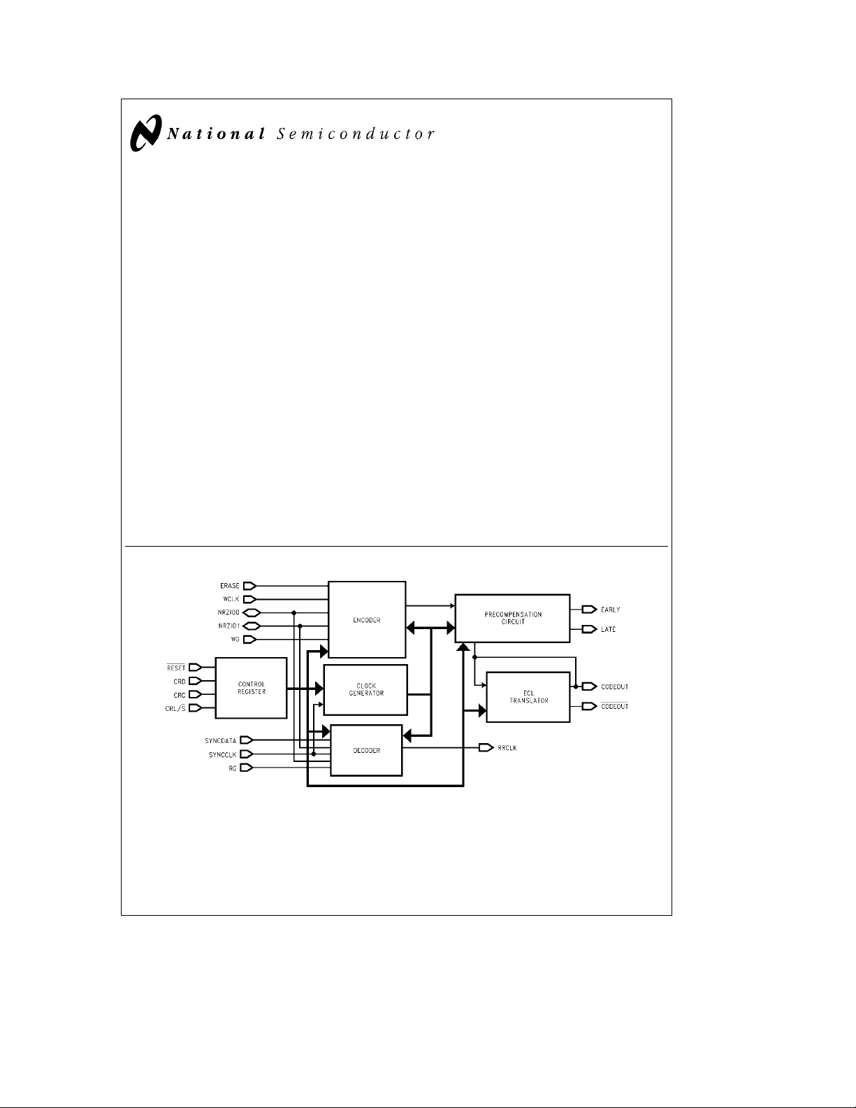
DP84902 1,7 Encoder/Decoder Circuit
Block Diagram
FIGURE 1. DP84902 ENDEC Block Diagram
TRI-STATEÉis a registered trademark of National Semiconductor Corporation.
IBM
is a registered trademark of International Business Machines Corporation.
É
C
1995 National Semiconductor Corporation RRD-B30M105/Printed in U. S. A.
TL/F/11963
TL/F/11963– 1
Page 2
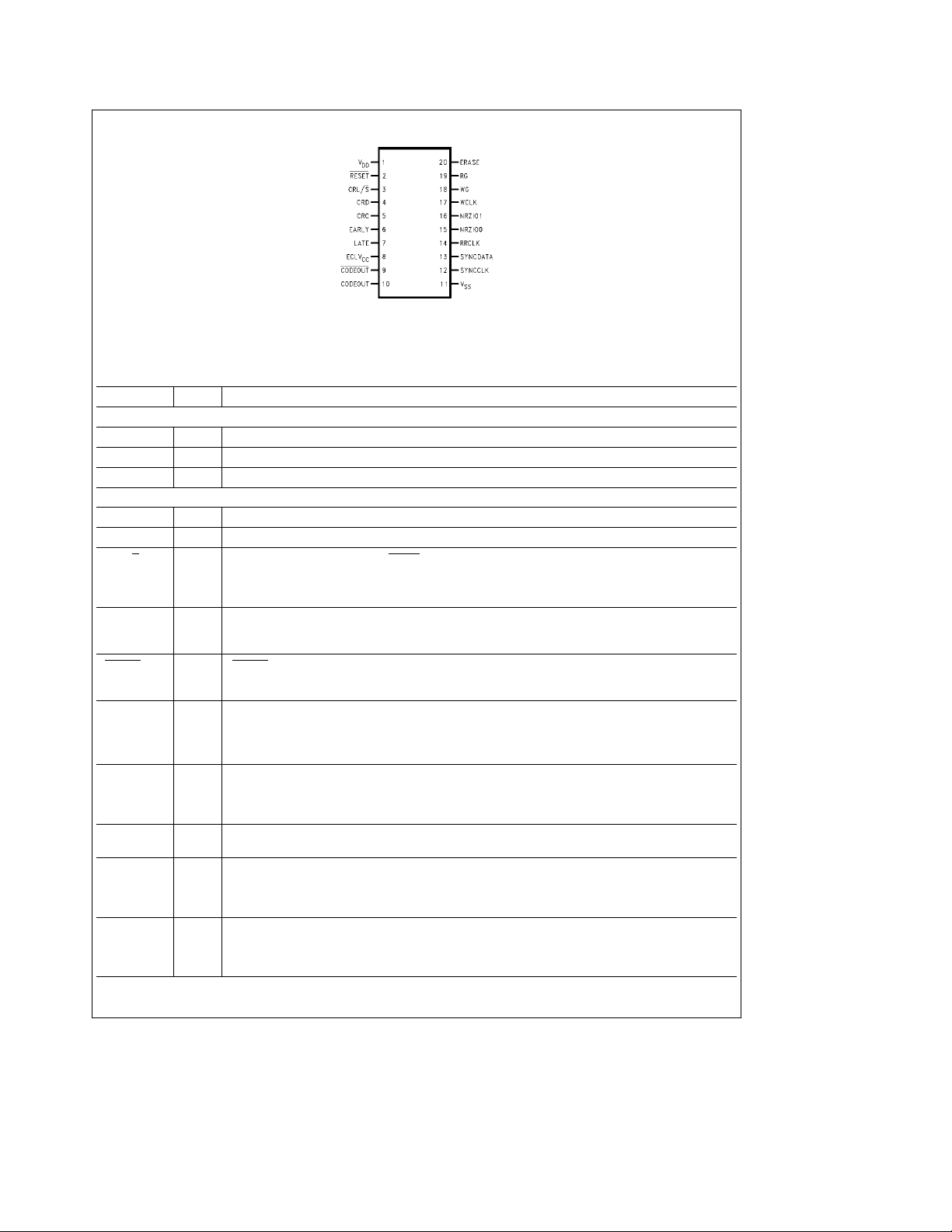
Connection Diagram
FIGURE 2. DP84902 Pinout
Order Number DP84902M or DP84902MS
See NS Package Number M20B or MSA20
TL/F/11963– 2
Pin Descriptions
Symbol Pin
Power Supply and Ground Pins
ECLV
CC
V
DD
V
SS
Input Pin Descriptions
CRC 5 CONTROL REGISTER CLOCK: Positive-edge-active control register clock input.
CRD 4 CONTROL REGISTER DATA: Control register data input
CRL/S 3 CONTROL REGISTER LATCH/SHIFT: A logical low state applied to this input allows the CONTROL
ERASE 20 ERASE: This active high input is used while in the write mode to force a logical low at the CODEOUT
RESET 2 RESET: A logical low level applied to this input forces the ENDEC to a power-on-reset state, and
RG 19 READ GATE: This input accepts a mode control signal from the controller for the decoder. It permits
SYNCCLK 12 SYNCHRONIZED CLOCK: This input accepts the code rate (1.5F) synchronized clock signal from the
SYNCDATA 13 SYNCHRONIZED DATA: This input accepts the synchronized data signal, MSB first, from the read
WCLK 17 WRITE CLOCK: This input is used only in the external write clock mode. The write clock signal (Note 1)
WG 18 WRITE GATE: This input accepts a mode control signal from the controller for the encoder. It permits
Ý
8 ECLVCCSupply Pin: 5Vg10%
1VDDSupply Pin: 5Vg10%
11 VSS: Ground reference
REGISTER CLOCK input to clock data into the control register’s shift register via the CONTROL
REGISTER DATA input. A logical high state latches the data into a bank of latches and issues the
information to the appropriate circuitry within the ENDEC.
output (or a logical high if CODEOUT is inverted). This is useful to blank out (DC erase which issues no
transitions) a track for analog flaw map tesing.
presets its control register to predetermined operating setup conditions. During normal operation, this
pin must be held at a logical high level.
the reading of data from the disk when at a logical high level. It inhibits reading and resets the decoder
state machine when at a logical low level. There are no set-up or hold timing requirements for the
enabling or disabling of this input.
read channel’s data synchronizer. This signal is used to clock the synchronized data into the decoder
on the negative edge of SYNCCLK in the read mode and is the source clock for clocking codeout data
from the encoder during the write mode.
channel’s data synchronizer for the decoder’s use.
from the controller is used to strobe the NRZ input data into the ENDEC. The write clock signal from the
controller must be the RRCLK echoed by the controller. If the external write clock mode is not selected,
this pin should be tied to V
the writing of a header and data to the disk when at a logical high level. It inhibits writing and resets the
encoder state machine when at a logical low level. There are no set-up or hold timing requirements for
the enabling or disabling of this input.
DD
or VSS.
Functional Description
2
Page 3
Pin Descriptions (Continued)
Symbol Pin
Output Pin Descriptions
CODEOUT 10 (1,7) RLL CODE OUTPUT: This output issues encoded data, MSB first, to be written to the disk. The
CODEOUT 9 (1,7) RLL COMPLEMENTARY CODE OUTPUT: This output is the complement of the ECL differential
EARLY 6 EARLY PRECOMPENSATION OUTPUT: This pin is the early precompensation output. It issues a logical
LATE 7 LATE PRECOMPENSATION OUTPUT: This pin is the late precompensation output. It issues a logical
RRCLK 14 READ/REFERENCE CLOCK: This output issues read clock to the controller at all times (Note 1). This
Input/Output Pin Descriptions
NRZIO0 15 LEAST SIGNIFICANT BIT NRZ INPUT/OUTPUT: This I/O pin represents the Least Significant Bit
NRZIO1 16 MOST SIGNIFICANT BIT NRZ INPUT/OUTPUT: This I/O pin represents the Most Significant Bit (MSB)
Note 1: With the code rate at 1.5F, the effective NRZ data rate is 1F. Since this chip employs a 2-bit NRZ interface, the write (WCLK) and read/reference (RRCLK)
clocks are 0.5F.
Ý
control register controls various attributes of this output. It can be configured either as a TTL or ECL
compatible output. In the TTL mode, the sense of the output can be selectively inverted to allow the
active edge to be either the positive or negative transition and can also be put into a high impedance
state (TRI-STATE
precompensation circuitry can be bypassed. The encoder can also be bypassed thus permitting uncoded
test patterns to be issued from this pin.
CODEOUT output pin. It issues encoded data to be written to the disk. It is enabled as an ECL output by
a control register bit. If the TTL mode is selected (by a control register bit), this pin will be in a high
impedance state (TRI-STATE).
high level to indicate that early precompensation is needed. This signal is used by National
Semiconductor Integrated Read Channel Products, such as the DP8492, to precompensate the final
coded data before it goes to the read/write circuit.
high level to indicate that late precompensation is needed. This signal is used by National
Semiconductor Integrated Read Channel Products, such as the DP8492, to precompensate the final
coded data before it goes to the read/write circuit.
signal is used to clock decoded NRZ data into the controller in the read mode (READ CLOCK) and is to
be echoed back to the ENDEC by the controller in the write mode for use as a write clock (REFERENCE
CLOCK) if external write clock mode is selected in the control register.
(LSB) of NRZ data. As an input, it accepts the NRZ LSB data signal from the controller. Data is strobed
into the ENDEC on the positive-edge of the WRITE CLOCK (if external write clock mode is selected in
the control register), encoded and written to the disk in (1,7) format. This NRZ input must be low while
the preamble and address mark fields are being written. This pin is also used to transfer un-encoded test
patterns to the CODEOUT pin. As an output, it issues the decoded NRZ LSB data to the controller during
a read operation. NRZ output data will be clocked into the controller on the positive-edge of the READ/
REFERENCE CLOCK (RRCLK).
of NRZ data. As an input, it accepts the NRZ MSB data signal from the controller. Data is strobed into
the ENDEC on the positive-edge of the WRITE CLOCK (if external write clock mode is selected in the
control register), encoded, and written to the disk in (1,7) format. This NRZ input must be held low while
the preamble and address mark fields are being written. As an output, this pin issues the decoded NRZ
MSB data to the controller during a read operation. The decoded NRZ output data will be clocked into
the controller on the positive-edge of the READ/REFERENCE CLOCK (RRCLK).
) which allows the multiplexing of this pin with another device or pin. The
É
Functional Description
3
Page 4
DC and AC Device Specifications
Absolute Maximum Ratings
Note: Absolute Maximum Ratings are those values beyond which the safety
of the device cannot be guaranteed. The device should not be operated at these limits. The parametric values defined in the ‘‘Electrical
Characteristics’’ tables are not guaranteed at these ratings. The ‘‘operating conditions’’ table will define the conditions for actual device
operation.
(Note)
Supply Voltage ААААААААААААААААААААААААААААААААААААА7V
TTL Input Maximum Voltage ААААААААААААААААААААААААА7V
Maximum Output Voltage АААААААААААААААААААААААААААА7V
ESD Susceptibility (Note 1) ААААААААААААААААААААААА2000V
Note 1: Human Body model used. (100 pF through 1.5 kX)
General Operating Conditions are guaranteed over supply voltage and operating ambient temperature
ranges unless otherwise specified.
Symbol Parameter Min
VDD, ECLV
T
A
T
S
C
LOAD
Supply Voltage 4.5 5 5.5 V N/A
CC
Operation Ambient Temperature 0 70
Storage Temperature
b
Capacitive Load on any Output ECL Output 10
TTL Output 15
I
OH
I
OL
V
IH
V
IL
f
NRZ
f
SCLK
t
PW(RESET)
t
PW(RG, WG)
Note 1: Typical values are specified at 25§C and 5V supply.
Note A: This parameter is guaranteed by outgoing testing.
Note B: The limit values have been determined by characterization data. No outgoing tests are performed.
High Logic Level Output Current
(CMOS Logic Outputs Only)
Low Logic Level Output Current EARLY, LATE 6
(CMOS Logic Outputs Only)
All Others 8 (Note A)
High Logic Level Input Voltage 2 V (Note A)
Low Logic Level Input Voltage 0.8 V (Note A)
NRZ Transfer Rate Operating Frequency 5 50 Mb/s (Note A)
SYNCCLK Operating Frequency 7.5 75 MHz (Note A)
RESET Pulse Width (negative)
(See
Figure 3
) PERIODS
5
RG or WG Wait Time after Power Down or Reset
with Respect to Positive Edge of CRL/S
(See
Figure 3
)
Pin. 10
Typ
(Note 1)
Max Units Test
65 150
b
C N/A
§
C N/A
§
pF N/A
8 mA (Note A)
mA
SYNCCLK
SYNCCLK
PERIODS
(Note A)
(Note A)
(Note B)
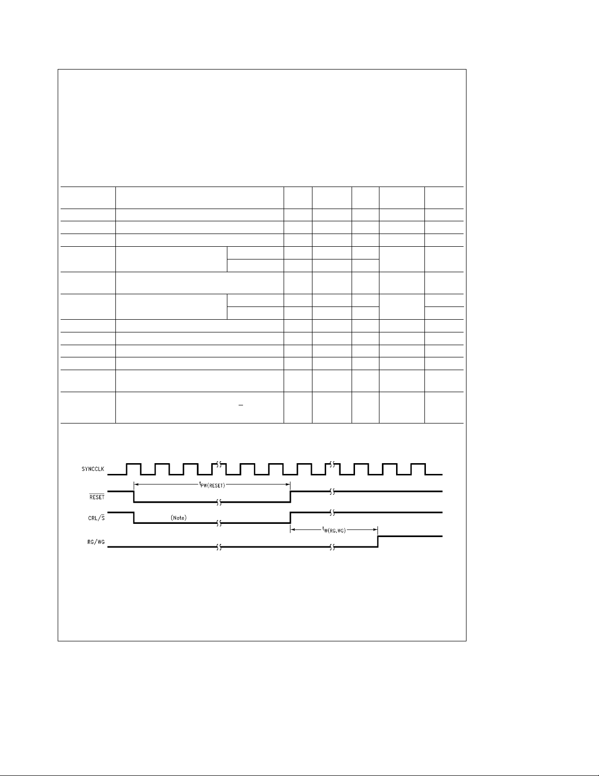
Note: Power down mode selected in control register (see Table I).
FIGURE 3. Reset Pin and Power Down Timing Diagram
TL/F/11963– 3
4
Page 5
Control Register Operating Conditions are guaranteed over operating conditions (see table) unless
otherwise specified.
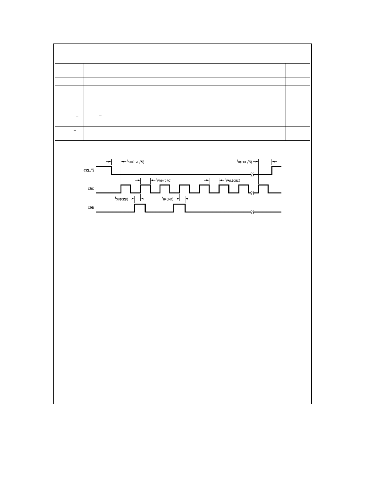
Symbol Parameter Min
t
PW(CRC)
t
SU(CRD)
t
H(CRD)
t
SU(CRL/S)
t
H(CRL/S)
Note 1: Typical values are specified at 25§C and 5V supply.
Note A: This parameter is guaranteed by outgoing testing.
CRC Pulse Width (positive or negative) (see
Figures 4
CRD Setup Time with respect to CRC (positive edge)
(see
Figures 4
and8)
CRD Hold Time with respect to CRC (positive edge)
(see
Figures 4
and8)
CRL/S Setup Time with respect to CRC (positive edge)
(see
Figures 4
and8)
CRL/S Hold Time with respect to CRC (positive edge)
(see
Figures 4
and8)
and9) 14 ns (Note A)
Typ
(Note 1)
Max Units Test
5 ns (Note A)
5 ns (Note A)
5 ns (Note A)
5 ns (Note A)
FIGURE 4. Control Register Timing Diagram
TL/F/11963– 4
5
Page 6

DC Electrical Characteristics are guaranteed over operating conditions (see table) unless otherwise speci-
fied.
Symbol Parameter Conditions Min
V
V
I
IN
I
OZ
I
DD
High Logic Level (Note 2) ECL
OH
Output Voltage Outputs
V
DD
I
OH
V
DD
I
OH
Low Logic Level (Note 2) ECL
OL
Output Voltage Outputs
V
DD
I
OL
V
DD
I
OL
Input Current V
TRI-STATE Output Current V
Supply TTL Code V
Current Output f
ECL Code Output
DD
DD
DD
NRZ
ECLV
e
e
e
e
e
e
e
e
e
e
e
e
CC
Min
20 mA
Min,
Max
Min,
20 mA
Min,
Max
ECLV
ECLV
Max,
50 Mb/s,
e
Max
Outputs
Outputs
CC
CC
e
e
TTL
TTL
Max
Max
0.815 ECLV
V
DD
3.5 (Note A)
0.575 ECLV
b
b
(Write Mode)
ECL Code Output
(Non-Write Mode)
I
DD(PD)
Supply Current in V
Power Down Mode
Note 1: Typical values are specified at 25§C and 5V supply.
Note 2: Assumes output is driving a 50 k X load.
Note A: This parameter is guaranteed by outgoing testing.
DD
e
ECLV
CC
e
Max
b
0.1 (Note A)
20 20 mA (Note A)
20 20 mA (Note A)
Typ
(Note 1)
CC
CC
Max Units Test
0.878 ECLV
0.705 ECLV
CC
CC
0.1 (Note A)
0.4 (Note A)
30 50
70 95 (Note A)
30 50 (Note A)
1 1.5 mA (Note A)
V
V
mA
(Note A)
(Note A)
(Note A)
6
Page 7

AC Electrical CharacteristicsÐWrite Mode are guaranteed over operating conditions (see table)
unless otherwise specified.
Symbol Parameter Conditions Min
t
SU(NRZIO(0,1))
t
H(NRZIO(0,1))
t
PD1
t
PD2
t
PD3
t
PD4
t
SU(EARLY)
t
H(EARLY)
t
SU(LATE)
t
H(LATE)
t
PW(WCLK)
Note 1: Typical values are specified at 25§C and 5V supply.
Note 2: A WCLK period is twice the NRZ rate period since a 2-bit interface is used.
Note 3: This specification is valid for either internal or external WCLK mode of operation.
Note A: This parameter is guaranteed by outgoing testing.
Note B: This specification is provided for information only.
NRZIO(0,1) Setup Time w.r.t. WCLK
(positive edge) (see
Figures 5
and8) (Note 3)
NRZIO(0,1) Hold Time w.r.t. WCLK
(positive edge) (see
Figures 5
and8) (Note 3)
Propagation Delay of Encoder, Precomp.
WCLK (positive edge) to CODEOUT Enabled 5
(positive edge) (Note 2) (see
Figures 5
and7)
Propagation Delay of Encoder, Precomp.
WCLK (positive edge) to CODEOUT Disabled 4
(positive edge) (Note 2) (see
Figures 5
and7)
Propagation Delay of Encoder, WG Precomp.
(positive edge) to First Valid CODE- Enabled 19
OUT Output (see
Figures 5
and7)
Propagation Delay of Encoder, WG Precomp.
(positive edge) to First Valid CODE- Disabled 14
OUT Output (see
Figures 5
and7)
EARLY Setup Time w.r.t. CODEOUT (positive edge) or CODEOUT 6 ns (Note A)
(negative edge) (see
Figures 5
and8)
EARLY Hold Time w.r.t. CODEOUT
(positive edge) or CODEOUT
edge) (see
Figures 5
(negative 6 ns (Note A)
and8)
LATE Setup Time w.r.t. CODEOUT
(positive edge) or CODEOUT
edge) (see
Figures 5
(negative 6 ns (Note A)
and8)
LATE Hold Time w.r.t. CODEOUT
(positive edge) or CODEOUT
tive edge) (see
Figures 5
(nega- 6 ns (Note A)
and8)
WCLK Pulse Width (High or Low)
(see
Figures 5
and9)
Typ
(Note 1)
Max Units Test
8 ns (Note A)
5 ns (Note A)
WCLK
PERIODS
WCLK
PERIODS
SYNCCLK
PERIODS
SYNCCLK
PERIODS
10 ns (Note A)
(Note B)
(Note B)
(Note B)
(Note B)
7
Page 8

AC Electrical CharacteristicsÐWrite Mode
FIGURE 5. Write Timing Diagram
TL/F/11963– 5
8
Page 9

AC Electrical CharacteristicsÐRead Mode are guaranteed over operating conditions (see table)
unless otherwise specified.
Symbol Parameter Min
t
SU(SYNCDAT)
t
H(SYNCDAT)
t
SU(NRZIO(0,1))
t
H(NRZIO(0,1))
t
PD5
t
PW(RRCLK)
Note 1: Typical values are specified at 25§C and 5V supply.
Note 2: A RRCLK period is twice the NRZ rate period since a 2-bit interface is used.
Note A: This parameter is guaranteed by outgoing testing.
Note B: The limit values have been determined by characterization data. No outgoing tests are performed.
SYNCDATA Setup Time w.r.t. SYNCCLK
(negative edge) (see
Figures 6
and8)
SYNCDATA Hold Time w.r.t. SYNCCLK
(negative edge) (see
Figures 6
and8)
NRZIO(0,1) Setup Time w.r.t. RRCLK
(positive edge) (see
Figures 6
and8)
NRZIO(0,1) Hold Time w.r.t. RRCLK
(positive edge) (see
Figures 6
and8)
Propagation Delay of Decoder, SYNCCLK
(negative edge) to RRCLK (Note 2) (see
RRCLK Pulse Width (High or Low) (see
Figures 6
Figures 6
and7) PERIODS
and9) 13 20 ns (Note A)
Typ
(Note 1)
Max Units Test
4 1 ns (Note A)
1 0 ns (Note A)
9 19 ns (Note A)
9 17 ns (Note A)
2
RRCLK
(Note B)
FIGURE 6. Read Timing Diagram
9
TL/F/11963– 6
Page 10

AC Electrical CharacteristicsÐGeneral are guaranteed over operating conditions (see table) unless
otherwise specified.
Symbol Parameter Min
t
ECLON
t
ECLOFF
t
WRTON
t
WRTOFF
Note 1: Typical values are specified at 25§C and 5V supply.
Note 2: The start and stop measurement voltage points are 1.3V.
Note 3: The start measurement voltage point is 1.3V and the stop measurement voltage point is V
Note A: This parameter is guaranteed by outgoing testing.
Note B: The limit values have been determined by characterization data. No outgoing test are performed.
ECL Section Turn On Time w.r.t. CRL/S pins
(positive edge) (see
Figures 6.5
and7) (Note 2)
ECL Section Turn Off Time w.r.t. CRL/S pins
(positive edge) (see
Figures 6.5
and10) (Note 3)
ECL Output Enabling Time w.r.t. WG Positive Edge
(see
Figure 6.5
)
ECL Output Disabling Time w.r.t. WG
negative edge (see
Figure 6.5
)
Typ
(Note 1)
Max Units Test
25ms (Note B)
24ms (Note B)
15 50 ns (Note A)
20 50 ns (Note A)
a
0.3V.
OL
Note 1: For t
Note 2: For t
, the ECL output mode is selected in the control register (see Table I).
ECLON
, the power down mode is selected in the control register (see Table I).
ECLOFF
FIGURE 6.5. ECL Code Write Timing Diagram
TL/F/11963– 7
10
Page 11

AC Electrical CharacteristicsÐWaveforms
FIGURE 7. Propagation Delay Waveforms
TL/F/11963– 11
TL/F/11963– 13
FIGURE 9. Input or Output Pulse Width Waveforms
FIGURE 8. Setup and Hold Time Waveforms
TL/F/11963– 12
TL/F/11963– 14
FIGURE 10. TRI-STATE Output Enable and Disable
Waveforms
11
Page 12

Functional Description
The Encoder/Decoder (ENDEC) translates NRZ data to and
from the (1,7) RLL format; receives and transfers NRZ data
in a 2-bit format; generates code output that can be made
either TTL or ECL compatible; indicates the need to precompensate write data and issues READ/REFERENCE
CLOCK (RRCLK). READ/REFERENCE CLOCK multiplexing is done without glitches.
Control Register
The control register is comprised of a fourteen-bit serial shift
register and a fourteen-bit latch
strobed into the shift register via the CONTROL REGISTER
DATA (CRD) input on the positive edge of the CONTROL
REGISTER CLOCK (CRC) input with the CONTROL REGISTER LATCH/SHIFT BAR (CRL/S
The information is parallel transmitted to the latch bank and
the ENDEC when the CRL/S
state. The control register truth table (Table I) describes the
functions controlled by each bit in the control register. The
bit at the right of each bit stream (13) in the table is the first
bit entered into the shift register.
Two bits of the control register (bits 1,2) control the power
down option. The other bits of the control register determine
various aspects of the ENDEC’s outputs. Bit4 inverts the
LSB MSB
012345678910111213
0xxxxxxxxx x x x x Reserved Bit
x00xxxxxxx x x x x Normal Operation
x11xxxxxxx x x x x Power Down
x x x 0 x x x x x x x x x x Reserved Bit
x x x x 1 x x x x x x x x x Inverts CODEOUT Data
xxxxx0xxxx x x x x Reserved Bit
xxxxxx1xxx x x x x Differential CODEOUT Data
xxxxxxx00x x x x x NoBypass
xxxxxxx01x x x x x Bypass Precompensation Circuit
xxxxxxx11x x x x x TRI-STATE CODEOUT Pin
xxxxxxxxx1 x x x x UseInternal Write Clock
xxxxxxxxxx 1 x x x Normal Operation
xxxxxxx00x x 1 x x Bypass Encoder
xxxxxxxxxx x x 0 x Reserved Bit
xxxxxxxxxx x x x 0 Reserved Bit
(Figure 11).
) pin at a logical low state.
input is taken to a logical high
Information is
TABLE I. Control Register Truth Table
BIT STREAM
sense of the CODEOUT output data. Bit 6 changes CODEOUT from a TTL compatible output to a ECL (differential)
compatible output. Bits 7, 8 controls bypass selection. No
bypass can be selected (bit7
sation circuit can be bypassed (bit7
CODEOUT pin can be tri-stated (bit7
permits the use of an internal write clock. Bit 10 must be set
to 1 for normal operation. Bit 11 puts the encoder in a bypass mode if bit 7 and bit 8 are also set to 0. In this mode,
the data received at the NRZIO0 pin will pass through the
encoder to the CODEOUT pin. All of the reserved bits (0, 3,
5, 12, 13) are to be programmed at a logical low level.
FIGURE 11. CTRL Register Block Diagram
e
bit8e0), the precompen-
e
0, bit8e1) and the
e
bit8e1). Bit 9
TL/F/11963– 8
Function Selected
12
Page 13

Functional Description (Continued)
1,7 RLL CODE
Ý
The (1,7) code used is based on US patent
cross-licensing with International Business Machines Corporation (IBM
used for this device. Nine SYNCDATA bits are used to decode the middle three SYNCDATA bits of the nine bit
stream into two NRZ output bits, a Most Significant Bit
(MSB) and a Least Significant Bit (LSB). Bit 8 is the first
SYNCDATA bit shifted into the decoder. The left-most column of the table (‘‘NRZIO OUTPUT BIT’’) identifies whether
the row represents the NRZ MSB or LSB. This table identifies the combinations which will produce a high logical level.
If the code bits do not match the table, a low logical state
will be produced. Table III represents the same decoding
operation in a different format.
Table IV summarizes the state diagram used by this device
to encode NRZ data into 1,7 coded data. The table is read
from left to right during the encoding process. To encode
data the ‘‘CURRENT STATE’’ (column 1) must be determined first.
). Table II summarizes the decoding method
É
Encoded Read Data (SYNCDATA) Decoded Data
Previous Present Next
Y1 Y2 Y3 Y1 Y2 Y3 Y1 Y2 Y3 D1 D2
MSBxLSB MSBxLSB MSBxLSB MSBxLSB
4,413,251 via
TABLE III. Decoding State Table
0000 1 1
1000000 1 1
1000001 0 1
1000010 0 1
1000100 0 1
1000101 0 1
The initial ‘‘CURRENT STATE’’ is always zero. This ‘‘CURRENT STATE’’ selects a group of four rows in the table. The
two NRZ input bits determine the exact row, within the
group, to be used. Once the row is identified, follow the row
to the right of the ‘‘NRZIO’’ column to locate the coded
output, in the ‘‘1,7 OUT’’ column. Continue by identifying the
next state in the ‘‘NEXT STATE’’ column immediately to the
right of the ‘‘1,7 OUT’’ column. The number located in this
column is used as the ‘‘CURRENT STATE’’ for the next two
NRZ input bits. This procedure is continued until all the NRZ
data is encoded.
TABLE II. Decoding State Table
NRZ OUTPUT SYNCDATA (CODE BITS)
BIT
NRZIO0 (LSB)e1 xxx1xxxxx
NRZIO1 (MSB)e1xxxxx1xxx
876543210
xxxx00xxx
xx000xxxx
xxxxxx000
(NRZ Data)
001 1 0
010000 1 0
010001 0 0
010010 0 0
010100 0 0
010101 0 0
100000 1 1
100001 0 1
100010 0 1
100100 0 1
100101 0 1
101 1 1
13
Page 14

Functional Description (Continued)
TABLE IV. Encoding State Table
NRZIO CODEOUT
CURRENT
STATE
0000100
0010102
0100104
0110103
1000000
1010002
1100004
1110003
2001000
2011002
2101004
2111003
3001010
3011011
3101014
3111001
4000010
4010011
4100014
4110101
Precompensation Outputs
The precompensation circuit in this ENDEC generates output data to be used externally to provide write precompensation. The precompensation truth table (Table V) demonstrates what outputs are expected per data sequence (bit
stream). In the table, the bit which is being considered for
ML
SS
BB
1,7 OUT
NEXT
STATE
precompensation is the target bit, T. This target bit is a logical high level. The location of data bits on either side of the
target bit indicates the logic states of the precompensation
outputs. No shift indicates that all the precompensation outputs are at a logical low level. The mention of a precompensation output in the ‘‘FUNCTION’’ column indicates that it is
at a logical high while those not mentioned are at a logical
low level.
TABLE V. Precompensation Truth Table
BIT STREAM
MSB LSB
0 0 T 0 0 NO SHIFT
1 0 T 0 1 NO SHIFT
1 0 T 0 0 EARLY
0 0 T 0 1 LATE
The EARLY and LATE outputs need to be connected to
inputs of a precompensation circuit to achieve write precompensation. Using the NSC DP8492 device as an example, the EARLY and LATE outputs of the ENDEC will be
connected to the EARLY and LATE inputs to the DP8492,
respectively.
Address Mark Mode
Hard Sectored Read Mode
This ENDEC supports only a 3T preamble pattern. At the
assertion of READ GATE, the decoder searches for 16 uninterrupted code pulses of (3T) preamble. Once the preamble counter has filled to a count of 16, an internal preamble
detected signal is issued. It resets an internal state machine
and initiates the phase synchronization process. Decoding
of 1,7 data will begin after phase synchronization.
Hard Sectored Write Mode
At the assertion of WRITE GATE with NRZIO inputs held
low, the encoder issues (3T) preamble at the CODEOUT
pin. Preamble will continue until the first non-zero NRZ input
bit appears.
(Figure 13)
(Figure 12)
FUNCTION
FIGURE 12. Hard Sectored Write Mode Waveforms
FIGURE 13. Hard Sectored Read Mode Waveforms
14
TL/F/11963– 9
TL/F/11963– 10
Page 15

Physical Dimensions inches (millimeters)
20-Pin Small Outline Package
Order Number DP84902M
NS Package Number M20B
15
Page 16

Physical Dimensions inches (millimeters) (Continued)
DP84902 1,7 Encoder/Decoder Circuit
20-Pin Shrink Small Outline Package
Order Number DP84902MS
NS Package Number MSA20
LIFE SUPPORT POLICY
NATIONAL’S PRODUCTS ARE NOT AUTHORIZED FOR USE AS CRITICAL COMPONENTS IN LIFE SUPPORT
DEVICES OR SYSTEMS WITHOUT THE EXPRESS WRITTEN APPROVAL OF THE PRESIDENT OF NATIONAL
SEMICONDUCTOR CORPORATION. As used herein:
1. Life support devices or systems are devices or 2. A critical component is any component of a life
systems which, (a) are intended for surgical implant support device or system whose failure to perform can
into the body, or (b) support or sustain life, and whose be reasonably expected to cause the failure of the life
failure to perform, when properly used in accordance support device or system, or to affect its safety or
with instructions for use provided in the labeling, can effectiveness.
be reasonably expected to result in a significant injury
to the user.
National Semiconductor National Semiconductor National Semiconductor National Semiconductor
Corporation Europe Hong Kong Ltd. Japan Ltd.
1111 West Bardin Road Fax: (
Arlington, TX 76017 Email: cnjwge@tevm2.nsc.com Ocean Centre, 5 Canton Rd. Fax: 81-043-299-2408
Tel: 1(800) 272-9959 Deutsch Tel: (
Fax: 1(800) 737-7018 English Tel: (
National does not assume any responsibility for use of any circuitry described, no circuit patent licenses are implied and National reserves the right at any time without notice to change said circuitry and specifications.
Fran3ais Tel: (
Italiano Tel: (
a
49) 0-180-530 85 86 13th Floor, Straight Block, Tel: 81-043-299-2309
a
49) 0-180-530 85 85 Tsimshatsui, Kowloon
a
49) 0-180-532 78 32 Hong Kong
a
49) 0-180-532 93 58 Tel: (852) 2737-1600
a
49) 0-180-534 16 80 Fax: (852) 2736-9960
 Loading...