

Page 1
DP8459 All-Code Data Synchronizer
General Description
The DP8459 Data Synchronizer is an integrated phase
locked loop circuit which has been designed for application
in magnetic hard disk, flexible (floppy) disk, optical disk, and
tape drive memory systems for data re-synchronization and
clock recovery with any standard recording code, operating
to 25 Mb/s. The DP8459 is provided in a 28-pin PCC
package. Zero phase start is employed during both data and
reference clock lock sequences for rapid acquisition. An
optional (Customer-controlled) synchronization field
frequency-acquisition feature guarantees lock, accommodating the preamble types used with GCR (Group Code
Recording), MFM (Modified Frequency Modulation), the
[1,N] run length limited (RLL) codes, and either of the
standard 2,7 RLL codes. Precise synchronization window
generation is achieved via an internal, self-aligning delay line
which remains accurate independent of temperature, power
supply, external component and IC process variations. The
DP8459 also incorporates a digitally controlled ( MICROW-
™
IRE
bus compatible) strobe function with 5-bit resolution
which allows for margin testing, error recovery routines, and
precise window calibration. The PLL filter resides external to
the chip, with two ports provided to allow significant design
flexibility.Synchronizationpattern detection circuitry issues a
PREAMBLE DETECTED signal when a pre-determined
length of the user-selected pattern is encountered. All digital
input and output signals are TTL compatible and a single,
+5V power supply is required. The DP8459V is offered as a
DP8459V-10 (250 Kbit/sec thru 10 Mbits/sec) or
DP8459V-25 (250 Kbits/sec thru 25 Mbit/sec), see AC
Electrical Characteristics.
Features
n Fully integrated dual-gain PLL
n Zero phase start lock sequence
n 250 Kbit/sec–25 Mbit/sec data rate range
n Frequency lock capability (optional) for all standard
recording codes
n Digital window strobe control, 5-bit resolution
n Two-port PLL filter network
n PLL free-run (Coast) control for optical disk defects
n Synchronization pattern (preamble lock) detection
n Non-glitching multiplexed read/write clock output
n +5V supply
n DP8459 supplied in 28-pin plastic chip carrier (PCC)
and 40-pin TapePak packages
ADVANCED
December 1995
DP8459 All-Code Data Synchronizer
DP8459
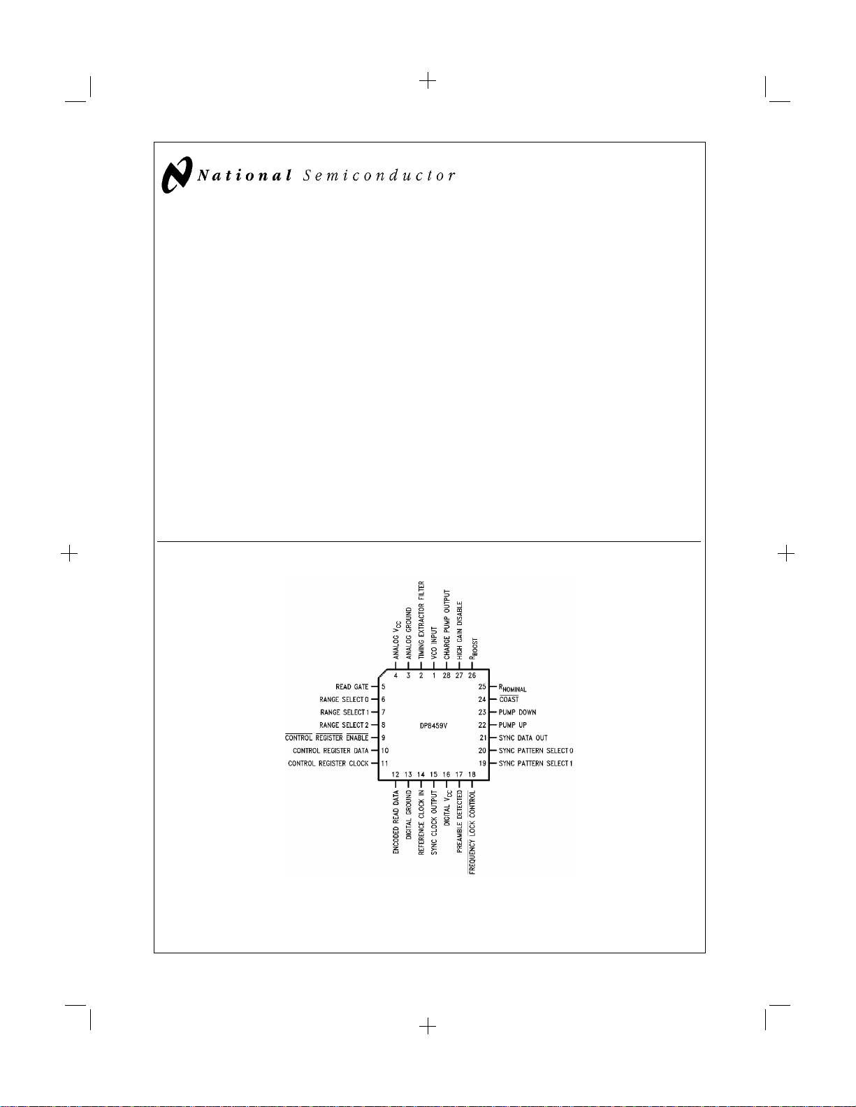
Connection Diagrams
TL/F/9322-6
FIGURE 1. DP8459 in 28-Pin Plastic Chip Carrier (PCC) V-Type Package Order Number DP8459V-10 or DP8459V-25
TapePak®is a registered trademark of National Semiconductor Corporation.
™
MICROWIRE
is a trademark of National Semiconductor Corporation.
© 1996 National Semiconductor Corporation TL/F/9322 http:\\www.national.com 1
PrintDate=1996/07/31 PrintTime=11:05:38 ds009322 Rev. No. 1 Proof 1
Page 2
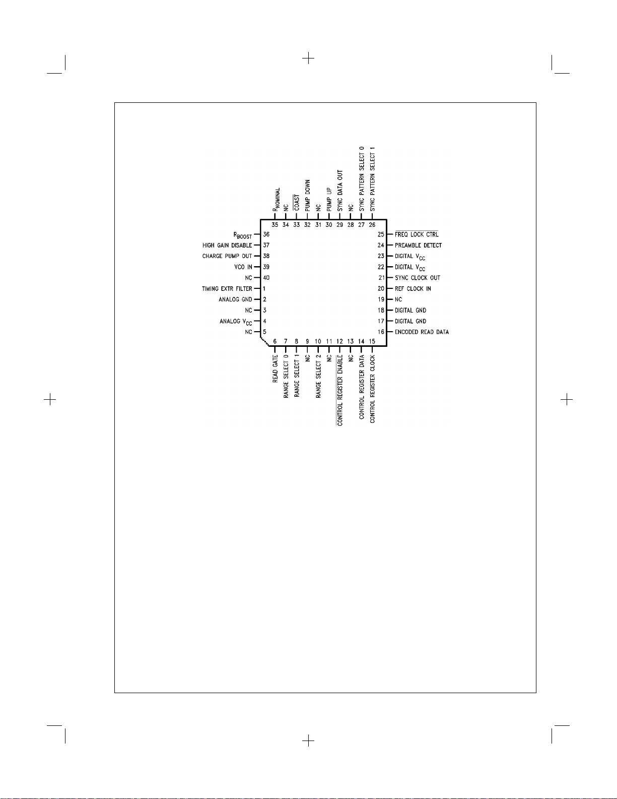
Connection Diagrams
TapePak
®
Top ViewOrder Number DP8459TP-10 or DP8459TP-25See NS Package TP40A
2 http:\\www.national.com
TL/F/9322-39
PrintDate=1996/07/31 PrintTime=11:05:39 ds009322 Rev. No. 1 Proof 2
Page 3
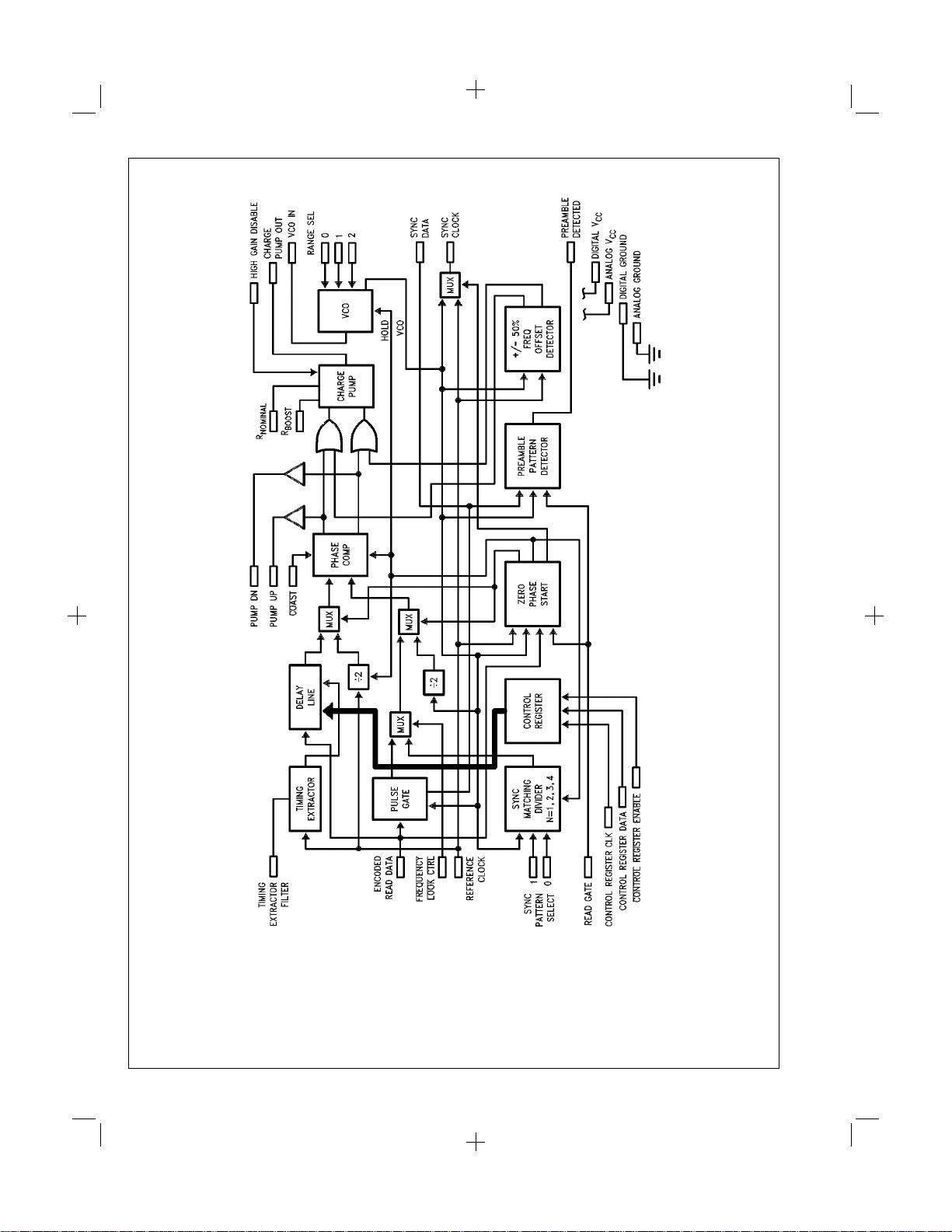
System Diagram
TL/F/9322-8
FIGURE 2. DP8459 System Block Diagram
http:\\www.national.com 3
PrintDate=1996/07/31 PrintTime=11:05:39 ds009322 Rev. No. 1 Proof 3
Page 4
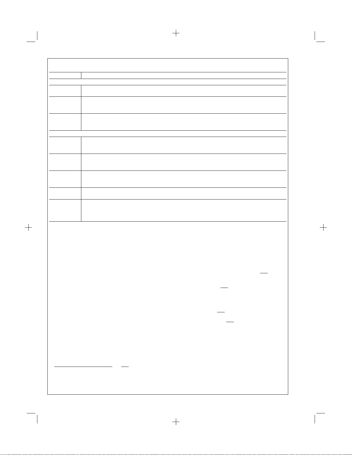
1.0 Pin Descriptions
DP8459 28-pin PCC package
#
Pin
POWER SUPPLY
16 DIGITAL V
4 ANALOG V
13 DIGITAL GROUND.
3 ANALOG GROUND.
TTL LEVEL LOGIC INPUTS
5 READ GATE (RG): Read mode control input, active high (logical-one). Assertion causes the PLL to lock to
the ENCODED READ DATA, employing a zero phase start routine. Deassertion causes the PLL to lock the
REFERENCE CLOCK input, also employing a zero phase start routine. READ GATE timing is allowed to
be fully asynchronous.
6, 7, 8 RANGE SELECT 0, 1, 2 (RS0, RS1, RS2): Control the operating frequency range of the VCO. A 2:1
continuously variable sub-range is available within each of 6 allowed selections, enabling the VCO to
operate at any frequency within a 96:1 range from 500 kHz to 50 MHz.
9 CONTROL REGISTER ENABLE (CRE): A logical Low level allows the CONTROL REGISTER CLOCK to
clock data into the Control Register via the CONTROL REGISTER DATA input; a logical HIGH level
latches the register data and issues the information to the appropriate circuitry.
10 CONTROL REGISTER DATA (CRD): Control Register data input.
11 CONTROL REGISTER CLOCK (CRC): Negative edge triggered Control Register clock input.
12 ENCODED READ DATA (ERD): Incoming TTL-level data derived from the storage media; issued from a
pulse detector circuit. Each positive edge represents a single recorded code bit.
14 REFERENCE CLOCK (RFC): A reference frequency input required for DP8459 operation. The RFC
frequency must be accurate and highly stable (crystal or servo derived) and equivalent to the 2F frequency
for the MFM or [2,7] codes (i.e., equal to, but not derived from the VCO frequency).
18 FREQUENCY LOCK CONTROL (FLC): Selects or de-selects the frequency lock function during a READ
operation. Has no effect with READ GATE deasserted; frequency lock is automatically employed for the full
duration of time READ GATE is deasserted regardless of the level of the FLC input. With READ GATE
high and FLC low (logical-zero) the PLL is forced to lock to the pattern frequency selected via the SYNC
PATTERN SELECT inputs. When high (logical-one) frequency lock action is terminated and the PLL
employs a pulse gate to accommodate random disk data patterns. FLC may be tied to PREAMBLE
DETECTED output pin for self-regulated frequency lock control. FLC timing is allowed to be fully
asynchronous.
20, 19 SYNC PATTERN SELECT 0, 1 (SP0, SP1): Control inputs for selection of the preamble type being
employed. These inputs determine the pattern to which the PLL will frequency-lock during preamble
acquisition (if frequency lock is employed) and for which the PREAMBLE DETECTED circuitry searches.
24 COAST (CST): Control for Coast function. The Coast function may be activated when READ GATE is
either high or low. When the COAST input is low (logical-zero), the phase comparator is disabled and held
in a cleared state, allowing the VCO to coast regardless of ENCODED READ DATA input activity (READ
GATE high) or REFERENCE CLOCK input activity (READ GATE low). No other circuit functions are
disturbed. When high (logical-one), the phase comparator operates normally.
27 HIGH-GAIN DISABLE (HGD): Charge Pump gain switch control. When low (logical-zero), the charge pump
input current is the combined value of the currents at both R
(logical-one), charge pump input current is taken from the R
READ GATE or PREAMBLE DETECTED for self-regulated gain control.
TTL LEVEL LOGIC OUTPUTS
15 SYNCHRONIZED CLOCK (SCK): Issues the VCO signal following READ GATE assertion and completion
of zero phase start sequence; issues REFERENCE CLOCK input signal when READ GATE is deasserted.
Multiplexer switching is achieved without glitches.
17 PREAMBLE DETECTED (PDT): Issues a high level (logical-one) following assertion of READ GATE,
completion of the zero phase start sequence, and the detection of approximately 32 sequential pulses of
1T, 2T or 3T period preamble, or 16 sequential pulses of 4T period preamble, depending on state of SYNC
PATTERN SELECT inputs (T=VCO period). Following preamble detection, the output remains latched
high until de-assertion of READ GATE. The PDT output will be at a logical zero state whenever READ
GATE is inactive.
: 5.0V±5%. (Note 1 )
CC
: 5.0V±5%. (Note 1 )
CC
and R
BOOST
pin only. HGD may be tied either to
NOMINAL
NOMINAL
pins. When high
4 http:\\www.national.com
PrintDate=1996/07/31 PrintTime=11:05:40 ds009322 Rev. No. 1 Proof 4
Page 5
1.0 Pin Descriptions (Continued)
#
Pin
TTL LEVEL LOGIC OUTPUTS
21 SYNCHRONIZED DATA (SD): A reconstructed replica of the ENCODED READ DATA signal,
22 PUMP UP (PU): Active HIGH whenever the phase comparator issues a pump-up signal to the charge
23 PUMP DOWN (PD): Active HIGH whenever the phase comparator issues a pump-down signal to the
ANALOG SIGNAL PINS
28 CHARGE PUMP OUTPUT: The output of the high-speed, switching bi-directional current source circuitry of
1 VCO INPUT: The high-impedance control voltage input to the voltage controlled oscillator (VCO). The
2 TIMING EXTRACTOR FILTER: A pin for the connection of external, passive components employed to
25 R
26 R
Note 1: These pins should always be tied together; they are not intended to be used with separate power supplies.
time-stabilized and synchronized to the SYNCHRONIZED CLOCK output.
pump. The PU pin is an open-emitter output requiring an external passive pull down resistor whenever in
active use. The output should be allowed to float when not needed.
charge pump. The PD pin is an open-emitter output requiring an external passive pull down resistor
whenever in active use. The output should be allowed to float when not needed.
the charge pump. The external, passive PLL filter network is established between this pin, the VCO INPUT
pin, and ground.
external, passive PLL filter network is established between this pin, the CHARGE PUMP OUTPUT pin, and
ground.
stabilize the delay line timing extraction circuitry. Delay accuracy is not a function of external component
values or tolerances.
: A resistor is tied between this pin and VCCto set the charge pump
NOMINAL
The current is internally multiplied by 2 for charge pump use.
: A resistor is tied between this pin and VCCto set the charge pump
BOOST
resistor is effectively paralleled with the R
R
BOOST
inactive (logical-zero); thus the sum of the resistor currents sets the total input current. The input current is
resistor when the HIGH GAIN DISABLE input is
NOMINAL
nominal
operating current.
boost
(or adder) current. The
multiplied by 2 within the charge pump circuitry.
2.0 Circuit Operation
In the non-Read mode, the DP8459 PLL is locked to the
REFERENCE CLOCK signal. This permits the VCO to remain
at a frequency very close to the encoded data clock rate while
the PLL is “idling” and thus will minimize the frequency step
and associated lock time encountered at the initiation of lock to
ENCODED READ DATA. Frequency acquisition is employed
in the non-Read mode to ensure lock.
Note: The REFERENCE CLOCK signal is employed bycircuitrywhich sets the
time delay of the internal delay line. This requires the REFERENCE CLOCK
signal to be present
DP8459 operation.
at all times
at a stable and accurate frequency for proper
At the assertion of READ GATE, which is allowed to be done
asynchronously (no timing requirements), and following the
completion of two subsequent VCO cycles, the DP8459 VCO
is stopped momentarily and restarted in accurate phase
alignment with the second data bit which arrives following the
VCO pause. This minimization of phase misalignment
between the ENCODED READ DATAand the VCO (referred to
as zero phase start, or ZPS) significantly reduces data lock
acquisition time.
The DP8459 incorporates a preamble-specific frequency
acquisition feature which may be employed at the user’s
option. The frequency acquisition feature is intended
specifically for use within hard or pseudo-hard sectored
systems where READ GATE is asserted only within a
preamble. With the READ GATE active (logical-one) and the
FREQUENCY LOCK CONTROL (FLC) input active
(logical-zero), the DP8459 will be forced to lock to the exact
preamble frequency selected at the SYNC PATTERN SELECT
inputs. The frequency discriminating action of the PLL
http:\\www.national.com 5
provided in this mode produces a lock-in range equivalent to
the available VCO operating range and thus eliminates the
possibility of fractional-harmonic lock. Windowing (pulse gate
action; see Pulse Gate, Section 2.1) is not employed in the
frequency acquisition mode and thus quadrature lock is
prevented (see National Semiconductor Application Note
AN-414, APPS Mass Storage Handbook
#
1, 1986, for an
explanation of typical false lock modes). The DP8459 will
remain in the frequency acquisition mode until the FLC input is
deactivated (logical-one). In ordinary hard sectored or
pseudo-hard sectored operation, the PREAMBLE DETECTED
(PDT) output is tied to the FLC input for automatic switching
from frequency acquisition to phase lock following internal
detection of the selected preamble by the DP8459. The
Customer may choose to intervene in this path and extend the
frequency lock period. However, the DP8459
must
be placed
in the phase lock mode (FLC deactivated—logical-one) prior
to encountering the end of the preamble, or loss of lock will
result. Switching of the FLC input may be done
asynchronously (no set-up or hold timing requirements).
The PREAMBLE DETECTED (PDT) output will become active
(logical-one) following READ GATE assertion, completion of
the ZPS sequence and the subsequent detection of
approximately 32 ENCODED READ DATA(ERD) pulses of the
1T, 2T or 3T preamble types, or 16 ENCODED READ DATA
(ERD) pulses of the 4T preamble type (see specification
tables), and will remain active (logical-one) until deassertion of
READ GATE.
The Customer has the option of employing an elevated PLL
bandwidth during preamble acquisition (or at any other time)
for an extended capture range. An R
pin is provided to
BOOST
PrintDate=1996/07/31 PrintTime=11:05:41 ds009322 Rev. No. 1 Proof 5
Page 6
allow for an increase in charge pump gain above the level set
by the R
(HGD) is inactive (logical-zero), the R
electrically paralleled with the R
charge pump gain. When HIGH GAIN DISABLE is active
(logical-one), only the R
pump current. The Charge Pump throughput gain is I
I
where I
Rp
=
R
R
p
NOM
to configure the system for high gain prior to DP8459 preamble
pin. When the HIGH GAIN DISABLE pin
NOMINAL
NOMINAL
resistor is employed to set the
NOMINAL
=
0.25V
Rp
||R
CC/Rp,Rp
with HGD low.The Customer may choose
BOOST
=
R
NOM
resistor is
BOOST
for an elevated
=
2x
with HGD high, and
CPO
detection by tying the HGD pin to the PDT output pin, or for
high gain only during REFERENCE CLOCK lock by tying the
HGD pin to the READ GATE pin. Other configurations may be
employed, if desired.
The DP8459 issues a clock waveform from the SYNCHRONIZED CLOCK output which is derived from the REFERENCE
CLOCK input when the READ GATE is inactive (logical-zero),
and from the VCO signal following READ GATE assertion
(logical-one) and completion of the zero phase start sequence.
The REFERENCE CLOCK signal is issued from the
SYNCHRONIZED CLOCK output during non-Read activity
and may be used as a write clock, if desired. Once data lock is
achieved and the SYNCHRONIZED CLOCK output is issuing
VCO, the SYNCHRONIZED DATA output and the SYNCHRONIZED CLOCK output are held in a fixed, specified timing
relationship for use by decoding/deserializing circuitry. The
SYNCHRONIZED CLOCK output multiplexer switching is
achieved without glitches, i.e., no pulse is narrower than 50
of the VCO or REFERENCE CLOCK period.
The DP8459 provides a COAST control input which serves to
clear the phase comparator and disable charge pump action
whenever taken to an active, logical-zero level. This function is
made available to allow the PLL to be set to free-run,
undisturbed, while a detectable defect is being read from the
media in a region where re-initiation of the lock procedure is
impractical (e.g., data field). External data controller circuitry is
responsible for the detection of the defect and issuance of the
COAST command. The primary application of this feature is
expected to be optical disk bright-spot avoidance, though it will
lend itself to other applications as well.
As in the previous family of National Semiconductor data
separators/synchronizers, the DP8459 provides phase
comparator activity information to the Customer. The phase
comparator’s pump-up and pump-down outputs are brought
out to separate pins, PUMP UP (PU) and PUMP DOWN (PD).
The outputs are of the open-emitter type, requiring an external
“pull-down” resistor when in active use. These outputs serve to
indicate the relative displacement of the current data bit with
respect to the internal VCO phase (window center). When in
completely stabilized lock with no bit displacement, the
output(s) will issue a pulse of a finite, minimum-valued width
for each arriving data pulse. If any data pulse is displaced with
respect to the VCO phase, the corresponding output pulse will
widen by an amount equivalent to the bit displacement. These
output signals may be integrated over time and employed to
determine the average magnitude of media bit shift.
Additionally, the pulse widening/narrowing effect bit displacement has on the PU/PD outputs produces an amplitude
modulation of the output’s waveform. The waveform envelope,
when observed with a relatively slow oscilloscope time base,
can be employed for observation of PLL dynamics. This is
particularly useful if intrusive probing of the PLL filter nodes is
not desirable.
It is strongly recommended that the PU/PD outputs be left
“floating” (unconnected to any net or circuit element, including
the output pull-down resistor) in any application where they are
not specifically needed. This will serve to minimize
unnecessary, spurious digital switching transients in the
vicinity of the DP8459, and thus improve noise performance.
The DP8459 provides a wide operating data rate range to
facilitate use within a broad base of applications, including
multiple data rate systems or constant density recording
(CDR). In order to achieve the specified 250 kbit /sec to 25
Mbit/sec span, the operation of the VCO has been divided into
6 contiguous frequency sub-ranges, with approximately a 2:1
ratio between adjacent range selections. Three inputs are
provided for selecting of the sub-ranges, RANGE SELECT 0, 1
and 2. Some code type restrictions have been placed on the
higher ranges of operating VCO frequency. See
the operating data rate truth table and allowed code type
versus VCO range selection.
The DP8459 allows for flexible synchronization window strobe
%
control. The inputs CONTROL REGISTER DATA (CRD),
CONTROL REGISTER CLOCK (CRC), and CONTROL
REGISTER ENABLE (CRE) are configured to permit
interfacing of the DP8459 to the MICROWIRE™(or
equivalent) bus for entry of strobe information. Information is
serially shifted into the CONTROL REGISTER via the CRD
and CRC pins whenever the CRE pin is active (logical-zero).
When the CRE pin is inactive (logical-one), CRD and CRC are
ignored. The strobe function allows the Customer to shift the
synchronization window in 31 equal steps of magnitude t
x [1.8%x τ
respect to nominal window position. This function may be
] from approximately 27%early to 27%late with
VCO
employed for margin testing (eg., approximately
error recovery read re-try operations (eg., approximately
±
to
3%). Additionally, this feature allows the Customer to align
the center of the synchronization window to within one half
strobe step of ideal, regardless of the initial performance or
specification of the DP8459. This window centering function
may be performed completely within the drive system itself
(auto-alignment) given the employment of an intelligent
window alignment routine. Such a routine would be configured
to determine the maximum error free early and late window
positions via the strobe function, and then would fix the
DP8459 window in the arithmetic mean position (Section
4.3.3). See
Note: In all DP8459 applications, provision must be made to load the
appropriate information into the Control Register.
Figure 4
for a window strobe truth table.
Figure 3
±
12%)or
for
=
M
S
±
%
2
6 http:\\www.national.com
PrintDate=1996/07/31 PrintTime=11:05:43 ds009322 Rev. No. 1 Proof 6
Page 7
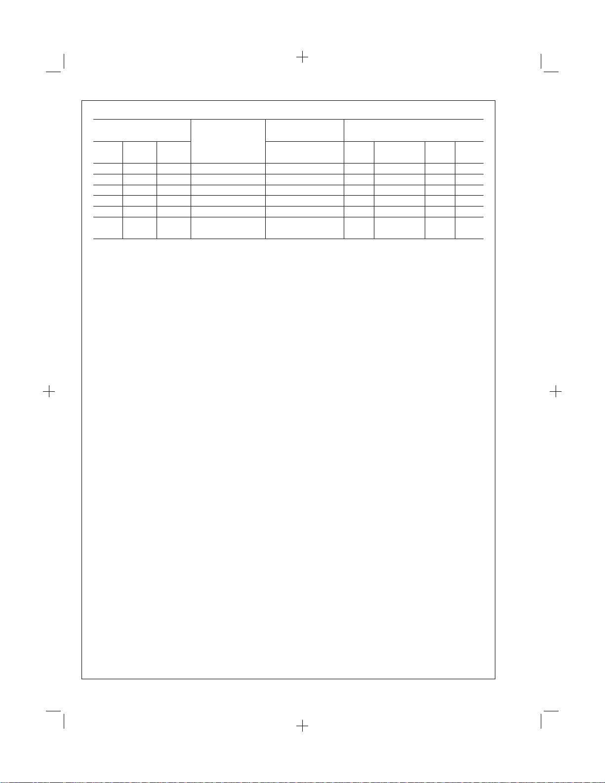
RANGE SELECT Input Equivalent Minimum N (Allowed Code Type)
( Note 1 ) VCO Range NRZ Data Rate
2 1 0 MHz MFM or 2,7 1 2 3 4
(Mbit/sec) (GCR) (MFM; 1, N) (2,7) (2,7)
1 1 X 0.50 ≤ Fvco ≤ 1.25 0.250≤ Fnrz ≤ 0.625
1 0 1 1.25<Fvco ≤ 2.5 0.625<Fnrz ≤ 1.25
1 0 0 2.5<Fvco ≤ 5 1.25<Fnrz ≤ 2.5
01 1 5
01 010
00X20
<
Fvco ≤ 10 2.5<Fnrz ≤ 5
<
Fvco ≤ 20 5<Fnrz ≤ 10 N/A
<
Fvco ≤ 50 10<Fnrz ≤ 25 N/A
√√√√
√√√√
√√√√
√√√√
√√√
√√√
(Note3)
Note 1: N/A—Not Allowed.
Note 2: Operation slightly beyond listed range boundaries may be acceptable in some applications.At or near range boundaries, range selection should be made
to place the operating frequency near the UPPER boundary; e.g., use RS2=0, RS1=1, and RS0=0 for 10 Mb/s.
Note 3: 20 MHz
<
Fvco ≤ 38 MHz for 1, N codes.
FIGURE 3. Code Type Allowance Versus VCO Frequency Range
http:\\www.national.com 7
PrintDate=1996/07/31 PrintTime=11:05:45 ds009322 Rev. No. 1 Proof 7
Page 8
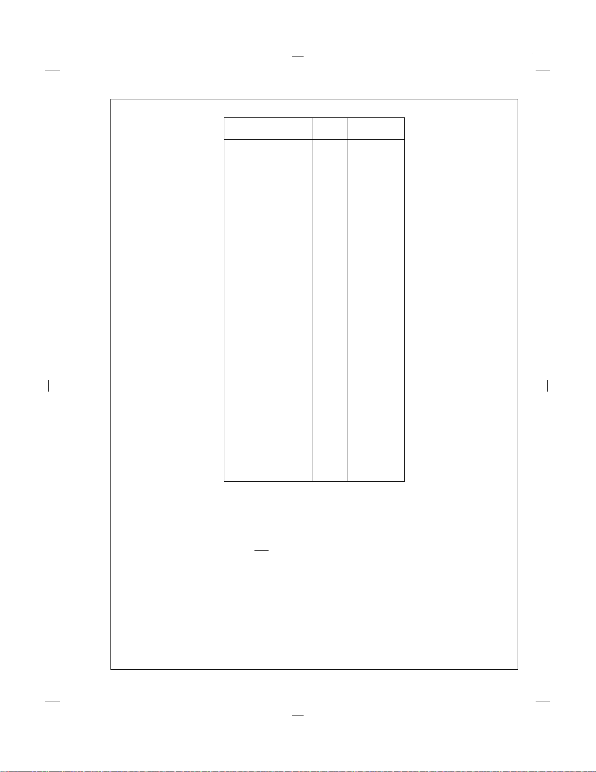
Strobe Bit Strobe Window Strobe
43210Word M T
01111 −15 −0.270 x τ
01110 −14 −0.252 x τ
01101 −13 −0.234 x τ
01100 −12 −0.216 x τ
01011 −11 −0.198 x τ
01010 −10 −0.180 x τ
01001 −9 −0.162 x τ
01000 −8 −0.144 x τ
00111 −7 −0.126 x τ
00110 −6 −0.108 x τ
00101 −5 −0.090 x τ
00100 −4 −0.072 x τ
00011 −3 −0.054 x τ
00010 −2 −0.036 x τ
00001 −1 −0.018 x τ
00000 0 0
10000 0 0
10001 1 0.018 x τ
10010 2 0.036 x τ
10011 3 0.054 x τ
10100 4 0.072 x τ
10101 5 0.090 x τ
10110 6 0.108 x τ
10111 7 0.126 x τ
11000 8 0.144 x τ
11001 9 0.162 x τ
11010 10 0.180 x τ
11011 11 0.198 x τ
11100 12 0.216 x τ
11101 13 0.234 x τ
11110 14 0.252 x τ
11111 15 0.270 x τ
FIGURE 4. Window Strobe Truth Table
Customers who employ the DP8459 in a system without a
MICROWIRE
™
(or functionally equivalent) bus configuration
and who wish to fix the synchronization window in the nominal
position while deselecting the test mode need only load
all-zero’s into the Control Register following power-up; this
may be easily achieved in some system configurations
(requiring no additional hardware) by tying CRE to RG, tying
CRC to ERD and tying CRD to ground, providing the
necessary waveforms are present for register loading prior to
the first read operation.
The DP8459 provides two pins for PLL filtering purposes,
CHARGE PUMP OUTPUT (CPO) and VCO INPUT (VCOI).
These provide the Customer with great flexibility in fliter
design, permitting high-order filter functions for optimization of
PLL lock characteristics and bit jitter rejection. For basic 3rd
order applications, CPO and VCOI may be tied together
(Typical)
S
VCO
VCO
VCO
VCO
VCO
VCO
VCO
VCO
VCO
VCO
VCO
VCO
VCO
VCO
VCO
VCO
VCO
VCO
VCO
VCO
VCO
VCO
VCO
VCO
VCO
VCO
VCO
VCO
VCO
VCO
(single-node) with a simple lead-lag, C||(R+C) filter tied
between these pins and ground. More esoteric filter designs
may be implemented if the pins are electrically separated and
a two-port filter network is established between CPO, VCOI,
and ground. National Semiconductor supplies initial PLL filter
recommendations for the single-node configuration within this
data sheet with the qualifying statement that they are very
general in nature, intended primarily for production testing of
static window margin, and are NOT optimized for any
particular disk system. For optimum performance, the
Customer should pursue a filter design which is individualized
and tailored to the requirements of the specific system
involved. This is particularly true for the two-port filtering
technique. See
Figure 5
for initial single-node filter design
recommendations.
8 http:\\www.national.com
PrintDate=1996/07/31 PrintTime=11:05:47 ds009322 Rev. No. 1 Proof 8
Page 9
Code MFM MFM MFM 2,7 2,7 Units
Rate 0.500 2 5 10 20 Mbit/sec
VCO freq. 1 4 10 20 40 MHz
Sync bytes 12 12 12 12 12 bytes
pulses/byte 8 8 8 4 4 flux tran’s
sync length 192 48 19.2 9.6 4.8 µs
sync freq 0.500 2 5 5 10 MHz
N
sync
N
max/Nmin
ζ
min
ζ
max
ζ
sync
ω
sync
C1 0.5 0.12 0.05 0.018 8200 pF µF
2 2 2 4 4 none
4/2 4/2 4/2 8/3 8/3 none
0.5 0.5 0.5 0.5 0.5 none
0.7 0.7 0.7 0.8 0.8 none
0.7 0.7 0.7 0.7 0.7 none
35 144 353 606 1230 Krad/sec
*
R1 82 82 82 150 150 Ω
C2 0.01 µF 2700 1000 510 200 pF
Note 1: Preamble (sync) natural frequency chosen yields phase error ≤ 0.01 radians at sync field end, given a 1%frequency step at READ GATE assertion. Rnom
=
Rboost=2.4k for all above loop filter selections. HGD is tied to RG, FLC is tied to PD and CPO is tied to VCOI as well as to the loop flter components.
Note 2: Component values are listed for purposes of window specification testing and correlation. These values do not necessarily yield optimum performance in
actual system applications. PLL dynamics and code characteristics are presented for Customer information and convenience only. See Section 3.1.
*
Unless otherwise noted.
FIGURE 5. Test Conditions and Component Values for Static Window Truncation Testing
The DP8459 VCO is constrained at all times to operate within
a frequency swing of approximately
±
50%of the frequency
present at the REFERENCE CLOCK input. Internal frequency
detector/comparator circuitry senses when the VCO overruns
the 50%boundary and forces the charge pump to move the
VCO back toward the REFERENCE CLOCK frequency until
the 50%constraint is again satisfied—thus preventing VCO
runaway in the event of loss of lock or during extended periods
where ENCODED READ DATAis not present.Additionally, this
technique causes the filter node voltage to behave as if a
voltage clamp were present at the Charge Pump Output,
preventing the control voltage, in the event of loss of lock, from
drifting outside of its operating range and inadvertently
extending lock recovery time.
A special test mode feature has been incorporated into the
DP8459 which allows a specific input pin to change function
and act as an excitation source (substitute VCO) for clocking
internal logic circuitry. When the last bit in the CONTROL
REGISTER is taken to a logical ONE, the VCO is stopped, and
the HGD input is redirected to act as a clock source for the
VCO divider circuitry. Additionally, the Delay Line and Timing
Extractor blocks are disabled when the Test Mode is entered,
and thus the device will not function normally and should not
2.1 Functional Block Description
PULSE GATE
The function of the Pulse Gate within the DP8459 is twofold.
First, the block contains the ECL flip-flop which captures each
arriving ENCODED READ DATAbit and transmits the bit to the
SYNCHRONIZED DATA output. The very high switching
speed of the bit-capture ECL flip-flop minimizes the portion of
window margin loss caused by flip-flop metastability at window
boundaries. Second, the Pulse Gate regulates the
transmission of the VCO waveform into the Phase
Comparator, allowing only one VCO pulse to pass with each
arriving ENCODED READ DATA pulse. See
Figure 6
for a
simplified logical representation of the Pulse Gate block. The
one-to-one data/VCO pulse ratio produced by the Pulse Gate
permits the multiple-harmonic nature of encoded data to be
accommodated by the phase/frequency comparator. During
the non-Read mode or during the portion of the Read mode
within which the Customer has set the FREQUENCY LOCK
CONTROL pin to a logical-zero (low), the Pulse Gate is
inactive (bypassed) and the VCO frequency is divided as
appropriate to match the incoming frequency source
(ENCODED READ DATAor the REFERENCE CLOCK input).
be operated in this mode for purposes other than internal gate
exercising. Further information regarding application of the
Test Mode will be furnished at the Customer’s request: contact
National Semiconductor Logic Marketing Group or Logic
Applications Group.
http:\\www.national.com 9
PrintDate=1996/07/31 PrintTime=11:05:48 ds009322 Rev. No. 1 Proof 9
Page 10
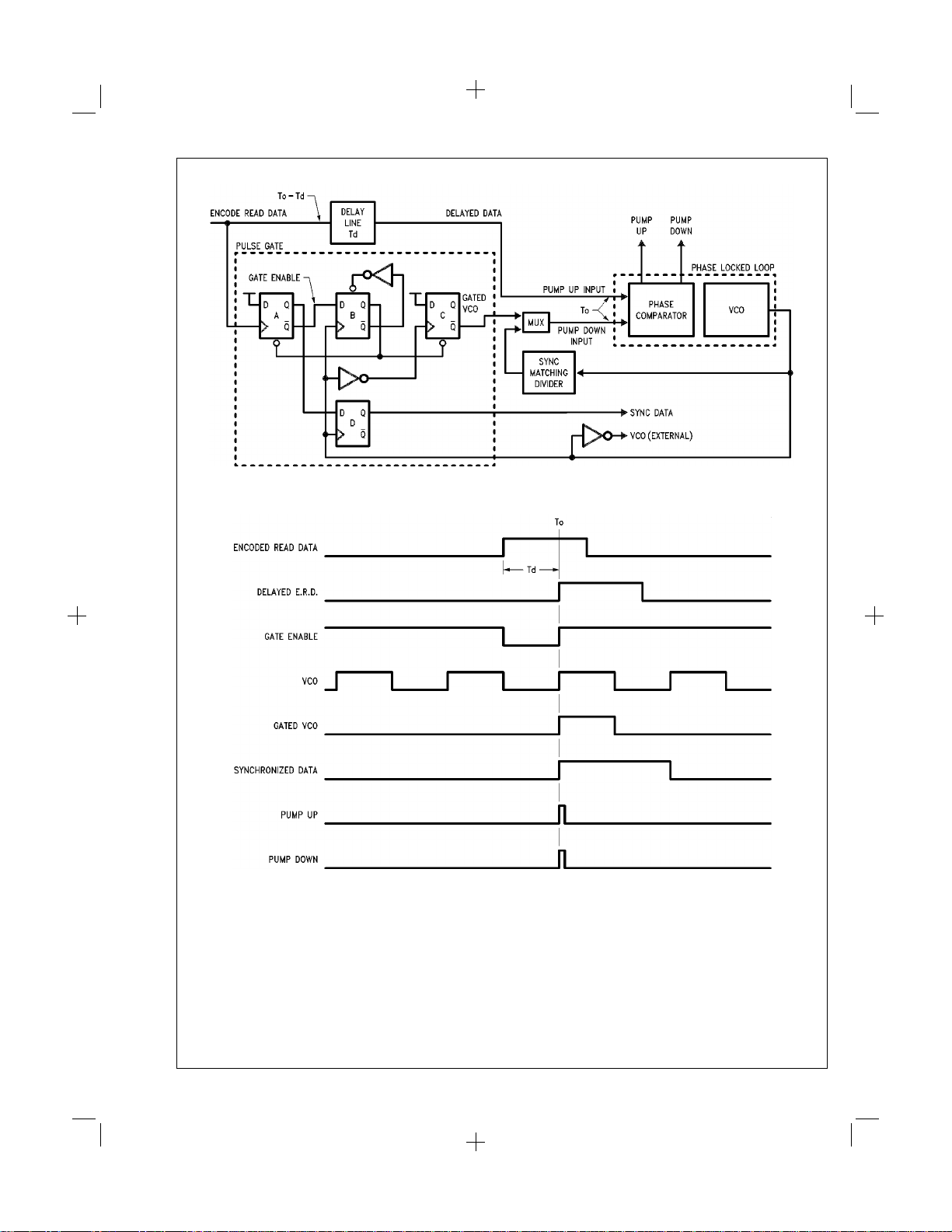
FIGURE 6. Simplified Diagram of Window Generation Circuitry
FIGURE 7. Capture of Nominally Positioned ENCODED READ DATA Pulse
TL/F/9322-11
TL/F/9322-12
10 http:\\www.national.com
PrintDate=1996/07/31 PrintTime=11:05:49 ds009322 Rev. No. 1 Proof 10
Page 11
FIGURE 8. Capture of Early-Shifted ENCODED READ DATA Pulse
FIGURE 9. Capture of Late-Shifted ENCODED READ DATA Pulse
DELAY LINE
The DP8459 employs an internal silicon delay line to establish
synchronization window alignment. The delay is nominally
equivalent to one half of the period of the REFERENCE
CLOCK waveform, and is variable in fine increments via the
TL/F/9322-13
TL/F/9322-14
Control Register in order to achieve the window strobe
function. The Timing Extractor circuitry derives realtive timing
information soley from the REFERENCE CLOCK signal and
regulates the magnitude of the delay within the Delay Line.
http:\\www.national.com 11
PrintDate=1996/07/31 PrintTime=11:05:49 ds009322 Rev. No. 1 Proof 11
Page 12

The Delay Line thus remains insensitive to the external
components associated with the extractor as well as to supply
voltage, temperature, and IC process variations.
TIMING EXTRACTOR
This block extracts timing information from the REFERENCE
CLOCK input for use by the variable silicon delay line. External
passive components (tied to the Timing Extractor Filter pin) are
associated with this block, although the accuracy of the
circuit’s function remains independent of the general value and
tolerance of the components. The resistor-capacitor net is
employed by the Timing Extractor for stabilization
purposes—no monostable multivibrator (one-shot) circuitry is
employed by the DP8459. Note that the performance of the
delay line is directly dependent upon the accuracy of the
REFERENCE CLOCK input waveform. Either a crystal
reference generator or a stable servo clock source must be
applied to this input. Multiplexing of the REFERENCE CLOCK
waveform between read operations (within multiple data rate
systems) is acceptable, although sufficient Timing Extractor
stabilization time must be allowed following any perturbation at
this pin before a read operation may be performed (see
10
for timing table).
Figure
PHASE COMPARATOR
The DP8459 employs a digital Phase Comparator
(non-harmonic discriminator circuit) which has the capability of
forcing the frequency of the PLL VCO toward the frequency of
the reference input regardless of the magnitude of the
frequency difference. The function of the Phase Comparator
circuit can be represented in a diagrammatically simplified
form as in
Figure 11
.
The Phase Comparator’s action can be disabled at any time
(cleared) via the COAST input pin, allowing the VCO to
free-run.
CHARGE PUMP
The Charge pump is a high speed, switching, dual-gain,
bi-directional current source whose current flow is controlled
by the digital Phase Comparator circuit. The current pulses at
the CHARGE PUMP OUTPUT (CPO) pin thus reflect the
magnitude and sign of the phase error seen at the input of the
Phase Comparator. The CPO pin is connected externally to a
passive component network whose impedance translates the
aggregate current into a voltage for the VCO INPUT while
providing a low-pass filter function for the PLL. The matched
source and sink current generators’ operating currents are set
via the R
from V
CC
R
NOMINAL
into each of these pins is internally multiplied by 2 for Charge
and R
NOMINAL
through external resistors. The bias voltages at the
and R
BOOST
pins, which are supplied current
BOOST
pins are set to 0.75 x VCC; the current
Pump use. The CPO current is defined as follows:
=
I
CPO
/2)/R
(V
CC
NOM
HIGH GAIN DISABLE high (logical-one)
=
I
CPO
/2)/(R
(V
CC
NOM
||R
BOOST
)
HIGH GAIN DISABLE low (logical-zero)
RFC Frequency 1 4 10 20 40 MHz
CT1 0.82 0.2 0.082 0.056 0.027 µF
RT1 68 68 68 68 68 Ω
Settling Time 192 96 19.2 9.6 4.6 µs
Values may be interpolated for intermediate data rates. Timing Extractor settling times are given which indicate time required for the DP8459 to accommodate a
change of Strobe setting from nominal selection to either extreme (early/late), or vice versa, to within approximately 1%of final value.
FIGURE 10. TIMING EXTRACTOR FILTER Component Values for Various Data Rates
TL/F/9322-17
FIGURE 11. Simplified Digital Phase-Frequency Comparator
VOLTAGE CONTROL OSCILLATOR (VCO)
The DP8459 VCO is comprised of two portions—a self
contained, high frequency oscillator (no external components)
whose frequency is regulated by the voltage at the VCO
INPUT pin, and a programmable modulus digital divider. The
oscillator is only required to operate over approximately a 2:1
frequency range; the divider modulus is programmable in
factors of 2. The two blocks work in conjunction to achieve a
continuous range of equivalent VCO operating frequencies
from 500 kHz to 50 MHz. (See
Figure 12.
)
CONTROL REGISTER
Within the DP8459, the Control Register is a MICROWIRE
compatible, 6-bit shift register block with bits 0 through 4
employed to control the window strobe function and bit 5
employed to regulate the device test mode (see
Figures 13
and14). Information is serially shifted into the Control
Register via the CRD and CRC (negative edge clock) pins
whenever the CRE pin is active (logical-zero). When the CRE
pin is inactive (logical-one), CRD and CRC are ignored.
Figure 3
shows the truth table for the VCO range select
function;
Figure 4
shows the truth table for the window strobe
function.
12 http:\\www.national.com
PrintDate=1996/07/31 PrintTime=11:05:51 ds009322 Rev. No. 1 Proof 12
Page 13

FIGURE 12.
FIGURE 13. Control Register
TL/F/9322-1
TL/F/9322-15
TL/F/9322-10
FIGURE 14. Microwire Compatible Control Register Serial Load Timing Diagram
SYNCHRONIZATION FIELD MATCHING DIVIDER
The Synchronization field Matching Divider is a programmable
modulus counter employed for implementation of the preamble
frequency lock function. It is placed in the VCO feedback path
to match the relative frequency of the VCO seen at the Phase
Comparator to the frequency of the ENCODED READ DATA
(preamble) during the read operation whenever the
FREQUENCY LOCK CONTROL input is active (logic-zero).
The modulus of the divider, M, is determined by the states of
the SYNC PATTERN SELECT 0 and 1 inputs, as defined by
the table in
Figure 15
.
Sync Pattern Sync Matching Expected
Code
Select Divider Modulus Preamble
10 M
0 0 1 GCR
0 1 2 MFM; 1,N
1 0 3 2,7
1 1 4 2,7
FIGURE 15. SYNC PATTERN SELECT Input Truth Table
Prior to the assertion of READ GATE, the divider is held in a
known count state and is enabled at the end of the zero phase
http:\\www.national.com 13
PrintDate=1996/07/31 PrintTime=11:05:52 ds009322 Rev. No. 1 Proof 13
Page 14

start sequence in correct phase relationship with the
ENCODED READ DATA. Re-assertion (logical zero) of the
FREQUENCY LOCK CONTROL pin within a read operation
(following the normal FLC deassertion after lock is achieved) is
permissible; however, it should be noted that the initial phase
error of the Synchronization Field Matching Divider with
respect to the ENCODED READ DATA at FREQUENCY-
LOCK CONTROL re-assertion may be as large as M x τ
in magnitude, possibly resulting in an extended PLL settling
VCO
time.
ZERO PHASE START
The function of the zero phase start (ZPS) block is to clear the
Phase Comparator and freeze the VCO in a known phase
when a transition occurs at the READ GATE input (either high
or low), and restart the VCO in a precise, controlled phase with
respect to the newly selected input (ENCODED READ DATA
or REFERENCE CLOCK
÷
2, respectively). The ZPS circuit
also resets the count state of the Synchronization field
Matching Divider in anticipation of locking to specific preamble
information (when frequency lock is being employed), and
controls the operation of the REFERENCE CLOCK
multiplexer. ZPS operation at READ GATE assertion is aimed
at optimizing initial window alignment and thus minimizing
initial phase step and the resulting phase lock acquisition time.
ZPS is also employed at deassertion of READ GATE;
however, the ZPS phase alignment for the REFERENCE
CLOCK signal at READ GATE deassertion has been made
less stringent than for ENCODED READ DATAat READ GATE
assertion.
PREAMBLE PATTERN DETECTOR
The Preamble Pattern Detector block has a pattern-specific
recognition circuit keyed to search the ENCODED READ
DATAfor the pattern selected at the SYNC PATTERNSELECT
inputs. The pattern search begins following the assertion of
READ GATE and the completion of the zero phase start
2.2 SPECIFICATION TABLES
Absolute Maximum Ratings
If Military/Aerospace specified devices are required,
please contact the National Semiconductor Sales
Office/Distributors for availability and specifications.
Supply Voltage 7V
TTL Inputs 7V
Output Voltages 7V
sequence, and continues until approximately 32 uninterrupted
ENCODED READ DATA pulses of the 1T, 2T or 3T pattern
have been detected, or until 16 uninterrupted ENCODED
READ DATApulses of the 4T pattern have been detected (see
specification tables). When this event occurs, the PREAMBLE
DETECTED output becomes active high (logical-one). The
output will then remain latched in the high state until READ
GATEis deasserted. The PREAMBLE DETECTED output may
be tied to the HIGH GAIN DISABLE input to regulate the gain
of the PLL during the preamble lock sequence, and/or tied to
the FREQUENCY LOCK CONTROL input for self-regulation
of frequency acquisition in hard or pseudo-hard sectored
systems.
±
50%VCO FREQUENCY OFFSET DETECTOR
The Frequency Offset Detector is employed to constrain the
VCO frequency swing, preventing VCO runaway associated
with standard, wide-range voltage controlled oscillators. The
circuitry will sense the relative difference between the
REFERENCE CLOCK frequency and the VCO frequency,
sending a “charge-up” signal to the Charge Pump to correct
the VCO should a limit of approximately −50%in frequency
differential (VCO w.r.t. REF CLOCK) be exceeded, and
sending a “charge-down” signal to the Charge Pump to correct
the VCO should a limit of approximately +50%in frequency
differential be exceeded.The resulting voltage-clampingaction
at the filter node(s) also prevents out-of-range control voltage
straying and thus speeds lock recovery.
SYNCHRONIZATION CLOCK OUTPUT MULTIPLEXER
This block issues the VCO signal following READ GATE
assertion and completion of the zero phase start sequence,
and issues the REFERENCE CLOCK input signal when the
READ GATE is deasserted. Multiplexer switching is achieved
without glitches. The output is intended to be used both for
read and write clock purposes. (Please note output loading
recommendations for this pin in Section 6.)
Input Current
(R
NOM,RBOOST
Storage Temperature −65
Operating Temperature Range 0
, CPO, VCOI, TEF) 2 mA
C to +150˚C
˚
Cto+70˚C
˚
ESD Susceptibility ( Note 3 ) 1500V
Operating Conditions
Symbol Parameter Conditions Min Typ Max Units
V
CC
T
A
I
OH
I
OL
V
IH
V
IL
f
NRZ
PrintDate=1996/07/31 PrintTime=11:05:54 ds009322 Rev. No. 1 Proof 14
Supply Voltage 4.75 5.00 5.25 V
Ambient Temperature 0 25 70
˚
High Logic Level Output Current SYNC CLOCK −2000 µA
Others −400
Low Logic Level Output Current SYNC CLOCK 20 mA
( Note 1 ) Others 8
High Logic Level Input Voltage 2 V
Low Logic Level Input Voltage 0.8 V
Operating Data Rate Range 0.25 25 Mb/s
14 http:\\www.national.com
C
Page 15

Operating Conditions (Continued)
Symbol Parameter Conditions Min Typ Max Units
t
PW-RFC
t
PW-ERD
Width of REFERENCE CLOCK, High or
8ns
Low
Width of ENCODED READ DATA 12 High ns
18 Low
t
PW-CRE
Width of CONTROL REGISTER ENABLE, 40 ns
High or Low ( Note 2 )
t
SU-CRD
CONTROL REGISTER DATA Set-Up Time 20 ns
with Respect to CRC ( Note 2 )
t
H-CRD
CONTROL REGISTER DATA Hold Time 10 ns
with Respect to CRC ( Note 2 )
t
H-CRE
t
SU-CRE
CONTROL REGISTER ENABLE Set-Up
20 ns
Time with Respect to CRC ( Note 2 )
CONTROL REGISTER ENABLE Hold Time 20 ns
with Respect to CRC ( Note 2 )
t
PW-CRC
I
CPIN
Note 1: PUMP UP and PUMP DOWN outputs have no current sinking capability and thus are excluded from this specification.
Note 2: Parameter guaranteed by correlation to characterization data. No outgoing test performed.
Note 3: Human body model; 120 picofarads through 1.5 kΩ.
CONTROL REGISTER CLOCK Pulse
Width, Positive or Negative ( Note 2 )
Combined R
NOM&RBOOST
Input Current 1000 µA
40 ns
AC Electrical Characteristics
Over recommended VCCand operating temperature range.
Symbol Parameter Min Typ Max Units
t
STOP
t
RESTART
t
READ ABORT
t
T
φ Linearity Phase Range for Charge Pump Linearity
K
VCO
f
MAX VCO
t
SD0
t
SD1
t
ZPSR
t
PWPC
∆f
VCO/fRFC
SYNC CLOCK Negative Transitions following READ
23—
GATE until Data Lock ZPS Sequence Begins (VCO
Freezes)
Positive ENCODED READ DATA Transitions following 2 —
VCO Freeze until VCO Restarts
Number of REF CLOCK Cycles following READ GATE
Deactivation until REF CLOCK Lock ZPS Sequence 4 —
Begins
Window Truncation (Half Window Loss);
DP8459V-10 10 Mbit/sec (Note 1 ) 3%x τ
DP8459V-25 20 Mbit/sec (Note 2 ) 4%x τ
±
VCO
VCO
π Radians
3.0 ns
2.5 ns
(wrt VCO)
VCO Gain Constant 1.0 ω
VCO Maximum Frequency; RS0=RS1=RS2
=
70 MHz
1.2 ω
O
1.6 ωORad/Sec V
O
Logical ZERO
Time Skew between SYNC CLOCK Negative Edge
010ns
and SYNC DATA Negative Edge
Time Skew between SYNC CLOCK Negative Edge
010ns
and SYNC DATA Positive Edge
Zero Phase Start Trigger Bit Targeting Accuracy,
2ns
READ GATE Activation (READ) ( Note 4 )
Width of PCT, PU or PD Outputs in Fully Stabilized 10 ns
Lock (ERD Free of Jitter); R-Pull-Down=510Ω
Automatic f
Range Limiting 50
VCO
http:\\www.national.com 15
PrintDate=1996/07/31 PrintTime=11:05:55 ds009322 Rev. No. 1 Proof 15
Page 16

AC Electrical Characteristics (Continued)
Over recommended VCCand operating temperature range.
Symbol Parameter Min Typ Max Units
t
HOLD
t
PDT
L
PDT1
L
PDT2
L
PDT3
L
PDT4
t
S
t
RFC–SCK1
SYNC CLOCK Rest Period (Logical One) at Assertion
or De-Assertion of READ GATE
SCK Negative Edge to PREAMBLE DETECTED
Positive Edge at End of Detection Sequence
Length of Valid 1T Preamble Pattern Required for
Occurrence of PREAMBLE DETECTED
Length of Valid 2T Preamble Pattern Required for
Occurrence of PREAMBLE DETECTED
Length of Valid 3T Preamble Pattern Required for
Occurrence of PREAMBLE DETECTED
Length of Valid 4T Preamble Pattern Required for
Occurrence of PREAMBLE DETECTED
Window Strobe Time Step (M=Hex Value of Bits 0–3
in CONTROL REGISTER; Bit 4=Sign Bit)
Positive Transition Propagation Delay from
REF CLOCK INPUT to SYNC CLOCK OUTPUT, 15 ns
READ GATE Low
t
RFC–SCK0
Negative Transition Propagation Delay from
REF CLOCK INPUT to SYNC CLOCK OUTPUT, 15 ns
READ GATE Low
Note 1: The DP8459V-10 static window specification, tT, applies only to the factory-tested 2,7-code data rate of 10 Mb/s (with RS0,1,2=010) and with the
component values as listed in Figures 5 and 10, test configuration as shown in Figure 23, test procedure as shown in Figure 24, and strobe word M=−2. Significant
variation in t
Note 2: The DP8459V-25 static window specification, t
of 20 Mb/s (with RS0, 1, 2,=000), with the component values as listed in Figures 5 and 10, test configuration as shown in Figure 23, test procedure as shown in
Figure 24, and strobe word M=−3. Significant variation in t
Note 3: I
Note 4: t
completion of a ZPS operation following READ GATE assertion.
as a percentage of the VCO period due to the use of other filters and data rates is not expected.
T
=
/(4xRIN). R
V
IN
CC
(ZPS Read) gauges the accuracy with which the ZPS circuitry aligns the VCO to the triggering ERD bit internally (i.e., initial phase step) at the
ZPSR
IN
=
R
NOM
(HGD High) or R
, incorporates the DP8459V-10 window specification and, in addition, the factory-tested 2,7-code data rate
T
as a percentage of the VCO period due to the use of other filters and data rates is not expected.
T
||R
BOOST
(HGD Low).
NOM
1
⁄
2
3T
VCO
25 ns
33 34 35
ERD
Pulses
32 33 34 ERD
Pulses
31 32 33 ERD
Pulses
15 16 17 ERD
Pulses
M x (1.8%)
xt
RFC
ns
DC Electrical Characteristics Over recommended operating temperature range.
Symbol Parameter Conditions Min Typ Max Units
=
V
IC
V
OH
V
OL
I
IH
I
IL
I
O
I
CPO
I
CPO-OFF
I
VCOI
V
RNOM
V
RBST
I
CC1
Note 1: This value has been chosen to produce a current that closely approximates one-half of the true short-circuit output current, IOS.
Note 2: I
Note 3: I
any given range selection. I
Most of the increase occurs as the −15 step is approached. I
Note 4: PUMP UP and PUMP DOWN outputs have no current sinking capability and thus are excluded from this specification.
Input Clamp Voltage V
High Level Output Voltage V
Low Level Output Voltage ( Note 4 ) V
High Level Input Current V
Low Level Input Current V
Output Drive Current ( Note 1 ) V
CC
CC
CC
CC
CC
CC
Charge Pump Output Current (K1) 100 ≤ IRp≤ 1000 (Note 2 ) 1.7 I
Charge Pump Output Inactive Current 100 ≤ IRp≤ 1000 (Note 2 ) −0.85 +0.85 µA
VCOI Offset Current VCOI Voltage 1.5V −0.25 +0.25 µA
Voltage across R-NOM Resistor 1.2 kΩ≤R-NOM ≤ 12 kΩ Typ.
Voltage across R-BOOST Resistor 1.2 kΩ≤R-BOOST ≤ 12
kΩ
Supply Current, Nominal Strobe V
=
I
Rp
NOM+IBOOST
is measured with the window strobe set at nominal timing (Strobe Bits 0 through 5=0,0,0,0,0,0); VCO operating at maximum allowed frequency within
CC1
.
typically increases by 30 mA when the strobe is set at the maximum early position (M=−15). This is not a linear increase per step.
CC
CC
decreases as the window is moved late.
CC
=
Min, I
−18 mA −1.5 V
I
=
=
=
=
=
=
Min, I
Min, I
Max, V
Max, V
Max, V
=
Max V
OH
=
Max 0.5 V
OL
=
2.7V 20 µA
I
=
0.4V −200 µA
I
=
2.125V −12 −110 mA
O
−2V VCC−1.6V V
CC
−18
Typ.
−18
2.0 I
Rp
0.26 V
%
0.26 V
%
2.5 I
Rp
CC
CC
Typ.
+18
Typ.
+18
Rp
%
%
Max (Note 3 ) 190 mA
16 http:\\www.national.com
µA
V
V
PrintDate=1996/07/31 PrintTime=11:05:57 ds009322 Rev. No. 1 Proof 16
Page 17

External Component Selection
Symbol Parameter Min Typ Max Units
R
NOM
R
BOOST
C
NOM
C
BOOST
R
PU
R
PD
Note 1: The minimum allowed value for the parallel combination of R
Note 2: C
NOM
Charge Pump Nominal Operating 1.2 12 kΩ
Current Setting Resistor ( Note 1 )
Charge Pump Boost Current 1.2
∞
Setting Resistor ( Note 1 )
R
Bypass Capacitor (Note 2 ) 0.01 µF
NOM
R
Bypass Capacitor (Note 2 ) 0.01 µF
BOOST
PUMP UP Open Emitter Output 510 Ω
Pull-Down Resistor
PUMP DOWN Open Emitter Output 510 Ω
Pull-Down Resistor
and C
should be high quality, high frequency type.
BOOST
NOM
and R
BOOST
is 1.2 kΩ.
kΩ
3.0 PLL Applications: Loop Filter Design
In order to maintain greatest design flexibility for the Customer,
all PLL filter components and Charge Pump gain setting
elements reside external to the DP8459. All PLL dynamics are
thus under the control of the system designer. The following is
a brief analysis of the DP8459 PLL; Section 3.1 contains a
derivation of component values based on projected
requirements within an example hard disk drive system.
Figure 16
represents the DP8459 PLL in simplified form.
FIGURE 16. Basic DP8459 Phase Locked Loop Block Diagram
N is defined as the number VCO cycles per recorded
ENCODED READ DATA pulse, or conversely, the ratio of the
VCO frequency to the ENCODED READ DATAfrequency.The
aggregate block gain equation (excluding the loop filter) can be
written as:
=
1.2 V
K
B
CCfO
/(2RpN)
The impedance of the loop filter is
Mathematical gain representations for each block are:
=
K
1/N Pulse Gate equivalent gain
PG
=
1/(2π) Phase Comparator gain
K
PC
=
/2RpCharge Pump gain where R
V
K
CP
CC
HGD high; R
=
K
VCO
frequency)
<<
If C
C1, the impedance Z(s) approximates to
2
p
1.2 ω
=
R
NOM
O
||R
, HGD low
BOOST
VCO gain (ω
O
p
=
operating center
TL/F/9322-18
The overall open loop gain (including the filter) is then
=
,
R
NOM
Substituting KBinto the equation,
The open loop system response G(s) is given by
This last equation reveals the PLL with this filter configuration
is a third order system, which is typically difficult to analyze.
However,if C
third order loop closely resembles that of a second order
<<
C1, it can be argued that the behavior of the
2
=
τ
R
1
pC1
which govern the system response. The closed loop gain H(s)
is
and τ
=
are the pole and zero, respectively,
R
2
1C1
system, allowing for a greatly simplified analysis.
http:\\www.national.com 17
PrintDate=1996/07/31 PrintTime=11:06:00 ds009322 Rev. No. 1 Proof 17
Page 18

Substituting,
The second order characteristic equation can be written as
follows:
2
s
+sKBR1+KB/C
=
1
2
+s2ζωn+ ω
s
2
n
Extracting the component values from these results,
Thus, one is able to select component values in accordance
with specific system requirements, i.e., with given VCO center
frequency (equivalent to REFERENCE CLOCK frequency), R
(in either high or low gain mode), N (the ratio of the VCO
frequency to the ENCODED READ DATA frequency), the
desired natural frequency of the loop, and the desired damping
ratio.
The natural frequency and the damping ratio may be extracted
from the component values to determine system behavior
under various conditions (differing data patterns, i.e., varying N
value; high gain or low gain; read or non-read mode):
=
ω
[1.2 V
n
CCfo
/2RpNC1)]
0.5
Natural frequency Damping ratio
nR1C1
/2
ζ=ω
3.1 2,7 CODE, 10 MBIT/SEC LOOP FILTERDESIGN
EXAMPLE
Initial Requirements and Definitions
This example illustrates a 10 MBit/sec 2,7 hard disk system
employing a 4T preamble field (recorded at
1
frequency, i.e., N=4). The component derivations are not
meant to produce values which will be optimum for all systems
employing this data rate, code, and preamble type; this
exercise is for exemplary purposes only. (See National
Semiconductor Advanced Peripheral Processing Solutions
Mass Storage Handbook
#
1, 1986,AN-413, section 3.4, pages
1-43 through 1-48 for additional information regarding disk
system PLL filter design.)
Although the DP8459 provides a frequency acquisition feature
intended for use within the preamble, this design example will
be approached so as to achieve PLL dynamics which will avoid
the cycle-slipping phenomenon frequency-lock action is
normally employed to accommodate. Thus, the design will be
valid both for systems which do employ frequency lock as well
as for those which do not. Advantages gained by the use of
frequency-lock beyond that of extended lock-in range,
however, such as harmonic false lock avoidance and
quadrature lock avoidance, make the use of this feature
p
strongly advisable even with the intrinsic lock-in range
achieved by design in this example.
The DP8459 is configured here with the FREQ LOCK CONTROL input tied to the PREAMBLE DETECTED output, the
HIGH GAIN DISABLE input tied to the READ GATE input, and
the CHARGE PUMP OUTPUT tied to the VCO INPUT pin as
well as to the external loop filter components (see
This establishes self-regulated frequency lock control, READ
GATE regulated Charge Pump gain, and single node loop
filtering.
⁄4the VCO
Figure 17
).
18 http:\\www.national.com
PrintDate=1996/07/31 PrintTime=11:06:01 ds009322 Rev. No. 1 Proof 18
Page 19

FIGURE 17. DP8459 in a Typical System Configuration
System constraints:
f
f
f
Code type
N
N
N
=
NRZ DATA
VCO
REFERENCE CLOCK
min
max
preamble
10 Mbit/sec
=
20 MHz
=
3 (highest recorded frequency)
=
8 (lowest recorded frequency)
=
=
4(f
1
⁄2(2, 7)
preamble
=
20 MHz
=
5 MHz)
Preamble Length=11 NRZ bytes (ESDI min.)=8.8 µs
(44 recorded pulses)
Disk formatting=pseudo hard sectored
The DP8459 provides a zero phase start function which
minimizes the initial phase step encountered at the start of
preamble lock acquisition and thus the phase stabilization time
within the preamble is significantly reduced with respect to a
fully random-phase lock sequence. However, the PLL will
encounter a finite frequency step at the start of preamble
acquisition due to variations in disk rotational velocity which
may be as large as
±
1%(more pronounced in exchangable
media systems). The lock-in range of the PLL at the time of
preamble acquisition must then be at least
Given that the PLL lock sequence involves only an adjustment
±
0.01 x f
preamble
.
to a frequency step, the following requirements will be set for
final PLL dynamics within the filter design procedure:
http:\\www.national.com 19
TL/F/9322-19
1. Residual phase error θ
NRZ bytes allowed for PLL stabilization) will be 2 ns or less
at the end of the preamble (a full 11
e
(4%of the total synchronization window).
2. The lock-in range ∆ω
expected frequency step range.
3. The minimum 3 dB bandwidth ω
be twice the expected maximum mechanical vibration
must be at least 1.5 times the
L
in the data field must
−3 dB
frequency (10 kHz).
4. The natural frequency of the loop ω
will be minimized in the data field in order to achieve a high
and damping ratio ζ
n
level of jitter rejection. (Minimum damping ratio ζ will be 0.5
(phase margin of 52
) for adequate stability).
˚
5. Re-lock time to the REFERENCE CLOCK will be
minimized.
First, some definitions will be established. Regarding
requirement
frequency step are
(t)=[ ∆ω/ωn] [1/(1–ζ2)
θ
e
(t)=[∆ω/ωn] [1/(ζ2−1)
θ
e
These equations are plotted in
phase error due to a phase step are
#
1, the equations for phase error due to a
1
:
0.5
sin(1−ζ2)
0.5
ωnt]exp(−ζωnt) for ζ
1;
(t)=[ ∆ω/ωn][ωnt]exp(−ωnt) for ζ=1;
θ
−[ζ/(1−ζ
e
2)0.5
0.5
sinh (ζ2−1)
>
for ζ
Figure 18
(t)=∆θ{ cos (1−ζ2)
θ
e
] sin (1−ζ2)
0.5 ω
1.
1
:
0.5
nt} exp(−ζωnt) for ζ<1;
0.5
ωnt] x exp(−ζωnt)
. The equations for
ωnt
<
PrintDate=1996/07/31 PrintTime=11:06:03 ds009322 Rev. No. 1 Proof 19
Page 20

θe(t)=∆θ[1−ωnt]exp(−ωnt) for ζ=1;
(t)=∆θ {cosh(ζ2−1)
θ
e
2
[ζ/(ζ
−1)
0.5
]sinh(ζ2−1)
0.5
ωnt}exp(−ζωnt) for ζ>1.
0.5
ωnt−
(These equations are plotted in
informational purposes only; an ideal zero phase start function
would not produce a phase step at lock initiation.)
FIGURE 18. Transient Phase-Error Versus the Dimensionless Parameter ω
Loop Damping Factors, ζ (from Ref. 4 by Permission of L. A. Hoffman)
Figure 19
t Due to a Step in Frequency for Various
n
and are supplied for
TL/F/9322-20
TL/F/9322-21
FIGURE 19. Phase-Error Versus the Dimensionless Parameter ω
Factors, ζ (from Ref. 4 by Permission of L. A. Hoffman)
Note that the phase error θ
divided (or gated) VCO phase, i.e., 2π radians=N/(20 MHz)
is measured with respect to the
e
=
200 ns in this example.
t Due to a Step inPhase for Various Loop Damping
n
Regarding requirement
#
2, the lock-in range (with no
cycle-slipping) can be shown to be equal to the open loop
transfer function multiplied by the loop filter impedance
evaluated at infinite frequency
20 http:\\www.national.com
∆ω
2
:
≈
±
KBZf(s)|
→
L
∞
s
PrintDate=1996/07/31 PrintTime=11:06:04 ds009322 Rev. No. 1 Proof 20
Page 21

The 3 dB bandwidth for requirement#3 is defined by the
3
equation
:
ω
−3 dB
=
[2ζ2+ 1 +{(2ζ2+1)2+1}
ω
n
0.5]0.5
Requirement#4 has been established in order to maximize the
available window margin via PLL dynamics. Conceptually,
window margin is preserved if the loop phase response to
individually displaced bits (jitter) is not allowed to cause
subsequent windows to be readily shifted from the “average”
position. Any window movement from nominal position can
readily degrade the window margin. It can be seen from
19
that systems employing low values of damping ratio exhibit
Figure
a reduced instantaneous response to phase step and thus
display improved jitter rejection with respect to higher damping
ratio systems. Damping ratio, fortunately, is easily regulated by
loop filter design. It also follows that a low natural frequency
and its associated “slower” instantaneous phase response will
assist in achieving the goal of jitter rejection. However, the
minimum natural frequency limit for the PLL may actually be
imposed on the system by the θ
the ∆ω
requirement, or the ω
L
these produces the highest minimum ω
necessity, dominate in the design. The goal of minimizing the
(t) settling time requirement,
e
requirement. Whichever of
−3 dB
value must, by
n
natural frequency in order to maximize jitter rejection,
therefore, may have to defer to one of these other three
criteria.
Requirement
#
5 is addressed in three ways: 1) the DP8459
itself engages the frequency discriminating action of the Phase
Comparator whenever the READ GATEis deasserted and the
PLL locks to the REFERENCE CLOCK signal, thus
guaranteeing re-lock regardless of the initial frequency step; 2)
tying the HIGH GAIN DISABLE pin to the READ GATE input
places the Charge Pump in the high gain mode whenever the
PLL is locked to the REFERENCE CLOCK, producing an
elevated natural frequency and a more rapid locking action; 3)
N=2 whenever the READ GATE is deasserted, which, in this
example, effectively increases the loop gain by another factor
of 2 with respect to the gain within the preamble, where N=4.
Determining PLL Response Characteristics
It is expected that the minimum value of ω
by the residual phase error requirement of
lock-in range requirement of
#
3. This assumption will be checked at the end of the analysis.
#
2ortheω
will be determined
n
#
1 rather than the
requirement of
−3 dB
System requirements then are as follows:
1. θ
(t) ≤ (2 ns) x (2π rad/ 200 ns)=0.063 radians,
e
where t=preamble length 8.8 µs
≈
±
2. ∆ω
3. ω
L
−3 dB
KBZf(s)|
=
ω
n
≥ 0.015x5MHzx2π=471 Krad/sec
→
∞
s
[2ζ2+1+{(2ζ2+1)2+1}
0.5]0.5
≥ 2x10kHzx2π=126 Kr/s
#
Requirement
1 calls for θe(8.8 µs) ≤ 0.063 radians. Damping
ratio ζ varies as the inverse square root of N (see the equation
for Damping Ratio in Section 3.0) such that ζ
√
(N
MAX/NPREAMBLE
appropriate equation for θe(t) for various values of ωnwith ζ
)xζ
=
√
2 x 0.5=0.707. Solving the
MIN
PREAMBLE
0.707, t=8.8 µs and an expected frequency step of 0.01 x 5
MHzx2π=314 Kr/s:
ω
n
θe(8.8 µs) |te|
200 Kr/s 0.606 rad 19.29 ns
300 Kr/s 0.219 rad 6.97 ns
400 Kr/s 0.056 rad 1.78 ns
500 Kr/s 0.0012 rad 0.038 ns
600 Kr/s −0.0098 rad 0.312 ns
ω
n
θe(8.8 µs) |te|
700 Kr/s −0.008 rad 0.026 ns
400 Kr/s
=
0.056 radian
(8.8µs)|
θ
e
=
t
0.056 radian x 200 ns/2π radian=1.78 ns
e
<
0.063 radian
Thus 400 Kr/s is chosen as the desired natural frequency
within the preamble to satisfy requirement
If the assumption that θ
frequency requirement is correct, then the ∆ω
#
2 and the ω
obtained above. First, examining requirement#2,
−3 dB
Z
(t) dominates the minimum natural
e
requirement of#3 should be met by the ω
=
f
(s)|
R
→
∞
s
1(C2
#
neglected).
1.
requirement of
L
Thus,
=
K
∆ω
L
BR1
Rearranging for R1:
=
R
∆ω
1
L/KB
The equation for R1previously derived shows
=
R
2ζω
1
n/KB
Thus,
=
∆ω
=
In this case, ω
∆ω
L
Thus, requirement
400 Kr/s and ζ=0.707 (preamble), thus
n
=
400Kr/sx2x0.707=566 Kr/s
#
2 is met.
Examining requirement
when N equals its maximum value of 8 (minimum frequency
2ζω
L/KB
=
∆ω
2 ζωn
L
#
3, where ω
n/KB
>
≥ 2x10kHzx2π
−3 dB
471 Kr/s
data pattern; ζ=0.5):
ω
(min)=ωn(preamble) x 1/√(N
n
=
400 Kr/s x 1/
=
ω
ω
−3 dB
n(min)
=
283 Kr/s x 1.817=514 Kr/s
514 Kr/s
Thus requirements
the minimum ω
#
established by#1.
n
Regarding requirement
[2ζ2+1+{(2ζ2+1)2+1}
÷
2π=82 kHz>2x10kHz
1 through#3 are met, and#4 defers to
#
5, the DP8459 has been configured
MAX/NPREAMBLE
√
2=283 Kr/s
externally in this example such that when the READ GATE is
deasserted, the loop gain will be increased by a factor of 2 due
to the Charge Pump gain switching (R
tied to RG) and by an additional factor of 2 due to the decrease
NOM
=
R
in N from 4 (preamble) to a fixed internal value of 2. The
resulting factor of 4 effective gain elevation results in an
increase in both the natural frequency, ω
ratio, ζ,by
√
4=2. Thus, when READ GATE is deasserted,
=
ω
2 x 400 Kr/s=800 Krad/s
n
, and the damping
n
ζ=2 x 0.707=1.414
=
=
2ζω
∆ω
L
=
COMPONENT CALCULATIONS
The formulae for the filter components, derived previously, are
=
2 x 1.414 x 800 Krad/s=2.3 Mr/s
n
A 2:1 ratio of high-to-low Charge Pump gain was chosen for
the derivation of R
ratio, R
must be equal to R
NOM
NOM
and R
. To achieve the 2:1 gain
BOOST
while the parallel
BOOST
0.5]0.5
BOOST
<
2ns
n
)
; HGD
http:\\www.national.com 21
PrintDate=1996/07/31 PrintTime=11:06:07 ds009322 Rev. No. 1 Proof 21
Page 22

combination R
1.2 kΩ as per specification. Note that in the equation for C
NOM
||R
must be equal to or greater than
BOOST
above, the capacitor value is inversely proportional to Rp.
R
can now be calculated:
1
1
Thus, external field interference immunity can be achieved if
C
is maximized through the minimizing of Rp. The selection of
1
=
R
NOM
Charge Pump resistors and the gain ratio. R
R
with READ GATE high, and thus
NOM
=
C
[1.2x5x20MHz/(2 x 2.4k x 4)]/(400 Kr/s)
1
=
0.039 µF
R
=
2.4 kΩ satisfies the requirements for the
BOOST
will be equal to
p
2
A standard value of 100Ω is chosen. Since C2≤ 0.1xC1,C
will be chosen to be 510 pF. A table listing the dynamics of the
PLL under standard operation conditions and with component
values adjusted to industry standards is shown in
Figure 20
Field Preamble Min Freq Data Max Freq Data Ref Clock
N4 8 3 2
CP Gain Low Low Low High
Natural
Freq. 400 Krad/s 283 Krad/s 462 Krad/s 800 Krad/s
ω
n
Damping
Ratio 0.7 0.5 0.8 1.4
ζ
FIGURE 20. 2,7 Code, 10 Mbits/Sec Design Example PLL Dynamics
4.0 Window Margin and Bit Jitter Tolerance
A key performance specification for the DP8459 involves the
integrity of the synchronization window. The synchronization
window is defined as a continuously repeating time cell,
nominally equal in span to the period of the VCO, within which
an ENCODED READ DATA pulse will be recognized
(captured) regardless of its position within the window (see
Figure 21
). The captured ERD bit is then transmitted to the
SYNCHRONIZED DATA output on the next occurring SYNC
CLOCK negative edge. The SYNCHRONIZED DATA and the
SYNC CLOCK are held in a fixed, specified timing relationship
for use by the data controller in deserialization and decoding.
position) is centered about the mean location of the ERD
pulses via the delay line and the time-averaging action of the
PLL. National Semiconductor specifies the static window
truncation (t
maximum expected loss of the synchronization window seen
) of the DP8459 data synchronizer as the
T
adjacent to the ideal window boundary following complete PLL
stabilization with the strobe control setting at the M=−2
position (see
Figure 22
). Static lock conditions are defined as
having been achieved when the PLL has been allowed to
establish fully stabilized lock to a consistent preamble-type
pattern of nominally positioned, non-shifted ERD pulses.
The synchronization window (with strobe setting at nominal
2
.
TL/F/9322-22
FIGURE 21. Synchronization Window
22 http:\\www.national.com
PrintDate=1996/07/31 PrintTime=11:06:08 ds009322 Rev. No. 1 Proof 22
Page 23

FIGURE 22. Window Specification Diagram
4.1 SYNCHRONIZATION WINDOW GENERATION
The DP8459 employs a pulse gate-delay line scheme in the
generation of the synchronization window.
Figure 6
shows a
simplified block diagram of the pulse gate and delay line
circuitry coupled with the phase locked loop. All elements
except the delay line are assumed to be delayless for
simplicity of analysis. The pulse gate allows a single VCO
edge to be transmitted to the pump down input of the phase
comparator for each arriving ENCODED READ DATA pulse,
while the delay line allows the ENCODED READ DATA pulse
to open (enable) the pulse gate at a predetermined time (t
prior to the arrival of the ERD pulse at the pump up input of the
phase comparator.
Figures 7, 8
and9show waveform
diagrams of the capture of nominal, early and late ERD pulses,
respectively. In normal operation where stable lock has been
achieved, the time-integrating action of the PLL has
established time alignment between the waveforms at the
phase comparator inputs, i.e., both events occur at t
,on
o
average. If t
ERD pulse will open the pulse gate at t
the midpoint between VCO edges. ERD pulses are then free to
is set equal to 0.5 x τ
d
, the nominal or average
VCO
− 0.5 x τ
o
VCO
shift to any position (ideally) between VCO edges, that is, they
have an allowed displacement of
while yet opening the pulse gate for the passing of the
±
0.5 τ
from the mean,
VCO
appropriate VCO edge to the phase comparator and at the
same time being properly captured by the data synchronization latch (flip-flop D,
referred to as the synchronization (capture) window.
Any variation in the value of the time delay t
)
d
at which the pulse gate is enabled (t
VCO waveform midpoint, and thus produces a corresponding
Figure 6
). The±0.5 τ
causes the time
d
) to shift away from the
o–td
VCO
shift in the position of the synchronization (capture) window.
This action, when done in a controlled fashion, is known as
window strobing and is useful for purposes of window skew
compensation, determination of system window margin, and
recovery routines for non-readable data (see Section 4.3).
TL/F/9322-23
, precisely
region is
http:\\www.national.com 23
PrintDate=1996/07/31 PrintTime=11:06:09 ds009322 Rev. No. 1 Proof 23
Page 24

Notes: SD and SCK outputs are buffered by Advanced Schottky gates to provide standardized, typical loading conditions.
CRC, CRD, CRE, RG, and ERD are driven by a pattern generator providing the appropriate sequences both to load the control register with the appropriate
strobe position information and to cycle the RG and ERD test routine as per
Figure 24
.
TL/F/9322-24
FIGURE 23. DP8459 Window Measurement Configuration
4.2 WINDOW TRUNCATION TESTING
The DP8459 static window truncation specification is an
aggregate figure within which the window margin loss
contributions from all relevant blocks in the data synchronization chain are combined into the single parameter, t
.
T
The preliminary DP8459 static window specification, t
applies only to the factory-tested data rates of 10 Mb/s
(with RS0,1,2=010) and 20 Mb/s (with RS0,1,2=000), with
the component values as listed for each corresponding
data rate in
in
Figure 23,
Figures 5,
and
10,
test configuration as shown
test procedure as shown in
Figure 24,
strobe word M=−2 for 10 Mbits/sec and M=−3 for 20
Mbits/sec. Significant variation in t
other filters and data rates is not expected.
due to the use of
T
The test algorithm employed in the outgoing factory
measurement (screening) of t
DATA stream consisting of a long synchronization field with a
emulates an ENCODED READ
T
single, movable test bit at its end. This method is referred to as
static
window testing, since the window in which the test bit is
inserted is fully stabilized and unable to react instantaneously
to the phase step introduced by the displaced bit. The standard
screening procedure employed for determining DP8459 static
window truncation is divided into two portions, one which
determines the location of the leading (front) window boundary
and one which determines the trailing (back) window
center of the target window until it resides in a position where
it is able to be detected a large number of times consecutively,
guaranteeing VCO jitter immunity. The time displacement
between the bit’s valid detection position and the ideal leading
window boundary is recorded as t
negative if the actual window boundary resides outside the
,
T
ideal window.) The variable bit is then placed outside the
(front). (This value may be
Tf
trailing window boundary and the variable bit is again moved,
once per read cycle, from outside the target window across the
ideal boundary and into the window. The bit continues to
advanced toward the center of the recognition region until it is
and
in a position where it is able to be read a large number of times
consecutively. The time displacement between the bit’s valid
detection position and the ideal trailing window boundary is
recorded as t
actual window boundary resides outside the ideal window due
(back). (Again, the value may be negative if the
Tb
to window encroachment.) The larger (more positive) of the
two (t
sequence is shown in
) values is taken as tT. A flow chart of the test
Tf,tTb
Figure 24.
Tables of external component
values used for production screening of the DP8459 at various
data rates are shown in
Figures 5
and
10.
Window truncation evaluated within data patterns containing
shifted bits is a direct function of PLL dynamics which are
under Customer control, and thus is neither tested nor
specified.
boundary. The DP8459 is made to cycle through the read
operation many times as a variable bit is moved, once per read
cycle, from outside the target window across the ideal leading
boundary and into the window.The bit is advanced toward the
24 http:\\www.national.com
PrintDate=1996/07/31 PrintTime=11:06:10 ds009322 Rev. No. 1 Proof 24
Page 25

4.3 WINDOW STROBE
The DP8459 incorporates a window strobe function capable of
shifting the synchronization window either early or late with
respect to its nominal position in small, specified steps. The
strobe step t
the DP8459 synchronization window from its nominal (strobe
is defined as the controlled time displacement of
S
centered) position and is typically
=
t
M x [1.8%x τ
S
VCO
]
where M is the value of the strobe control word (−15 through
+15; see
Figure 4
) set by the first 5 bits within the Control
Register.(Note that M is equivalent to the hexidecimal value of
the five strobe control bits where bits 0 through 3 are the LSB
through MSB and bit 4 is the sign bit.)
The changing of the strobe value t
event following the changing of the control word in the Control
is not an instantaneous
S
Register. The response time of the strobe control circuitry to
any change in strobe setting is a function of the timing
elements connected to the TIMING EXTRACTOR FILTER pin
and the data rate at which the device is being operated.A finite
settling time must be allowed for the delay circuitry to respond
following the loading and latching of the new control word
(latching occurs and strobe changes begin at de-assertion of
CONTROL REGISTER ENABLE, i.e., at transition to logical
ONE). It is recommended that any changes to the strobe
setting be done with READ GATE deasserted and with a
sufficient allowance for settling time prior to the initiation of a
subsequent read operation. Approximate settling times are
given in
Figure 10
for various TEF component values at
specific data rates. (Please refer to AN-578 Window Strobe
Function.)
4.3.1 MARGIN TESTING
The read channel window margin of a disk/tape memory
system is the portion of the synchronization window remaining
after the subtraction of all possible sources of degradation
such as media bit shift, head-amplifier anomalies, pulse
detector anomalies, cable-induced skew,synchronizer losses,
and extraneous noise. The remaining margin must be
sufficient to allow the system to perform with an acceptable
media error rate under all operating conditions. Acceptable
media error rates will vary between systems depending on
ECC codes, data redundancy, and other factors. The
measured value of the synchronization window margin is often
used as a performance criteria for HDA (head-disk assembly)
and read channel qualification, and for gauging the probability
of encountering data errors on the media.
The DP8459 strobe function can be readily used to measure
the window margin within a drive system. Margin tests have
been most frequently employed only during outgoing factory
tests of storage media systems with specialized and costly test
apparatus employed for the purpose; however, the DP8459
allows media/system qualification at any time in the factory or
the field during the system’s operational life, given the
incorporation of an appropriate margin test algorithm within the
disk system controller. The algorithm may be configured first to
record the most bit-interactive (shift-producing) pattern
possible with the recording code being employed (eg., a
repeating hex 6D B6 pattern in MFM) in an area of the media
where recording density is its highest (inner-most track in
constant-angular velocity or constant data rate disk systems),
and secondly to read the track repeatedly while incremently
advancing the degree of window “strobe” (controlled shift) first
in the early direction until the data error rate crosses a
pre-determined threshold and then in the late direction until the
same threshold is again crossed. The smaller of the two
DP8459 window strobe measurements (either the early or the
late value) determined at the error rate threshold crossing
points is then equal to the read channel window margin.
http:\\www.national.com 25
PrintDate=1996/07/31 PrintTime=11:06:11 ds009322 Rev. No. 1 Proof 25
Page 26

TL/F/9322-25
FIGURE 24. DP8459 Static Window Truncation Test Flow Chart
4.3.2 ERROR-BOUND SECTOR/TRACK DATA RECOVERY
A standard technique exists for attempting to recover illegible
data from a sector or track within a disk system which involves
the re-reading of the bad data while shifting the data
synchronizer window a small amount early/late with respect to
the nominal position. A typical early/late strobe value for data
retrieval is in the range from approximately 2%to 3%of the
total window width. The strobe step size produced by the
DP8459 window control circuitry easily allows for this type of
data recovery procedure, and is in fact small enough to
feasibly permit more than one degree of window movement
within the data recovery algorithm.
4.3.3 AUTO WINDOW ALIGNMENT (DE-SKEW ROUTINE)
It is possible to configure an intelligent drive system to employ
the DP8459 strobe feature in a window auto-calibration
(de-skew) routine implemented to center the detection window
about the mean position of the bit distribution curve. The
de-skew routine would maximize the read channel window
threshold crossing points would be numerically combined to
determine the window center skew.For example, if at 10 Mb/s
the strobe-until-error value in the “early” direction were found
to be M=−8 and the “late” value M=4, window skew would
be determined as follows:
=
t
skew
1.8 x τ
=
x[M
VCO
early+Mlate
0.9 ns x [−8 + 4]/2
=
− 1.8 ns
]/2
The window has an apparent shift of 1.8 ns in the late
direction. The strobe setting in the DP8459 would then be set
to compensate for the skew, centering the synchronization
window and maximizing the available read channel window
margin. In this case, the strobe setting would be M=−2. This
routine could be executed at system power-up and perhaps on
a regular, specified time schedule during system operation to
maintain a fine-tuning of the read channel timing
characteristics under varying operating conditions (conceiv-
ably eliminating the need for an error-strobe routine).
margin and correspondingly minimize the bit error rate (BER).
The auto-calibration routine would be configured as an
extension of the window margin routine (Section 4.3.1), where
the early and late strobe values determined at the error rate
26 http:\\www.national.com
PrintDate=1996/07/31 PrintTime=11:06:12 ds009322 Rev. No. 1 Proof 26
Page 27

Original Window Position
TL/F/9322-2
Early Strobe Window Position
TL/F/9322-3
Late Strobe Window Position
TL/F/9322-4
De-Skewed Window Position
TL/F/9322-5
5.0 Multiple Data Rate Applications
The DP8459 may be rapidly and easily switched from one data
rate to another, conceivably from its highest to its lowest
specified data rate and vice versa, with a minimum of
adaptation effort. This capacity facilitates the employment of
the DP8459 for stepped data rate disk applications (constant
density recording, or CDR), or for the employment of a single
data synchronizer for multiple-media controllers as a cost and
space conserving measure, e.g., allowing a controller to
address tape, floppy disk and hard disk read channels on a
multiplexed basis while employing a single data separator.
DP8459 data rate changes require only the appropriate new
REFERENCE CLOCK frequency be applied and the
necessary new RANGE SELECT information be presented to
the chip in cases where the Customer chooses to employ
compromise loop and Timing Extractor filters. The Customer
may alternatively choose to employ a transmission gate
technique to multiplex between appropriate filter elements for
various operating data rates should the frequencies be
sufficiently different (e.g., streaming tape drive versus hard
disk drive).
6.0 PC Board Layout Recommendations
The DP8459 data synchronizer circuit has been designed to
minimize the sensitivities normally associated with phase
locked loops which operate within digital environments, and in
particular those within disk and tape memory systems. A list of
recommendations and precautions is made available here for
the Customer, however, such that the DP8459 environment
can be optimized and the best possible performance achieved
with the device.
1. A localized V
for the device and all its associated passive components,
supplied by but separated from the main V
local V
one point and bypassed to the ground plane at that point.
2. The DP8459 V
through the shortest electrical path possible between the
supply net or island should be established
CC
plane. The
net should be tied to the main VCCplane at only
CC
pins should be bypassed to ground
CC
CC
supply pins the ground pins themselves. Bypassing should
be achieved with a 0.1 µF ceramic capacitor in parallel with
a 1000 pF silver mica capacitor.
3. The main digital ground plane should be used for all
grounding associated with the device. Both Analog and
Digital ground pins should be tied to this plane.
4. All passive components associated with the DP8459
should be located as close to their respective device pins
as possible. Lead length should be minimized.
5. External passive components should be oriented so as to
minimize the length of the ground-return path between the
component’s ground plane tie point and the DP8459 Analog
ground pin.
6. In order to minimize pin parasitic capacitances, planing
(supply or ground) should not be placed between device pin
eyelets.
7. Digital signal lines should not be run adjacent to external
passive analog components associated with the device.
Digital signal lines should not be run between analog signal
pins or traces associated with the device.
8. Digital input noise experience by the device should be
minimized, i.e., it may be advisable to condition input
waveforms in order to reduce transient noise. This may be
done with a series damping resistor at the REFERENCE
CLOCK input (and perhaps at the ENCODED READ DATA
input) in high frequency systems. This would terminate
board traces and thus prevent under-damped,
noise-producing switching transients at the device inputs.
9. Digital output loading should be minimized, i.e., if outputs
must drive large loads or long traces, employ buffering.
Pre-termination of PC traces driven by the SYNCHRONIZED CLOCK and SYNC DATAoutputs may be advisable
in high frequency systems (i.e., include series resistance
equivalent to the characteristic impedance of the PC board
trace).
10. All unused digital output pins should be allowed to float,
unconnected to any trace.
11. The device should not be located in a region of the PC
board where large V
or ground plane currents are
CC
http:\\www.national.com 27
PrintDate=1996/07/31 PrintTime=11:06:13 ds009322 Rev. No. 1 Proof 27
Page 28

expected, or where strong electric or magnetic fields may
be present. The lowest ambient noise region of the board
should be chosen for device location.
12. If device socketing is desired, a low-profile, low mutual
capacitance, low resistance, forced-insertion socket type
should be employed.
13. Wire-wrapping should not be employed, even in an
evaluation set-up.
14. Capacitors used for the loop filter, the Timing Extractor
filter, and all bypassing purposes should be ultra-stable
monolithic ceramic capacitors or equivalent timing quality
capacitors. Silver-mica capacitors should be employed for
values 1000 pF and below.
15. In order to achieve very close proximity of passive
components to the DP8459 device, it is acceptable to
have axial-lead resistors standing upright; however, the
shorter component lead should be connected to the
device pins to obviate noise induction into sensitive
nodes.
7.0 Application Support
It is National Semiconductor’s policy to offer and maintain a
high level of direct Customer support on all of its mass storage
products. National’s experience in supporting the disk data
memory industry has allowed the DP8459 to be designed to
directly address the unique challenges of serial data
synchronization within the areas of magnetic and optical media
data storage and local area networks, facilitating straightforward use of the device in a diverse rangeof applications.In the
event that questions arise regarding the use of the DP8459 or
any other associated NSC mass storage device, the Customer
is encouraged to contact the LogicApplications Group or Logic
Marketing Group at
National Semiconductor Corporation
2900 Semiconductor Drive
P.O. Box 58090
Santa Clara, CA 95052-8090
Telephone (408) 721-5000
TL/F/9322-26
FIGURE 25. Zero Phase Start Lock Acquistion Sequence and Start of Preamble Detection; Frequency Lock Employed,
4T Pattern
28 http:\\www.national.com
PrintDate=1996/07/31 PrintTime=11:06:14 ds009322 Rev. No. 1 Proof 28
Page 29

7.0 Application Support (Continued)
FIGURE 26. Zero Phase Start Lock Acquisition Sequence, Frequency Lock not Employed (Soft Sectoring)
http:\\www.national.com 29
TL/F/9322-27
PrintDate=1996/07/31 PrintTime=11:06:14 ds009322 Rev. No. 1 Proof 29
Page 30

7.0 Application Support (Continued)
FIGURE 27. Start of Preamble Detection; 4T Pattern, Frequency Lock not Employed (Soft Sectoring)
TL/F/9322-28
TL/F/9322-29
FIGURE 28. Occurrance of Preamble Detection; 4T Pattern, Frequency Lock not Employed (Soft Sectored)
30 http:\\www.national.com
PrintDate=1996/07/31 PrintTime=11:06:15 ds009322 Rev. No. 1 Proof 30
Page 31

7.0 Application Support (Continued)
FIGURE 29. Occurrance of Preamble Detection, Frequency Lock Employed
TL/F/9322-30
TL/F/9322-31
FIGURE 30. End of Read Cycle; REFERENCE CLOCK Lock Sequence
http:\\www.national.com 31
PrintDate=1996/07/31 PrintTime=11:06:15 ds009322 Rev. No. 1 Proof 31
Page 32

7.0 Application Support (Continued)
FIGURE 31. Typical TTL Digital Output
TL/F/9322-32
TL/F/9322-33
FIGURE 32. Open Emitter TTL Output (PU and PD Outputs)
32 http:\\www.national.com
PrintDate=1996/07/31 PrintTime=11:06:15 ds009322 Rev. No. 1 Proof 32
Page 33

7.0 Application Support (Continued)
FIGURE 33. R
NOMINAL
and R
Pin Configurations
BOOST
TL/F/9322-34
TL/F/9322-35
FIGURE 34. Typical TTL Digital Input
http:\\www.national.com 33
PrintDate=1996/07/31 PrintTime=11:06:16 ds009322 Rev. No. 1 Proof 33
Page 34

7.0 Application Support (Continued)
FIGURE 35. Charge Pump Output and VCO Input Circuit Configurations
TL/F/9322-36
TL/F/9322-37
FIGURE 36. Timing Extractor Filter Pin Circuit Configurations
References
Phaselock Techniques
1.
, Floyd M. Gardner, Second Edition, John Wiley & Sons, 1979, pp. 48.
2. ibid, pp. 70.
3. ibid, pp. 14.
Receiver Design and the Phase Locked Loop
4.
, L.A. Hoffman, Aerospace Corporation, El Segundo, Ca., May 1963.
34 http:\\www.national.com
PrintDate=1996/07/31 PrintTime=11:06:16 ds009322 Rev. No. 1 Proof 34
Book
Extract
End
Page 35

Physical Dimensions inches (millimeters)
DP8459 All-Code Data Synchronizer
Plastic Chip Carrier Package (V) Order Number DP8459V-10 or DP8459V-25NS Package Number V28A
LIFE SUPPORT POLICY
NATIONAL’S PRODUCTS ARE NOT AUTHORIZED FOR USE AS CRITICAL COMPONENTS IN LIFE SUPPORT
DEVICES OR SYSTEMS WITHOUT THE EXPRESS WRITTEN APPROVAL OF THE PRESIDENT OF NATIONAL
SEMICONDUCTOR CORPORATION. As used herein:
1. Life support devices or systems are devices or
systems which, (a) are intended for surgical implant
into the body, or (b) support or sustain life, and whose
failure to perform when properly used in accordance
with instructions for use provided in the labeling, can
2. A critical component in any component of a life support
device or system whose failure to perform can be
reasonably expected to cause the failure of the life
support device or system, or to affect its safety or
effectiveness.
be reasonably expected to result in a significant injury
to the user.
National Semiconductor
Corporation
1111 West Bardin Road
Arlington, TX 76017
Tel: 1(800) 272-9959
Fax: 1(800) 737-7018
http:\\www.national.com
National does not assume any responsibility for use of any circuitry described, no circuit patent licenses are implied and National reserves the right at any time without notice to change said circuitry and specifications.
National Semiconductor
Europe
Fax: (+49) 0-180-530 85 86
Email: cnjwge@tevm2.nsc.com
Deutsch Tel: (+49) 0-180-530 85 85
English Tel: (+49) 0-180-532 78 32
Français Tel: (+49) 0-180-532 93 58
Italiano Tel: (+49) 0-180-534 16 80
National Semiconductor
Hong Kong Ltd.
13th Floor, Straight Block,
Ocean Centre, 5 Canton Rd.
Tsimshatsui, Kowloon
Hong Kong
Tel: (852) 2737-1600
Fax: (852) 2736-9960
National Semiconductor
Japan Ltd.
Tel: 81-043-299-2308
Fax: 81-043-299-2408
35
PrintDate=1996/07/31 PrintTime=11:06:17 ds009322 Rev. No. 1 Proof 35
 Loading...