

Page 1
TL/F/11718
DP8440-40/DP8440-25/DP8441-40/DP8441-25 microCMOS Programmable 16/64 Mbit
Dynamic RAM Controller/Driver
February 1995
DP8440-40/DP8440-25/DP8441-40/DP8441-25
microCMOS Programmable 16/64 Mbit
Dynamic RAM Controller/Driver
General Description
The DP8440/41 Dynamic RAM Controllers provide an easy
interface between dynamic RAM arrays and 8-, 16-, 32- and
64-bit microprocessors. The DP8440/41 DRAM Controllers
generate all necessary control and timing signals to successfully interface and design dynamic memory systems.
With significant enhancements over the DP8420/21/22
predecessors, the DP8440/41 are suitable for high performance memory systems. These controllers support page and
burst accesses for fast page, static column and nibble
DRAMs. Refreshes and accesses are arbitrated on chip.
RAS
low time during refresh and RAS precharge time are
guaranteed by these controllers. Separate precharge counters for each RAS
output avoid delayed back to back accesses due to precharge when using memory interleaving.
Programmable features make the DP8440/41 DRAM Controllers flexible enough to fit many memory systems.
Features
Y
40 MHz and 25 MHz operation
Y
Page detection
Y
Automatic CPU burst accesses
Y
Support 1/4/16/64 Mbits DRAMs
Y
High capacitance drivers for RAS, CAS,WEand Q outputs
Y
Support for fast page, static column and nibble mode
DRAMs
Y
High precision PLL based delay line
Y
Byte enable for word size up to 32 bits on the DP8440
or 64 bits on the DP8441
Y
Automatic Internal Refresh
Y
Staggered RAS-Only refresh
Y
Burst and CAS-before-RAS refresh
Y
Error scrubbing during refresh
Y
TRI-STATEÉoutputs
Y
Easy interface to all major microprocessors
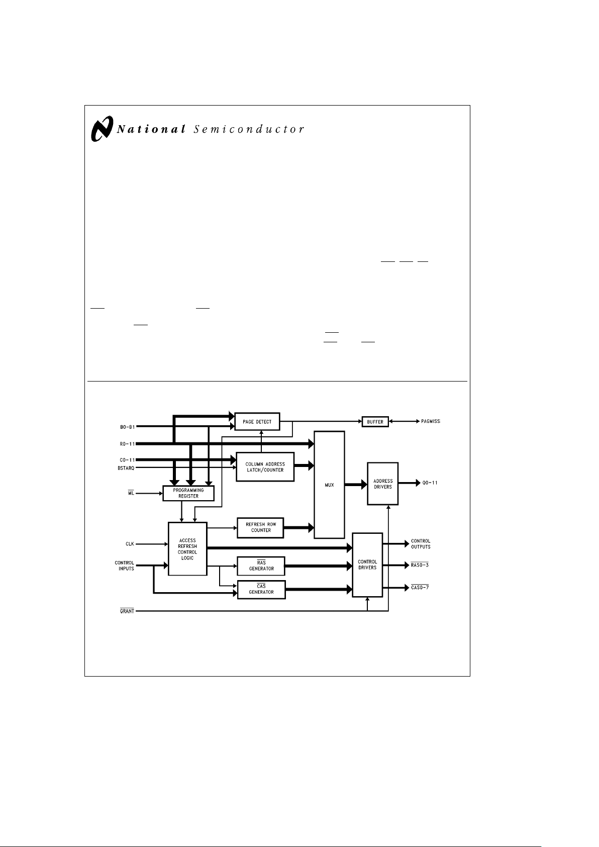
Block Diagram
TL/F/11718– 1
FIGURE 1
TRI-STATEÉis a registered trademark of National Semiconductor Corporation.
C
1995 National Semiconductor Corporation RRD-B30M75/Printed in U. S. A.
Page 2

DRAM Maximum Clock Package Bus Width Largest DRAM
Controller Frequency Type Supporting Possible
DP8440V-40 40 MHz 84-Pin PLCC 8, 16, 32 16 Mbits
DP8440VLJ-40 40 MHz 100-Pin PQFP 8, 16, 32 16 Mbits
DP8440VLJ-25 25 MHz 100-Pin PQFP 8, 16, 32 16 Mbits
DP8441VLJ-40 40 MHz 100-Pin PQFP 8, 16, 32, 64 64 Mbits
DP8441VLJ-25 25 MHz 100-Pin PQFP 8, 16, 32, 64 64 Mbits
Table of Contents
1.0 CONNECTION DIAGRAMS
2.0 FUNCTIONAL INTRODUCTION
3.0 SIGNAL DESCRIPTION
3.1 Address and Control Signals
3.2 DRAM Control Signals
3.3 Refresh Signals
3.4 Reset and Programming Signals
3.5 Clock Inputs
3.6 Power Signals and Capacitor Input
4.0 PROGRAMMING AND RESETTING
4.1 Reset
4.2 Programming Sequence
4.3 Programming Selection Bits
5.0 ACCESS MODES
5.1 Opening Access
5.2 Normal Mode
5.3 Page Mode
5.4 Burst Access
5.5 Inner Page Burst Access
6.0 REFRESH MODES
6.1 Auto-Internal Refresh
6.2 Externally Controlled Refresh
6.3 Error Scrubbing during Refresh
6.4 Extending Refresh
6.5 Refresh Types
7.0 WAIT SUPPORT
7.1 DTACK
During Opening Access
7.2 DTACK
During Page Access
7.3 DTACK
During Burst Access
7.4 Next Address or Early DTACK
Support
8.0 ABSOLUTE MAXIMUM RATINGS
9.0 DC ELECTRICAL CHARACTERISTICS
10.0 LOAD CAPACITANCE
11.0 AC TIMING PARAMETERS
12.0 AC TIMING WAVEFORMS
CLK and DECLK Timing
Refresh Timing
Refresh and Access Timing
Programming and Initialization Period Timing
Normal Mode Access Timing
Page Mode Access Timing
Burst Mode Access Timing
13.0 ERRATA
14.0 PHYSICAL DIMENSIONS
2
Page 3
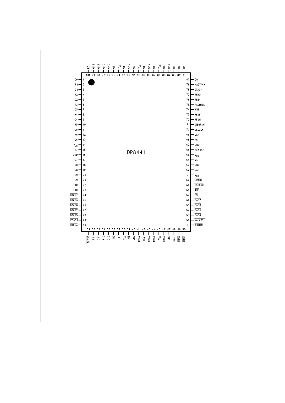
1.0 Connection Diagrams
TL/F/11718– 2
Top View
FIGURE 2
Order Number DP8441VLJ-40 (40 MHz Operation), DP8441VLJ-25 (25 MHz Operation)
See NS Package Number VLJ100A
3
Page 4
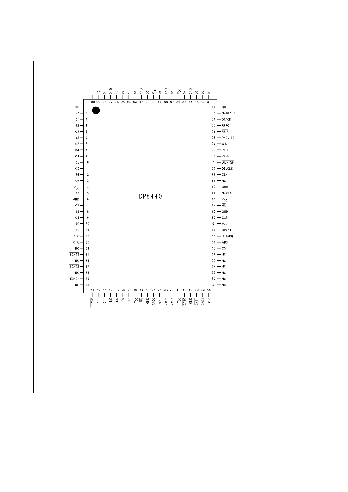
1.0 Connection Diagrams (Continued)
TL/F/11718– 38
Top View
FIGURE 3
Order Number DP8440VLJ-40 (40 MHz Operation), DP8440VLJ-25 (25 MHz Operation)
See NS Package Number VLJ100A
4
Page 5
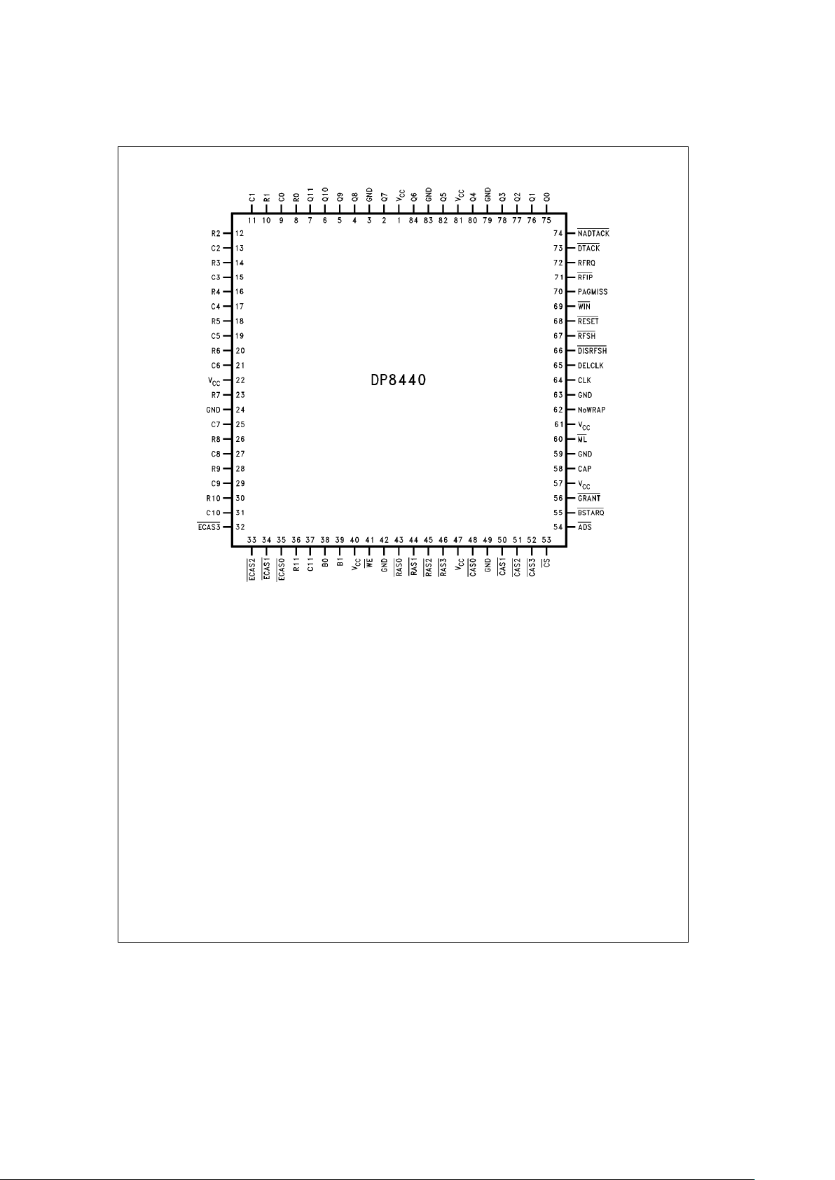
1.0 Connection Diagrams (Continued)
TL/F/11718– 3
Top View
FIGURE 4
Order Number DP8440V-40 (40 MHz Operation)
See NS Package Number V84A
5
Page 6

2.0 Functional Introduction
Reset and Programming: After the power up, the
DP8440/41 must be reset and programmed before it can be
used to access the DRAM. The chip is programmed through
the address bus.
Initialization Period: After programming, the DP8440/41
enter a 60 ms initialization period. During this time the
DP8440/41 perform refreshes to the DRAM. Further warm
up cycles are unnecessary. The user must wait until the
initialization is over to access the memory.
Modes of Operation: The DP8440/41 are synchronous
DRAM controllers. Every access is synchronized to the system clock. The controllers can be programmed in Page
Mode or Normal Mode. Burst accesses are dynamically requested through the input BSTARQ.
Opening Access: They involve a new row address. Regardless of the access mode programmed, opening accesses
behave in the same way. ADS
and CS initiate and qualify
every access. After asserting the ADS
, the DP8440/41 will
assert RAS
from the next rising edge of the CLK. The
DP8440/41 will hold the row address on the DRAM address
bus and guarantee that the row address is held for the Row
Address Hold Time (t
RAH
) programmed. The DRAM controller will then switch the internal multiplexor to place the column address on the DRAM address bus and assert CAS
.
DTACK
will wait the programmed number of wait states be-
fore asserting to indicate the end of the access.
Normal Access: If the controller is programmed in Normal
Mode (B1
e
1), RAS will assert and negate after the pro-
grammed RAS
low time. The user can perform burst access
if desired.
Page Access: The DP8440/41 have an internal page comparator. This feature enables the user to do a series of accesses without negating RAS
for as long as the row address
remains unchanged. The user needs to provide a new address for every access. The page comparator can also be
programmed as an input. This is beneficial for CPUs that
have an internal page comparator. The user can do burst
accesses while in page if desired.
Burst Access: These controllers can also generate new
addresses to burst a specific number of locations. The user
can choose to burst in a wrap around fashion for 2, 4, 8, 16
locations. Or, if the input NoWRAP is asserted, the controller will burst consecutive locations and the column address
will not wrap around. The controller must be programmed in
Latch Mode to generate the burst addresses.
Refresh Modes: The DP8440/41 can perform Automatic
Internal Refreshes, or Externally Controlled Refreshes. During a long page access the controller can queue up to six
refresh requests and burst refresh the addresses missed
when the access finishes.
Refresh Types: The DP8440/41 can be programmed to do
all RAS
Refresh, Staggered Refresh, Error Scrubbing during
Refresh or CAS
-before-RAS refresh.
Wait Support: These controllers provide wait logic for all
three types of accesses. The user needs to program the
desired number of wait states for opening, page and burst
accesses.
RAS
and CAS Configurations: The RAS outputs can be
programmed to drive one, two or four banks of memory and
the CAS
drivers can be programmed for byte writing in bus-
es up to 64 bits wide.
TRI-STATE Outputs and Multiporting: The GRANT
input
can be used for multi-porting. When high this input will
TRI-STATE the outputs, allowing another controller to drive
the DRAM.
Other Features: Independent RAS
precharge counters allow memory interleaving, thus back to back access to different memory banks is not delayed due to precharge.
The output NADTACK
can be used to pipeline one address,
getting the next access to start one clock early.
The input NoWRAP will increment the address during a
burst access in a linear fashion. This is convenient for
graphics or long page access.
Terminology: This paragraph explains the terminology
used in this data sheet. The terms negated and asserted are
used. For example, ECAS0
asserted means the ECAS0 input is at logic 0. The term NoWRAP asserted means that
NoWRAP is at logic 1.
6
Page 7
3.0 Signal Descriptions
3.1 ADDRESS AND CONTROL SIGNALS
Pin Device (if not Input/
Description
Name Applicable to All) Output
R0–11 DP8440 I ROW ADDRESS: These inputs are used to specify the row address during an access to
the DRAM. They are also used to program the chip when ML
is asserted.
R0–12 DP8441
C0–11 DP8440 I COLUMN ADDRESS: These inputs are used to specify the column address during an
access to the DRAM. They are also used to program the chip when ML
is asserted.
C0–12 DP8441
B0–B1 I BANK SELECT: Depending on programming, these inputs are used to select group RAS
and CAS outputs to assert during an access. They are also used to program the chip when
the ML
is asserted.
ECAS0–3 DP8440 I ENABLE CAS: These inputs asserted enable a single or group of CAS outputs. In
combination with the B0, B1 and the programming selection, these inputs select which
ECAS
0–7 DP8441
CAS
outputs will assert during an access. The ECAS signals can also be used to toggle a
group of CAS
outputs during page or burst mode accesses. They are also used to program
the chip when ML is asserted.
NoWRAP I NO WRAP: Asserting this signal causes the column address to be incremented
sequentially by one. The column address will not wrap around if NoWRAP is asserted.
(EXTNDRF)
When RFIP
is asserted, this signal is an EXTNDRF, used to extend refresh by any number
of CLK periods until EXTNDRF is negated.
NoLATCH DP8441 I COLUMN ADDRESS LATCH DISABLE: This input will disable ADS from latching the
column address when Latch Mode is selected.
ADS I ADDRESS STROBE: This input starts every access. Depending on programming this input
could latch the column address from the rising edge.
CS I CHIP SELECT: This input signal must be asserted to enable ADS to start an access.
DTACK O DATA TRANSFER ACKNOWLEDGE: This output can be programmed to insert wait
states into a CPU access cycle. DTACK
negated signifies a wait condition, when asserted
signifies that the access has taken place. This signal can be delayed a number of positive
or negative edges of clock. During burst accesses, DTACK
transitions increment the
column address.
NADTACK O NEXT ADDRESS or EARLY DTACK: This output asserts one clock cycle before DTACK.
This output can be used to request the next address in a sort of pipelining fashion or it
provides more time when DTACK
needs to be generated externally.
WAITIN DP8441 I WAIT INPUT: This input asserted delays DTACK for one extra clock period.
GRANT I MEMORY ACCESS GRANT: The GRANT input functions as an output enable. If negated,
it forces the outputs to a TRI-STATE condition.
PAGMISS I/O PAGE MISS: When programmed as an output, this signal asserts when either the row or
the bank address changes from the previous access cycle or the column address has
been incremented beyond the page boundary. If this pin is programmed as an input, it is
the responsibility of the system to tell the controller if the next access is within the page.
Useful for CPUs with internal page comparators, PAGMISS is valid only if ADS
and CS are
asserted.
BSTARQ/IBURST ACCESS REQUEST: This input enables the Burst Access Mode. This input can be
programmed to be active high or active low.
BSTARQ
7
Page 8
3.0 Signal Descriptions (Continued)
3.2 DRAM CONTROL SIGNALS
Pin Device (if not Input/
Description
Name Applicable to All) Output
Q0–11 DP8440 O DRAM ADDRESS: These output signals are the multiplexed outputs of the R0 – 11/12 and
C0–11/12 and form the DRAM address bus. These outputs contain the refresh address
Q0–12 DP8441
whenever RFIP
is asserted. They have high capacitive drivers with 20Xs series damping
resistors.
RAS0–3 O ROW ADDRESS STROBES: These outputs are asserted to latch the row address
contained on the outputs Q0–11/12 into the DRAM. When RFIP
is asserted, the RAS
outputs are used to latch the refresh row address contained on the Q0–11/12 outputs into
the DRAM. These outputs have high capacitive drivers with 20X series damping resistors.
CAS0–3 DP8440 O COLUMN ADDRESS STROBES: These outputs are asserted to latch the column address
contained on the outputs Q0–11/12 into the DRAM. When RFIP
is asserted and CAS-
CAS
0–7 DP8441
before-RAS
refresh is selected, the CAS outputs will assert 1T (one clock period) before
the RAS
outputs are asserted. These outputs have high capacitive drivers with 20X series
damping resistors.
WE O WRITE ENABLE: This output asserted specifies a write operation to the DRAM. When
negated, this output specifies a read operation to the DRAM. This output has a high
capacitive driver and a 20X series damping resistor.
WIN I WRITE ENABLE IN: This input is used to signify a write operation to the DRAM. The WE
output will follow this input. Also, this input controls the precharge time for Read and Write
during Burst Mode Access.
3.3 REFRESH SIGNALS
Pin Device (if not Input/
Description
Name Applicable to All) Output
RFRQ O REFRESH REQUEST: When RFRQ is asserted, it specifies that 15 msor120ms have
passed. If DISRFSH
is negated and the controller is not into an access cycle, the
DP8440/41 will perform an internal refresh. If DISRFSH
is asserted, RFRQ can be used to
externally request a refresh by asserting the input RFSH
.
RFIP O REFRESH IN PROGRESS: This output is asserted prior to a refresh cycle and is negated
when all the RAS
outputs are negated for that refresh.
RFSH I REFRESH: This input asserted with DISRFSH already asserted will request a refresh. If
this input is continually asserted, the DP8440/41 will perform refresh cycles in a burst
refresh fashion until the input is negated. If RFSH
is asserted with DISRFSH negated, the
internal refresh address counter is cleared. This technique is useful for burst refreshes.
DISRFSH I DISABLE REFRESH: This input is used to disable internal refreshes and must be asserted
when using RFSH for externally requested refreshes.
3.4 RESET AND PROGRAMMING SIGNALS
Pin Device (if not Input/
Description
Name Applicable to All) Output
ML I MODE LOAD: This input signal, when low, enables the internal programming register that
stores the programming information.
RESET I SYSTEM RESET: Reset forces the DP8440/41 to be set at a known state. VCC, CLK and
DELCLK have to reach their proper DC and AC specifications for at least 1 ms before
negating the RESET signal. All outputs are negated when RESET is asserted.
8
Page 9
3.0 Signal Descriptions (Continued)
3.5 CLOCK INPUTS
Pin Device (if not Input/
Description
Name Applicable to All) Output
CLK I SYSTEM CLOCK: This input may be in the range of 500 kHz to 40 MHz. This input is
generally a constant frequency but it may be controlled externally to change frequencies
for some arbitrary reason. This input provides the clock to the internal state machine that
arbitrates between accesses and refreshes. This clock’s positive edges and negative
edges are used to extend the DTACK
signal. This clock is also used as a reference for the
RAS precharge time, the RAS low during refresh time and CAS precharge time.
DELCLK I DELAY LINE CLOCK: The clock input DELCLK, may be in the range of 10 MHz to 40 MHz
and should be a multiple of 2 to have the DP8440/41 switching characteristics hold. If
DELCLK is not one of the above frequencies, the accuracy of the internal delay line will
suffer. This happens because the phase lock loop that generates the delay line assumes
an input clock frequency multiple of 2 MHz.
For example, if DELCLK input is 17 MHz and we choose to divide by 8 (program bits
C0–3), this will produce 2.125 MHz which is 6.25% off of 2 MHz. Therefore, the
DP8440/41 delay line will produce delays that are shorter (faster delays) than intended. If
divide by 9 was chosen, the delay line would produce longer delays (slower delays) than
intended (1.89 MHz instead of 2 MHz). This clock is also divided to create the internal
refresh clock.
3.6 POWER SIGNALS AND CAPACITOR INPUT
Pin Device (if not Input/
Description
Name Applicable to All) Output
V
CC
I POWER: Supply Voltage.
GND I GROUND: Supply Voltage Reference.
CAP I CAPACITOR: This input is used by the internal PLL for stabilization. The value of the
ceramic capacitor should be 0.1 mF and it should be connected between this input and
ground.
9
Page 10
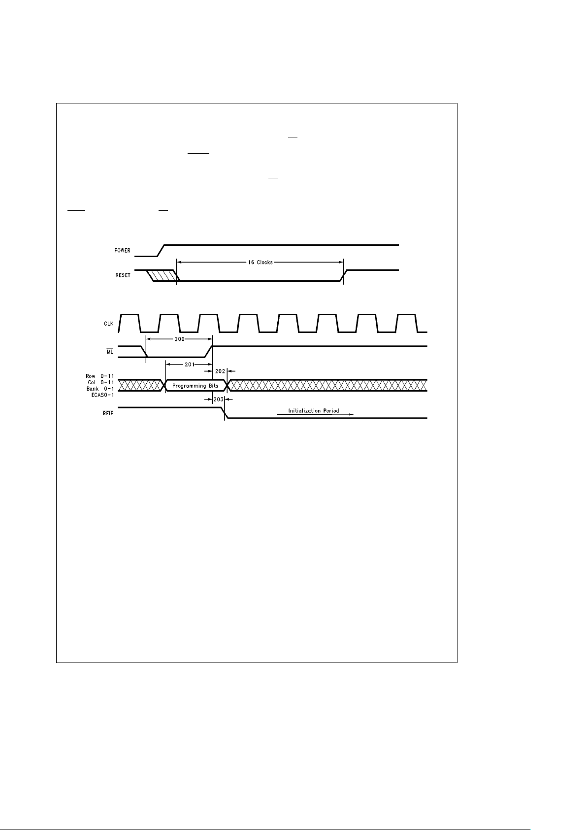
4.0 Programming and Resetting
4.1 RESET
After power up, the DP8440/41 must be reset and programmed before it can be used to access the DRAM. Reset
is accomplished by asserting the input RESET
for at least
16 positive edges of CLK after V
CC
stabilizes. After reset,
the part can be programmed.
4.2 PROGRAMMING
Programming is accomplished by presenting a valid programming selection on the row, column, bank selects and
ECAS
inputs and toggling the ML input from low to high.
When ML
goes high the part is programmed. After the first
programming after a reset the part will enter a 60 ms initialization period. During this period the controller will refresh
the memory, so further DRAM warm up cycles are not necessary. The user can program the part on the fly by pulsing
ML
low and high (provided that no refresh is in progress)
while a valid programming selection is on the address bus.
The part will not enter the initialization period when it is only
re-programmed.
TL/F/11718– 4
FIGURE 5. Reset
TL/F/11718– 5
FIGURE 6. Programming
10
Page 11
Programming the DP8440/41
4.3 PROGRAMMING SELECTION
RAS LOW AND PRECHARGE TIME
R1 R0
002T
013T
104T
115T
DTACK DURING OPENING ACCESS WILL ASSERT AFTER RAS
R3 R2
001T
012T
103T
114T
DTACK DURING BURST ACCESS WILL ASSERT AFTER CAS
R5 R4
000T
011T
102T
113T
DTACK DURING PAGE ACCESS WILL ASSERT AFTER CAS
R7 R6
000T
011T
102T
113T
PAGE SIZE SELECT
R9 R8
0 0 512
0 1 1024
1 0 2048
1 1 4096
WRAP AROUND SIZE
R11 R10
00 2
01 4
10 8
1116
11
Page 12
Programming the DP8440/41 (Continued)
4.3 PROGRAMMING SELECTION (Continued)
DIVISOR SELECT
C3 C2 C1 C0
000020
000119
001018
001117
010016
010115
011014
011113
100012
100111
101010
10119
11008
11017
11106
11115
RAS AND CAS CONFIGURATIONS AND REFRESH BEHAVIOR
C5 C4
0 0 All RAS
and all CAS are selected. B0 and B1 are not used. All RAS refresh.
0 1 If C6e0 Non Error B1 B0 is not Used If C6e1 Error B1 B0 is Not Used
Scrubbing Selected. All
0 RAS0 – 1
Scrubbing Selected.
0 RAS0 – 1 and CAS0 – 1, CAS4–5
CAS Selected. 2-Step
1 RAS2 – 3
All RAS Refresh.
1 RAS2 – 3 and CAS2 – 3, CAS6–7
Staggered Refresh. CAS Pairs Selected.
1 0 If C6e0 Non Error B1 B0 If C6e1 Error B1 B0
Scrubbing Selected.
0 0 RAS0
Scrubbing Selected.
0 0 RAS0, CAS0 –4
All CASs Selected.
0 1 RAS1
All RAS Refresh.
0 1 RAS1, CAS1 –5
4-Step Staggered
1 0 RAS2
CAS Pairs
1 0 RAS2, CAS2 –6
Refresh.
1 1 RAS3
Selected.
1 1 RAS3, CAS3 –7
1 1 If C6e0 Non Error B1 B0 is not used. If C6e1 Error B1 B0 is not used.
Scrubbing. 2-Step
0 RAS0 – 1 and CAS0,1,4,5
Scrubbing Selected.
0 RAS0 – 1 and CAS0,1,4,5
Staggered Refresh.
1 RAS2 – 3 and CAS2,3,6,7
All RAS Refresh.
1 RAS2 – 3 and CAS2,3,6,7
CAS Pairs Selected. CAS Pairs Selected.
ERROR SCRUBBING MODE SELECT
C6
0 Staggered Refresh (Non Error Scrubbing)
1 Error Scrubbing (No CAS
-before-RAS and No Staggered Refresh)
12
Page 13
Programming the DP8440/41 (Continued)
4.3 PROGRAMMING SELECTION (Continued)
ROW ADDRESS HOLD TIME SELECT t
RAH
C7
010ns
115ns
PAGMISS INPUT OR OUTPUT SELECT
C8
0 Input
1 Output
CAS PRECHARGE DURING BURST
C9 Read Cycle Write Cycle
0 (/2T1T
11T 2T
REFRESH MODE SELECT
C10
0 RAS
Only Refresh
1 CAS
-before-RAS Refresh
FINE TUNE REFRESH CYCLE
C11
015ms
1 120 ms
COLUMN ADDRESS COUNTER CONTROL SELECT
B0
0 DTACK
Falling Edge
1 DTACK
Rising Edge
PAGE OR NORMAL MODE SELECT
B1
0 Page Mode
1 Normal Mode
ADDRESS LATCH MODE
ECAS 0
0 Latch Mode
1 Fall Through Mode
BURST REQUEST SELECT (BSTARQ INPUT)
ECAS1
0 Active Low
1 Active High
CAS AND DTACK CLOCK EDGE SELECT
ECAS2
0 Rising Edge
1 Falling Edge
RESERVED
ECAS3
0
1
13
Page 14
5.0 Accessing Modes
The DP8440/41 are synchronous machines. They allow the
user to access the DRAM in three different ways, Page,
Burst and Normal mode. Every one of these accesses starts
in the same way, this datasheet calls it an Opening Access.
5.1 OPENING ACCESS
Every access starts with ADS
and CS asserting. ADS,CS
and the address inputs must meet setup timings with respect to the next rising edge of CLK. The DP8440/41
places the row address on the Q outputs and RAS
asserts
from the rising edge of CLK that ADS
is set up to. The
DP8440/41 guarantees the programmed Row Address Hold
Time, t
RAH
, before switching the internal multiplexer to
place the column address on the Q outputs. After the column address is valid on the Q outputs, the controller asserts
CAS
. The DRAM controller always guarantees t
ASC
of 0 ns.
DTACK
asserts after RAS according to the programming
selection (R2 –3). If the user programs Latch Mode, through
programming bit ECAS0
, the DRAM controller latches the
column address on the rising edge of ADS
(Normal or Page
Mode). If not, the controller keeps the latches in a fall
through mode.
5.2 NORMAL MODE
When the controller is programmed in Normal Mode
(B1
e
1), RAS asserts only for the programmed number of
clocks selected by R0 – 1, RAS
Low Time, and automatically
negates from a rising clock edge. To finish the access, CAS
negates from the same clock edge at which DTACK negates. After RAS
negates, the DP8440/41 will guarantee
the programmed number of positive edges of clock for RAS
precharge. RAS will not assert for another access until precharge is met.
Figure 7
shows an opening access (Normal
Mode) followed by a delayed access due to precharge (accessing the same bank). The second access is delayed by
one clock period to meet precharge time requirements.
TL/F/11718– 6
FIGURE 7. A Normal Opening Access and Delayed Access
(RAS
Low Time is Programmed for 2 Clocks)
14
Page 15

5.0 Accessing Modes (Continued)
5.3 PAGE MODE ACCESS
When the DP8440/41 is programmed for Page Accesses,
every access after the opening access needs a new address and a new ADS
. During Page Mode the DRAM con-
troller keeps RAS
asserted until there is a page miss detect-
ed. When a new access is requested, CAS
asserts from
the rising CLK edge that ADS
is set up to for reads, and
is delayed 1 clock for writes. DTACK
asserts according to
the programming selection in bits R6–7. At the end of a
page access only CAS
and DTACK negate and they negate
on the same clock edge.
During page accesses only CAS
and DTACK toggle until
there is a page miss. When a page miss is detected, the
DP8440/41 will negate RAS
and meet the programmed precharge time. CPUs with page comparators can program the
DRAM controller’s page comparator as an input. When this
input asserts, it indicates that a page change has occurred,
RAS
will negate and the controller will meet the precharge
time.
Figure 8
shows an opening access followed by two
page accesses. The first page access is a ‘‘page hit,’’ the
second access is out of page.
TL/F/11718– 7
FIGURE 8. Opening Access Followed by Page Accesses
15
Page 16

5.0 Accessing Modes (Continued)
TL/F/11718– 39
FIGURE 9. Page ‘‘Hit’’ Write and Read Followed by Page Miss
(CAS
Assertion for Write is Delayed One Clock)
16
Page 17

5.0 Accessing Modes (Continued)
5.4 BURST ACCESS
The DP8440/41 can also perform burst accesses to several
locations in different wrap around sizes. The user requests
burst accesses by asserting the input BSTARQ. BSTARQ
must be negated before the last DTACK
. This input can be
programmed to be active high or active low. The number of
burst locations can be programmable to be modulo 2, 4, 8,
or 16. If the beginning of the sequence does not start with 0,
00, 000 or 0000, the controller will wrap around. The user
may choose not to wrap by asserting the input NoWRAP, in
this case the controller will increment the column address
linearly. A NoWRAP burst access cannot cross a page
boundary unless the port is programmed in Page Mode,
in which case a Page Miss occurs and the burst access
terminates. Burst accesses can be requested at any time.
The user can do burst accesses while in Page Mode (see
Inner Page Burst), or in Normal Mode. The column address
is incremented by DTACK
transitions as programmed by B0.
Thus, if DTACK
is programmed as 0 T, the column address
will not be incremented and the CPU must provide the addresses to burst. CAS
and DTACK can be programmed to
toggle from either clock edge. The CAS
precharge time is
programmable to 1 or (/2 clocks during read accesses and 1
or 2 clocks during write accesses ((/2T
e
10 ns minimum of
CAS
precharge).
TL/F/11718– 40
FIGURE 10. Burst Write Access
Programming Selection Bits Mode
DTACK during Opening R3e1, R2e03T
DTACK during Burst R5e1, R4e02T
CAS Precharge during Burst C9e0 Read: (/2T, Write: 1T
Column Address Counter Control BOe1 DTACK Rising Edge
CAS and DTACK Edge Select ECAS2e0 Rising Edge
FIGURE 11. Burst Write Access
17
Page 18

5.0 Accessing Modes (Continued)
TL/F/11718– 41
FIGURE 12. Burst Read Access
Programming Selection Bits Mode
DTACK during Opening R3e1, R2e03T
DTACK during Burst R5e1, R4e02T
CAS Precharge during Burst C9e0 Read: (/2T, Write: 1T
Column Address Counter Control BOe0 DTACK Falling Edge
CAS and DTACK Edge Select ECAS2e0 Falling Edge
18
Page 19

5.0 Accessing Modes (Continued)
5.5 INNER PAGE BURST ACCESS
If the user plans to burst within page access, the
DP8440/41 must be programmed in Latch Mode. In this
case, the DRAM latches the column address on the rising
edge of ADS
. When the controller detects BSTARQ assert-
ed, DTACK
transitions will increment the column address in
modulo 2, 4, 8, or 16 with wrap around at the boundaries for
as long as BSTARQ is asserted. If the user asserts the input
NoWRAP, the controller increments the address sequentially. After an InnerPage Burst, RAS
will stay asserted until
there is a page miss detected.
Figure 13
shows an opening
access followed by a page access, two burst accesses and
a new access in a different page (page miss).
TL/F/11718– 9
FIGURE 13. Opening Access followed by a Page ‘‘HIT’’ Access with 2 Bursts
19
Page 20

6.0 Refresh Modes
The DP8440/41 support auto-internal refresh, and externally control refresh. The DP8440/41 arbitrates between refreshes and accesses and guarantees precharge timings after every access and refresh. The DRAM controller will never interrupt an access in progress to do a refresh, nor will it
interrupt a refresh in progress when an access is requested.
After every refresh the DRAM controller will guarantee the
programmed precharge time before RAS
can assert for a
new access or for a second refresh. The refresh period can
be programmed for 15 ms or for 120 ms.
6.1 AUTO-INTERNAL REFRESH
This refresh scheme is completely transparent to the CPU.
The DP8440/41 will refresh the DRAM every 15 msor
120 ms, depending on the programming selection. When the
refresh counter expires (every 15 ms or 120 ms) the RFRQ
output asserts. On the next rising edge of clock RFIP
as-
serts and, one clock period later, RAS
s assert. RFIP ne-
gates on the same clock edge that RAS
s negate. If the user
is doing long page or burst accesses, the DP8440/41 will
keep track of up to 6 missed refreshes. At the end of the
access the DRAM controller will burst refresh the locations
missed during the access.
TL/F/11718– 10
FIGURE 14. Autointernal Refresh (2T of RAS Low and Precharge)
20
Page 21

6.0 Refresh Modes (Continued)
6.2 EXTERNALLY CONTROLLED REFRESH
The user can perform externally controlled refreshes by asserting the DISRFSH
and RFSH input signals. When these
inputs assert, the DP8440/41 will perform a refresh as soon
as possible. If the user keeps RFSH
asserted with DISRFSH
already asserted, the DRAM controller will burst refresh the
memory for as long as the inputs are valid. The controller
will guarantee the RAS
low and RAS precharge times for
every refresh. The user can choose to monitor the output
RFRQ to externally request a refresh. When RFRQ asserts,
it indicates that the refresh counter has expired.
TL/F/11718– 11
FIGURE 15. Externally Controlled Refresh (2T of RAS Low and Precharge)
21
Page 22

6.0 Refresh Modes (Continued)
6.3 ERROR SCRUBBING DURING REFRESH
The DP8440/41 supports error scrubbing during all RAS
DRAM refreshes. Error scrubbing during refresh is selected
through bits C4–C6 with bit C6 set during programming. Error scrubbing can not be used with staggered refresh. Error
scrubbing during refresh allows a CAS
or group of CASsto
assert during the all RAS
refresh as shown in
Figure 16
.
This allows data to be read from the DRAM array and
passed through an Error Detection And Correction Chip,
EDAC. If the EDAC determines that the data contains a single bit error and corrects that error, the refresh cycle can be
extended with the input extend refresh, EXTNDRF, and a
read-modify-write operation can be performed by asserting
WE
. It is the responsibility of the designer to ensure that WE
is negated. The DP8440 has a 26-bit internal refresh address counter that contains the 12 row, 12 column and 2
bank addresses. The DP8441 has a 28-bit internal refresh
address counter that contains the 13 row, 13 column and 2
bank addresses. These counters are configured as bank,
column, row with the row address as the least significant
bits. The bank counter bits are then used with the programming selection to determine which CAS
or group of CASs
will assert during a refresh.
TL/F/11718– 42
FIGURE 16. Error Scrubbing during Refresh (Two Refresh Cycles Shown)
22
Page 23

6.0 Refresh Modes (Continued)
6.4 EXTENDING REFRESH
The programmed number of periods of CLK that refresh
RAS
s are asserted can be extended by one or multiple peri-
ods of CLK. Only the all RAS
(with or without error scrubbing) type of refresh can be extended. To extend a refresh
cycle, the input extend refresh, EXTNDRF, must be asserted before the positive edge of CLK that would have negated
all the RAS
outputs during the re fresh cycle and after the
positive edge of CLK which starts all RAS
outputs during the
refresh as shown in
Figure 17
. This will extend the refresh to
the next positive edge of CLK and EXTNDRF will be sampled again. The refresh cycle will continue until EXTNDRF is
sampled low on a positive edge of CLK.
TL/F/11718– 43
FIGURE 17. Extending Refresh with the Extend Refresh (EXTNDRF) Input
23
Page 24

6.0 Refresh Modes (Continued)
6.5 REFRESH TYPES
The DP8440/41 support RAS
Only refresh and CAS-before-
RAS
refresh. RAS only refresh can be programmed to be
staggered or non-staggered. Staggered refresh reduces
peak current requirements and system noise.
The DP8440/41 have a large enough refresh address counter for error scrubbing during refresh. If error scrubbing is
desired, the user must select the All RAS
refresh option.
TL/F/11718– 12
FIGURE 18. All RAS Refresh with 2Ts of RAS Low and Precharge.
All RAS
refresh must be programmed when doing Error Scrubbing.
TL/F/11718– 13
FIGURE 19. Staggered Refresh with 2Ts RAS low and Precharge.
Staggered refresh is good for noise sensitive systems.
Clearing the Refresh Counter and Refresh Clock: The
user can clear the refresh counter by pulsing RFSH
low for
two clocks while DISRFSH
is negated. If RFSH is kept as-
serted for 500 ns, the refresh clock will also be cleared.
TL/F/11718– 34
24
Page 25

7.0 Wait Support
The DP8440/41 provide full wait support for all types of
accesses. Through the DTACK
output, the user can insert
wait states to provide the necessary time for completing a
memory access. The user needs to program how DTACK
will assert during Opening, Page or Burst accesses. The
user can program DTACK
to assert from the rising edge of
clock or from the falling edge of clock.
7.1 OPENING ACCESS
Figures 20
and21show DTACK during opening accesses.
DTACK
asserts for only one clock cycle. CAS negates from
the same clock edge DTACK
negates. When programmed
in Normal Mode, RAS
will negate after the programmed
RAS
low time. When programmed in Page Mode, RAS will
stay asserted until there is a page miss.
TL/F/11718– 14
FIGURE 20. DTACK Programmed to Assert from a Positive Edge of Clock
TL/F/11718– 15
FIGURE 21. DTACK Programmed to Assert from a Negative Edge of Clock
25
Page 26

7.0 Wait Support (Continued)
7.2 PAGE ACCESSES
During page accesses, DTACK
(and CAS) will assert from
either clock edge according to programming bit ECAS2
.
Figure 22
shows different DTACK assertions during page
accesses, they follow an opening access with 1 wait state.
DTACK
and CAS assert on the rising edge of clock.
TL/F/11718– 16
FIGURE 22a. DTACK is Programmed 1T for Openings and 0T during Page
TL/F/11718– 17
FIGURE 22b. DTACK is Programmed 1T for Openings and 1T during Page
TL/F/11718– 18
FIGURE 22c. DTACK is Programmed 1T for Openings and 2T during Page
TL/F/11718– 19
FIGURE 22d. DTACK is Programmed 1T for Openings and 3T during Page
Note: DTACK is programmed to assert from a positive clock edge.
26
Page 27

7.0 Wait Support (Continued)
7.3 BURST ACCESSES
During burst accesses, DTACK
will assert from the clock
edge chosen through programming bit ECAS2
. CAS automatically negates and the controller guarantees the minimum CAS
precharge time according to programming bit C9.
CAS
and DTACK can be programmed to assert from either
clock edge.
During burst accesses, the input BSTARQ must be asserted
for CAS
to toggle.
Figure 23
shows how DTACK asserts
during burst accesses, following an opening access with
one wait state. In
Figure 23a
, when the number of wait
states in a burst is programmed to zero, DTACK
remains
asserted throughout the burst. The address is not incremented by the DRAM controller. It is the responsibility of the
user to provide incrementing addresses.
For the controller to increment the column address DTACK
must toggle.
TL/F/11718– 20
FIGURE 23a. 1T during Opening and 0T during Burst. DTACK stays asserted during the burst.
TL/F/11718– 21
FIGURE 23b. 1T during Opening, 1T during Burst
TL/F/11718– 22
FIGURE 23c. 1T during Opening, 2T during Burst
TL/F/11718– 23
FIGURE 23d. 1T during Opening, 3T during Burst
27
Page 28

7.0 Wait Support (Continued)
7.4 NADTACK
During any accesses, this output asserts one clock period
before DTACK
asserts, except when DTACK is programmed for 1T in normal accesses or 0T during page or
burst accesses.
The user can use this output to request the next address in
a sort of pipelining fashion. This output can also be used to
generate a more accurate DTACK
for special applications.
The next figures show how NADTACK
asserts in different
cases.
TL/F/11718– 24
FIGURE 24a. DTACK is Programmed for 4Ts and to Assert from the Rising CLK Edge
TL/F/11718– 25
FIGURE 24b. DTACK is Programmed for 2Ts and to Assert from the Falling CLK Edge
TL/F/11718– 26
FIGURE 24c. DTACK and CAS assert from the rising edge of CLK. DTACK is programmed for 1T. NADTACK asserts
with DTACK
during the opening access. During Page Accesses, NADTACK asserts one clock before DTACK.
28
Page 29

8.0 Absolute Maximum Ratings
If Military/Aerospace specified devices are required,
please contact the National Semiconductor Sales
Office/Distributors for availability and specifications.
Temperature Under Bias 0
§
Ctoa70§C
Storage Temperature
b
65§Ctoa150§C
All Input and Output Voltage
with Respect to GND
b
0.5V toa7V
ESD Rating 2000V
Recommended Operating
Conditions
Supply Voltage, V
CC
4.75V to 5.25V
Operating Free Air Temperature 0§Ctoa70§C
9.0 DC Electrical Characteristics T
A
e
0§Ctoa70§C, V
CC
e
5Vg5%, GNDe0V
Symbol Parameter Conditions Min Typ Max Units
V
IH
Logical 1 Input Voltage Tested with a Limited
2.00 V
CC
a
0.5 V
Functional Pattern
V
IL
Logical 0 Input Voltage Tested with a Limited
b
0.5 0.8 V
Functional Pattern
V
OH1
Q and WE Outputs I
OH
eb
10 mA V
CC
b
1.0 V
V
OL1
Q and WE Outputs I
OL
e
10 mA 0.5 V
V
OH2
All Outputs Except Qs, WE I
OH
eb
5mA V
CC
b
1.0 V
V
OL2
All Outputs Except Qs, WE I
OL
e
5 mA 0.5 V
I
IN
Input Leakage Current V
IN
e
VCCor GND
b
10 10 mA
I
CC2
Supply Current CLK at 40 MHz (I/Os Active) 260 mA
C
IN
Input Capacitance fINat 1 MHz 5 10 pF
10.0 Load Capacitance
Q0–11 C
L
e
50 pF
WE C
L
e
50 pF
RAS0–3 C
L
e
50 pF
CAS0–3 C
L
e
50 pF (DP8440)
CAS
0–7 C
L
e
50 pF (DP8441)
Other outputs C
L
e
50 pF
Adder Table for Higher Capacitive Loads
Output ns/10 pF
Linear up to
Maximum Load
Q0–11 0.350 360 pF max
WE 0.548 500 pF max
RAS0–3 0.282 125 pF max
CAS0–3 0.282 125 pF max (DP8440)
CAS0–7 0.334 67 pF max (DP8441)
11.0 AC Timing Parameters
Two speed selections are given, the DP8440/41-40 and the
DP8440/41-25. The differences between the two parts are
the maximum operating frequencies of the input CLKs and
the maximum delay specifications. Low frequency applications may use the ‘‘-40’’ part to gain improved timing.
The AC timing parameters are grouped into sectional numbers as shown below. These numbers also refer to the timing diagrams.
1–6 Clock Parameters
50–53 TRI-STATE Parameters
100–109 Refresh Parameters
200–203 Programming Parameters
300–325 Common Parameters
400–423 Fast access parameters used in burst and Page
Mode accesses
29
Page 30

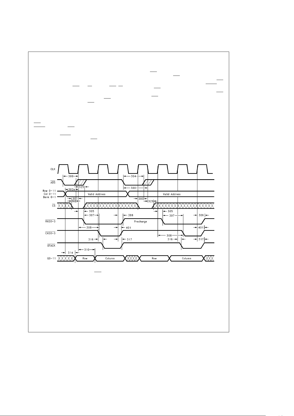
11.0 AC Timing Parameters (Continued)
Ý
Symbol Description
DP8440/41-40 DP8440/41-25
40 MHz Devices 25 MHz Devices
Min Max Min Max
CLOCK PARAMETER
1t
CLKP
Clock Period 25 40
2, 3 t
WCLK
Clock Pulse Width 10 15
4t
DCLKP
DELCLK Period 25 25
5, 6 t
WDCLK
DELCLK Pulse Width 10 10
TRI-STATE PARAMETER
50 t
PZL
TRI-STATE to Low Voltage Level 20 25
51 t
PZH
TRI-STATE to High Voltage Level 20 25
52 t
PLZ
Low Voltage Level to TRI-STATE 25 30
53 t
PHZ
High Voltage Level to TRI-STATE 25 30
REFRESH PARAMETER
100 t
SRFCK
RFSH Asserted Set up to CLK High 6 8
101 t
HRFCK
RFSH Asserted Hold Time 3 4
102 t
SDRFCK
DISRFSH Asserted Setup to CLK High 6 8
103 t
HDRFCK
DISRFSH Asserted Hold Time 3 4
104 t
PCKRFL
CLK High to RFIP Asserted 17 20
105 t
PCKRFH
CLK High to RFIP Negated 34 36
106 t
PCKRQL
CLK High to RFRQ Asserted 13 15
107 t
PCKRQH
CLK High to RFRQ Negated 12 14
108 t
PCKRFRASL
CLK High to RAS Asserted During Refresh 23 25
109 t
PCKRFRASH
CLK High to RAS Negated During Refresh 19 21
PROGRAMMING PARAMETER
200 t
WML
ML Pulse Width 15 15
201 t
SPBML
Programming Bits Setup to ML High 18 18
202 t
HPBML
Programming Bits Hold Time 6 6
203 t
PMLRFL
ML High to RFIP Asserted 18 18
30
Page 31

11.0 AC Timing Parameters (Continued)
Ý
Symbol Description
DP8440/41-40 DP8440/41-25
40 MHz Devices 25 MHz Devices
Min Max Min Max
COMMON PARAMETER
300 t
SADSCK
ADS Asserted Setup to CLK High 10 12
301 t
SCSCK
CS Asserted Setup to CLK High 10 12
302a t
SADDCK
Row, Column and Bank Address Valid Setup to CLK High 0 0
302b t
SADDCKP
Row and Bank Address Setup to CLK High in Page Mode Access 18 18
303 t
SCSADS
CS Asserted Setup to ADS Negated 6 7
304 t
WADS
ADS Pulse Width (Asserted) 6 6
305 t
PCKRASL
CLK High to RAS Asserted 17 19
306 t
PCKRASH
CLK High to RAS Negated 18 20
307a t
PRASCAS0
RAS Asserted to CAS Asserted (t
RAH
e
10 ns) 20 20
307b t
PRASCAS1
RAS Asserted to CAS Asserted (t
RAH
e
15 ns) 25 25
308a t
PCKCAS0
CLK High to Delay CAS Asserted (t
RAH
e
10 ns) 60 60
308b t
PCKCAS1
CLK High to Delay CAS Asserted (t
RAH
e
15 ns) 65 65
309a t
RAH0
Row Address Hold Time (t
RAH
e
10 ns) 10 10
309b t
RAH1
Row Address Hold Time (t
RAH
e
15 ns) 15 15
310a t
PCKCV0
CLK High to Column Address Valid (t
RAH
e
10 ns) 52 52
310b t
PCKCV1
CLK High to Column Address Valid (t
RAH
e
15 ns) 57 57
311 t
ASC
Column Address Setup Time (t
ASC
e
0 ns) 0 0
312 t
PECSCASL
ECAS Asserted to CAS Asserted 14 16
313 t
PECSCASH
ECAS Negated to CAS Negated 14 16
314 t
PAQ
Row, Column and Bank Address to Q Valid 17 18
315 t
PWINWE
WIN to WE Out 14 16
316 t
PCKDTL
CLK High to DATCK Asserted 15 17
317 t
PCKDTH
CLK High to DTACK Negated 15 17
318 t
PCKLDTL
CLK Low to DATCK Asserted 16 18
319 t
PCKLDTH
CLK Low to DTACK Negated 16 18
320 t
PCKNADL
CLK High to NADTACK Asserted 15 17
321 t
PCKNADH
CLK High to NADTACK Negated 15 17
322 t
PCKLNADL
CLK Low to NADTACK Asserted 15 17
323 t
PCKLNADH
CLK Low to NADTACK Negated 15 17
324a t
PRASCV0
RAS Asserted to Column Address Valid (t
RAH
e
10 ns) 38 38
324b t
PRASCV1
RAS Asserted to Column Address Valid (t
RAH
e
15 ns) 43 43
325 t
HCSCK
CS Asserted Hold from CLK High 3 4
31
Page 32

11.0 AC Timing Parameters (Continued)
Ý
Symbol Description
DP8440/41-40 DP8440/41-25
40 MHz Devices 25 MHz Devices
Min Max Min Max
FAST ACCESS PARAMETER
400 t
PCKCASL
CLK High to CAS Asserted 15.5 16
401 t
PCKCASH
CLK High to CAS Negated 17.5 18
402 t
PCKLCASL
CLK Low to CAS Asserted 18.5 19
403 t
PCKLCASH
CLK Low to CAS Negated 18.5 19
404 t
WCASPC
CAS Precharge when Programmed as (/2T during Burst 10 10
405 t
PCKCASB
CLK to CAS Asserted when Programmed as (/2T during Burst 17 35 17 36
406 t
PCKCVB
CLK to Column Address Valid when B0e1 during Programming 27 27
407 t
PCKCVLB
CLK to Column Address Valid when B0e0 during Programming 32 32
408 t
PCKPMH
CLK to PAGMISS Asserted During Burst and NoWRAP 14 14
409 t
SBARCK
BSTARQ Asserted Setup to CLK 10 10
410 t
HBARNCK
BSTARQ Asserted Hold from CLK (CLK following DTACK Negation) 16 17
411 t
SNWCK
NoWRAP Asserted Setup to CLK (NADTACK)56
412 t
HNWCK
NoWRAP Asserted Hold from CLK (DTACK)56
413 t
SNLADS
NoLATCH Asserted Setup to ADS 56
414 t
HNLCK
NoLATCH Asserted Hold from CLK 5 6
415 t
SPMCK
PAGMISS Input Asserted Setup to CLK 16 16
416 t
HPMCK
PAGMISS Input Asserted Hold from CLK 5 6
417 t
PADDPMH
Row and Bank Address Valid to PAGMISS Asserted 13 13
418 t
PCKPML
CLK High to PAGMISS Negated 17 17
419 t
SWICLK
WAITIN Asserted Setup to CLK (NADTACK)56
420 t
HWICLK
WAITIN Asserted Hold from CLK (NADTACK)56
421 t
SADSCKP
ADS Setup to CLK in Page Mode 22 22
422 t
PADSPMH
ADS to PAGMISS High in Page Mode 16 16
423 t
HADSCKP
ADS Hold from CLK before Assertion in Page Mode 4 4
424 t
SCSKP
CS Setup to CLK in Page Mode 22 22
12.0 AC Timing Waveforms: DP8440/41
TL/F/11718– 27
FIGURE 25. CLK and DELCLK Timing
Number
DP8440/41-40 DP8440/41-25
Min Max Min Max
125 40
210 15
310 15
425 25
510 10
610 10
32
Page 33

12.0 AC Timing Waveforms: DP8440/41 (Continued)
TL/F/11718– 28
FIGURE 26. Refresh Timing
DP8440/41-40
Number Min Max
100 6
101 3
102 6
103 3
104 17
105 34
106 13
107 12
305 17
306 18
400 15.5
401 17.5
DP8440/41-25
Number Min Max
100 8
101 4
102 8
103 4
104 20
105 36
106 15
107 14
305 19
306 19
400 16
401 18
33
Page 34

12.0 AC Timing Waveforms: DP8440/41 (Continued)
TL/F/11718– 29
FIGURE 27. Refresh and Access Timing
Number
DP8440/41-40 DP8440/41-25
Min Max Min Max
104 17 20
105 34 36
106 13 15
107 12 14
300 10 12
301 10 12
302a 0 0
302b 18 18
305 17 19
306 18 19
308a 60 60
308b 65 65
315 14 16
316 15 17
401 17.5 18
34
Page 35

12.0 AC Timing Waveforms: DP8440/41 (Continued)
TL/F/11718– 30
FIGURE 28. Programming and Initialization Period Timing
Number Min Max
200 15
201 18
202 6
203 18
35
Page 36

12.0 AC Timing Waveforms: DP8440/41 (Continued)
TL/F/11718– 31
FIGURE 29a. Normal Mode Access TimingÐDP8440/41-40
Number
DP8440/41-40
Min Max
300 10
301 10
302a 0
303 6
304 6
305 17
306 18
307a 20
307b 25
308a 60
Number
DP8440/41-40
Min Max
308b 65
309a 10
309b 15
310a 52
310b 57
311 0
312 14
313 14
314 17
315 14
Number
DP8440/41-40
Min Max
316 15
317 15
318 16
319 16
320 15
325 3
400 15.5
401 17.5
402 18.5
403 18.5
36
Page 37

12.0 AC Timing Waveforms: DP8440/41 (Continued)
TL/F/11718– 31
FIGURE 29b. Normal Mode Access TimingÐDP8440/41-25
Number
DP8440/41-25
Min Max
300 12
301 12
302a 0
303 7
304 6
305 19
306 19
307a 20
307b 25
308a 60
Number
DP8440/41-25
Min Max
308b 65
309a 10
309b 15
310a 52
310b 57
311 0
312 16
313 16
314 18
315 16
Number
DP8440/41-25
Min Max
316 17
317 17
318 18
319 18
320 17
325 4
400 16
401 18
402 19
403 19
37
Page 38

12.0 AC Timing Waveforms: DP8440/41 (Continued)
TL/F/11718– 32
FIGURE 30. Burst Mode Access Timing When Using Rising CLK Edge
Number
DP8440/41-40 DP8440/41-25
Min Max Min Max
300 10 12
301 10 12
302a 0 0
304 6 6
305 17 19
306 18 19
307a 20 20
307b 25 25
308a 60 60
308b 65 65
310a 52 52
310b 57 57
314 17 18
316 15 17
317 15 17
Number
DP8440/41-40 DP8440/41-25
Min Max Min Max
318 16 18
400 15.5 16
401 17.5 18
402 18.5 19
403 18.5 19
404 10 10
405 17 35 17 36
406 27 27
409 10 10
410 16 17
411 5 6
412 5 6
417 13 13
418 17 17
38
Page 39

12.0 AC Timing Waveforms: DP8440/41 (Continued)
TL/F/11718– 33
FIGURE 31a. Page Mode Access TimingÐDP8440/41-40
Number
DP8440/41-40
Min Max
302b 21
303 6
304 6
305 17
306 18
307a 20
307b 25
308a 60
308b 65
Number
DP8440/41-40
Min Max
310a 52
310b 57
314 17
316 15
317 15
400 15.5
401 17.5
407 32
408 14
413 5
Number
DP8440/41-40
Min Max
414 5
415 16
416 5
417 13
418 17
419 5
420 5
421 22
423 4
424 22
39
Page 40

12.0 AC Timing Waveforms: DP8440/41 (Continued)
TL/F/11718– 33
FIGURE 31b. Page Mode Access TimingÐDP8440/41-25
Number
DP8440/41-25
Min Max
302b 18
303 7
304 6
305 19
306 19
307a 20
307b 25
308a 60
308b 65
Number
DP8440/41-25
Min Max
310a 52
310b 57
314 18
316 17
317 17
400 16
401 18
407 32
408 14
413 6
Number
DP8440/41-25
Min Max
414 6
415 16
416 5
417 13
418 17
419 5
420 5
421 22
423 4
424 22
40
Page 41

12.0 AC Timing Waveforms: DP8440/41 (Continued)
TL/F/11718– 35
FIGURE 32. Burst Mode Access Timing When Using Falling CLK Edge (ECAS
2e1)
Number
DP8440/41-40 DP8440/41-25
Min Max Min Max
300 10 12
301 10 12
302b 21 18
304 6 6
305 17 19
306 18 19
307a 20 20
307b 25 25
308a 60 60
308b 65 65
310a 52 52
310b 57 57
314 17 18
316 15 17
317 15 17
Number
DP8440/41-40 DP8440/41-25
Min Max Min Max
318 16 18
400 15.5 16
401 17.5 18
402 18.5 19
403 18.5 19
404 10 10
405 17 35 17 36
407 32 32
409 10 10
410 16 17
411 5 6
412 5 6
417 13 13
418 17 17
419 5 6
41
Page 42

13.0 Errata for DP8440/41
ERRATUMÝ1
While programmed in Normal Mode, the RAS signals may
negate (/2 clock before the CAS
signals for the last burst
access. This can be a problem for write accesses, in which
the RAS
hold time may not be met for some DRAM arrays.
Recommended Fix
The RAS
assertion time can be extended (/2 clock by holding off the negation of the BSTARQ signal (Burst Access
Request) until after the falling edge of the last DTACK
.If
this approach is taken, then BSTARQ must then be negated
before the clock edge which negates the last DTACK
to
guarantee no other accesses take place.
TL/F/11718– 36
ERRATUMÝ2
The NoWrap signal and EXTNDRF signal are multiplexed
on the same pin. NoWrap is asserted when doing sequential
burst acceses that don’t wrap around. EXTNDRF (Extend
Refresh) is used to extend a refresh while it is occurring.
A problem arises when a NoWrap burst access occurs
slightly before or during a refresh cycle. The DP8440/41
goes into a refresh cycle, however, because the NoWrap/
EXTNDRF signal is asserted, the refresh cycle may last indefinitely and the access will never complete.
Recommended Fix
The designer must be reminded that NoWrap/EXTNDRF
are multiplexed and if NoWrap acceses are used in the design, it is recommended that the NoWrap be gated with the
RFIP
signal as outlined below.
TL/F/11718– 37
ERRATUMÝ3
The NoWrap signal and BSTARQ (Burst Request) signal
should not be asserted on the same clock edge. This is only
a problem when doing NoWrap burst accesses.
Recommended Fix
The NoWrap signal should be asserted from ONE clock after the BSTARQ signal is asserted. This will have no effect
on the operation of the burst access and will prevent any
problems from occurring.
ERRATUM
Ý
4
When using external refreshes, the start of an access may
be delayed slightly if the access occurs near the assertion
of the RFRQ (Refresh Request) signal.
Recommended Fix
There is no guarantee the access will begin immediately
after the assertion of ADS
, therefore, the internal timing sig-
nals, DTACK
or NADTACK, should always be used as a
reference to generate the acknowledge signal to the CPU.
Delayed Access due to RFRQ
TL/F/11718– 44
42
Page 43

13.0 Errata for DP8440/41 (Continued)
ERRATUM
Ý
5
When operating in Page Mode, an access cannot start on
the clock edge immediately following the negation of
DTACK
. If back-to-back accesses are done in this way, the
CAS
signals will remain low during a refresh as shown in the
timing diagram.
Recommended Fix
There should be at least one idle clock between the negation of DTACK
and the start of a new access.
Illegal Back-to-Back Accesses in Page Mode
TL/F/11718– 45
ERRATUMÝ6
When starting a page access, there is a hold time from the
rising edge of the clock when ADS
cannot assert. This hold
time (parameter 423 in the datasheet) is 4 ns and only applies when operating in Page Mode.
Recommended Fix
ADS
assertion should be delayed at least 4 ns from the
rising edge of the clock when in Page Mode operation.
Parameter 423: ADS
Hold Time before Assertion
TL/F/11718– 46
43
Page 44

13.0 Errata for DP8440/41 (Continued)
ERRATUM
Ý
7
Both CS and ADS are sampled asynchronously to the clock,
consequently there should be no overlap in their assertion
unless an access is being attempted.
Recommended Fix
Avoid asserting CS
and ADS simultaneously unless attempt-
ing a DRAM access.
Illegal Overlap of CS
and ADS
TL/F/11718– 47
44
Page 45

14.0 Physical Dimensions inches (millimeters)
Plastic Chip Carrier (PLCC)
Order Number DP8440V-40
NS Package Number V84A
45
Page 46

DP8440-40/DP8440-25/DP8441-40/DP8441-25 microCMOS Programmable 16/64 Mbit
Dynamic RAM Controller/Driver
14.0 Physical Dimensions inches (millimeters) (Continued)
100-Lead Plastic Quad Flatpak (PQFP)
Order Number DP8440VLJ-40, DP8440VLJ-25, DP8441VLJ-40 or DP8441VLJ-25
NS Package Number VLJ100A
LIFE SUPPORT POLICY
NATIONAL’S PRODUCTS ARE NOT AUTHORIZED FOR USE AS CRITICAL COMPONENTS IN LIFE SUPPORT
DEVICES OR SYSTEMS WITHOUT THE EXPRESS WRITTEN APPROVAL OF THE PRESIDENT OF NATIONAL
SEMICONDUCTOR CORPORATION. As used herein:
1. Life support devices or systems are devices or 2. A critical component is any component of a life
systems which, (a) are intended for surgical implant support device or system whose failure to perform can
into the body, or (b) support or sustain life, and whose be reasonably expected to cause the failure of the life
failure to perform, when properly used in accordance support device or system, or to affect its safety or
with instructions for use provided in the labeling, can effectiveness.
be reasonably expected to result in a significant injury
to the user.
National Semiconductor National Semiconductor National Semiconductor National Semiconductor National Semiconductores National Semiconductor
Corporation GmbH Japan Ltd. Hong Kong Ltd. Do Brazil Ltda. (Australia) Pty, Ltd.
2900 Semiconductor Drive Livry-Gargan-Str. 10 Sumitomo Chemical 13th Floor, Straight Block, Rue Deputado Lacorda Franco Building 16
P.O. Box 58090 D-82256 F4urstenfeldbruck Engineering Center Ocean Centre, 5 Canton Rd. 120-3A Business Park Drive
Santa Clara, CA 95052-8090 Germany Bldg. 7F Tsimshatsui, Kowloon Sao Paulo-SP Monash Business Park
Tel: 1(800) 272-9959 Tel: (81-41) 35-0 1-7-1, Nakase, Mihama-Ku Hong Kong Brazil 05418-000 Nottinghill, Melbourne
TWX: (910) 339-9240 Telex: 527649 Chiba-City, Tel: (852) 2737-1600 Tel: (55-11) 212-5066 Victoria 3168 Australia
Fax: (81-41) 35-1 Ciba Prefecture 261 Fax: (852) 2736-9960 Telex: 391-1131931 NSBR BR Tel: (3) 558-9999
Tel: (043) 299-2300 Fax: (55-11) 212-1181 Fax: (3) 558-9998
Fax: (043) 299-2500
National does not assume any responsibility for use of any circuitry described, no circuit patent licenses are implied and National reserves the right at any time without notice to change said circuitry and specifications.
 Loading...