

Page 1
1
Others
■ Overview
The DN8667NS is a semiconductor integrated circuit
which incorporates a 8-bit shift register, a latch driver and
a constant current driver to satisfy the demand for equalization of LED panel brightness. It also incorporates the
serial-in and serial-out/parallel-out functions. It employs
the Bi-CMOS process : The 8-step shift register block
and latch block consist of CMOS while the 8-step parallel
driver block is bipolar.
■ Features
•
Serial-in, serial-out/parallel-out
•
Cascade connection possible
•
Constant current output (0 to 100 mA able to be set by
one external resistor)
•
Output-forced ON/OFF terminal attached (EN)
•
Input/Output CMOS compatible
■ Application
•
LED panel drive
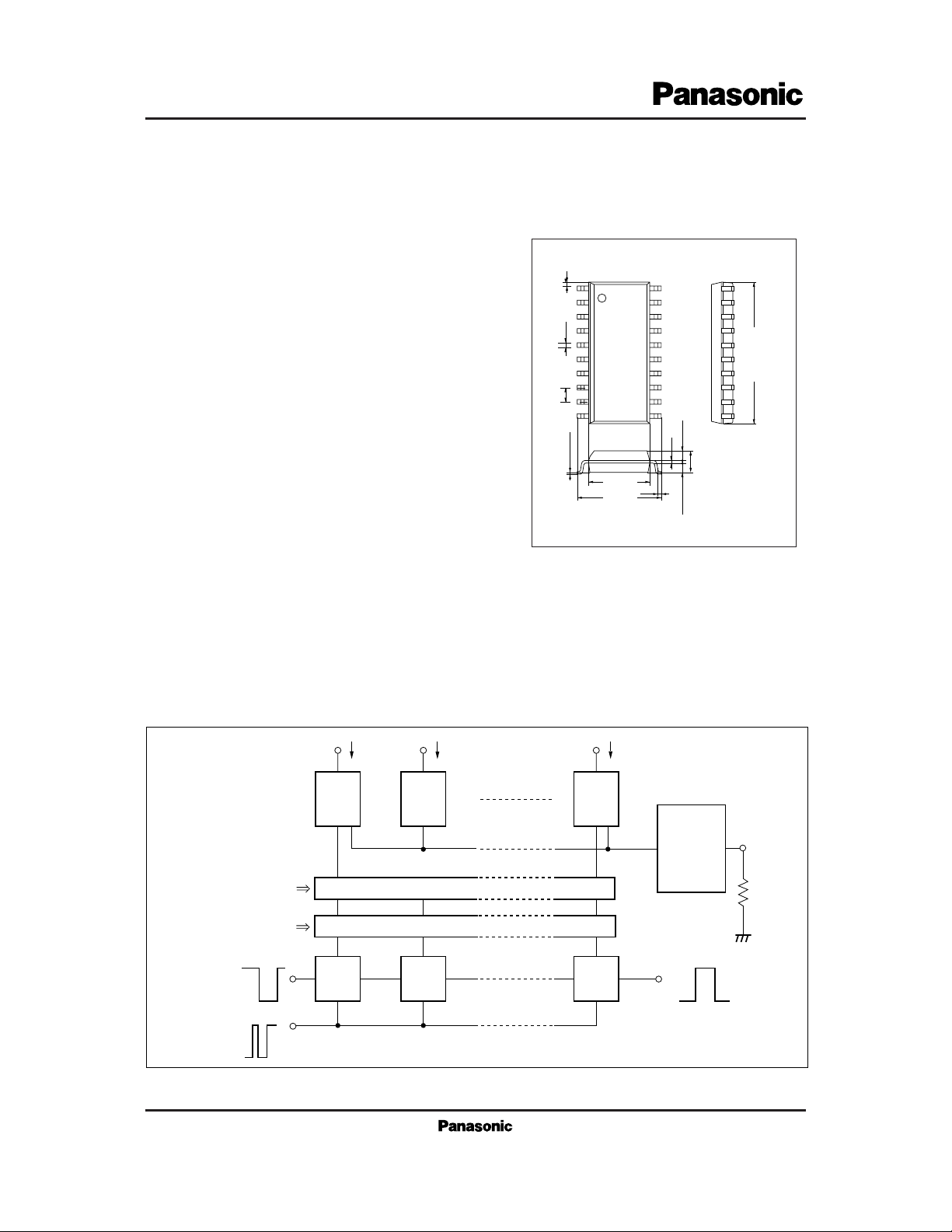
DN8667NS
8-Bit Shift Register Latch Constant Current Driver IC
1
2
3
4
5
6
7
8
9
10
20
19
18
17
16
15
14
13
12
11
5.5±0.3
7.6±0.3
(0.4)
1.27
0.9±0.25
2.05±0.2
0.9±0.25
0.2
– 0.05
+ 0.1
0.4±0.25 (0.4)
12.63±0.3
Unit : mm
0.1±0.1
20-pin SOP Package (SOP020-P-0300A)
■ Block Diagram
Gate Control Sig.
Latch Control Sig.
Data Input
Clock Input
12 8
Constant
Current
Output
Constant
Current
Output
Constant
Current
Output
Gate
Latch
Shift
Register
Shift
Register
Shift
Register
Current Set.
Data Output
Resistor
External
Page 2
2
OthersDN8667NS
Parameter Symbol Rating Unit
■ Absolute Maximum Rating (Ta = 25˚C)
*
For printed board SM, it decreases with rate of 10.24 mW/˚C from Ta = 25 ˚C.
Supply voltage
Output voltage
Output current
Power dissipation
*
Operating ambient temperature
Storage temperature
V
CC
V
O
I
O
P
D
T
opr
T
stg
0 to + 7.0
0 to + 14
150
1.28
–20 to + 85
–55 to + 150
V
V
mA
W
˚C
˚C
■ Recommended Operation Range (Ta=25 ˚C)
V
CC
Operating supply voltage
Parameter Symbol Range
4.5V to 5.5V
Note) VCC= 5V unless otherwise specified.
CLK
CLK
STB
SIN
STB
SIN
STB
Parameter Symbol Condition min typ max Unit
■ Electrical Characteristics (VCC=5V,Ta=25 ± 2˚C)
Input voltage
Positive direction
Negative direction
0.35V
CC
V
T+
0.7V
CC
V
V
SOUT
= 0.1, V
CC
– 0.1V
I
SOUT
= 20µA
Input current
0.2V
CC
4.0
83
20
20
20
15
20
10
V
T–
0.55V
CC
V
V
1H
= 5.0VI
IH
– 25
25
µA
mA
mA
mA
V
1L
= 0VI
IL
µA
µA
25
VO= 14V (Output OFF)I
OLK
2
mA
20
mA
MH
Z
ns
30
20
Output voltage (SOUT)
Output current 1 (Qn)
Output current 2 (Qn)
Output current error between bits
Output leak current
I
OH
= – 0.4mA
VCC=5.5V
V
OH
0.5
I
OL
= 1.6mAV
OL
I
ref
= 0mAI
CC1
I
ref
= –2.5mA
Input Duty 40 to 60%
I
CC2
I
ref
= –2.5mAI
CC3
f
CLK
t
w
t
su
t
h
t
r
t
f
100
117
V
O
(Qn) = 0.5V
I
OI
I
OI
±6
V
CC
= 5.0V, I
ref
= –12mA
V
O
(Qn) = 1.0V
DI
O
V
V
%
{
I
O
(Qn) = –10µA, 90mA
V
O
(Qn) =
0.6V I
ref
= –
2.5mA
{
Total Driver Output
OFF ON
Supply current
Input pulse width
Clock frequency
Setting-up time
Holding time
Clock pulse rise time
Clock pulse fall time
500
500
ns
ns
ns
ns
ns
ns
ns
V
CC
=5.0V
R
L
=50Ω
C
L
=15pF
Page 3

3
Others DN8667NS
Symbol Description
■ Pin Descriptions
* Calculation example
V
CC
= 5V
R
RC
= 910Ω
DGND
SIN
CLK
STB
Qn
Digital ground
It is the serial data input terminal for shift register.
The value of shift register shifts at the rising edge of clock input.
Pin No.
Pin name
1
2
3
4
5
Digital ground
Serial data input
Clock input
Strobe input
Driver output
7,8
10,11
13,14
16
9,12
15
20 × 5
910 + 90
I
O (
Qn
)
≈
** Calculation example
V
CC
= 5V
I
RC
= 0.0025A
I
O (
Qn
)
≈ 100mA
1 5
2 0.0025
R
RC
≈
R
RC
≈ 910
(Ω)
–180
V
CC (V)
2 × R
RC (Ω) +
180
I
RC
≈
(A)
V
CC (V)
I
RC (A)
or R
RC
≈
(Ω)
–180
20 × V
CC (V)
R
RC (Ω) +
90
I
O (
Qn
)
≈
(A)
1
2
Setting the STB input to "H" forwards the data of shift register to the latch.
When the STB input is set to "L" , even if the value of shift register changes,
the value of latch is not changed.
It outputs signals by using the polarity opposite to that of data taken into the
latch. For example, when the value of serial input is "H" , the output becomes
"L" level and the output is turned on. The output takes open collector form of
NPN transistor.
Output ground
When the EN input is set to "H" , all the outputs are turned off, independent of
condition of shift register or latch driver.
It is the terminal which performs the serial-output of data inputted from the SIN.
It connects the external resistor between RC and GND and sets the current of
output block.
* Output current calculation : ** RC terminal setting calculation :
Supply terminal
6
PGND
Output ground
17
EN
Enabling input
18
SOUT
Serial data output
19 RC
Constant current setting input
20
V
CC
V
CC
Page 4

4
OthersDN8667NS
DQ
CP
Q
DL
Q
DL
Q
DL
Q
DL
Q
DL
DN8667NS
SIN
V
CC
(20)
DGND
(1)
PGND
RC
(19)
V
LED
Current
setting
circuit
LED
Scan input
GND
LED
SOUT
(18)
SIN
(2)
CLK
(3)
ST B
(4)
EN
(17)
Q7
Q3Q2
Q1Q0
(16)(10)(8)(7)(5)
Logic
input
DN8667NS LED Panel Block Diagram
■ Application Circuit
(6) (9) (12) (15)
GND
LED
DQCPDQCPDQ
CP
DQ
CP
CLK
↑
↑
↑
↓
STB
H
L
×
×
EN
L
L
H
×
SIN
Q
n
Q
n
Q
n
Q
n
SOUT
Q
6
Q
6
Q
6
nc
Q
O
Q
n
nc
H
nc
Q
m
Q
m-1
nc
H
nc
Q
7
Q
6
nc
H
nc
Input Output
■ Function Table (Note)
H : High level,
L : Low level,
× : H or L
Qm, Qn : H or L.
However, for Qn, "H"= OFF, "L"= ON.
↑ : Shift from L to H,
↓ : Shift from H to L
nc : No change
(Note)
250 50 75 100 125 150
0
200
400
600
800
1000
1200
1400
1600
Power Dissipation P
D
(mW)
Ambient Temperature Ta (˚C)
PD — Ta
Glass epoxy printed board
(50mm
× 50mm × t0.8mm)
Rthj-a=97.7˚C/W
P
D
=1280 mW (25˚C)
Single unit
Rthj-a=174.1˚C/W
P
D
=718 mW (25˚C)
1280
718
■ Characteristics Curve
Page 5

5
Others DN8667NS
1.Input timing
5V
0V
5V
0V
5V
0V
CLK
SIN
STB
2.5V 2.5V
t
su(SIN)
t
h(SIN)
t
su(STB)
2.5V
2.5V
t
w(STB)
(VIL= 0V,VIH= 5.0V) (VIL= 0V,VIH= 5.0V)
90% 90%
2.5V 2.5V 2.5V
2.5V
2.5V
2.Transmission delay time
10% 10%
t
r(CLK)
t
f(CLK)
t
su(SIN)
t
h(SIN)
2.5V 2.5V
t
h(STB)
5V
0V
5V
0V
VOH
VOL
Qn
EN
CLK
2.5V 2.5V
t
PLH
50%50% 50%50%
t
PHL
t
PHL
t
WH (CLK)
t
WL(CLK)
1/fCLK
■ Timing Chart
t
PLH
 Loading...