

Datasheet DMV56-F5, DMV56, DMV32-F5, DMV32, DMV16-F5 Datasheet (SGS Thomson Microelectronics)
...Page 1
DMV series
®
August 1999 - Ed: 2A
DAMPER + MODULATION DIODE FOR VIDEO
Symbol Parameter
Value
Unit
MODUL DAMPER
V
RRM
Repetitive peak reverse voltage 600 1500 V
I
FSM
Surge non repetitive forward current tp = 10 m s
sinusoidal
DMV16 50 50 A
DMV32 60 75
DMV56 60 80
T
stg
Storage temperature range - 40 to + 150 °C
T
j
Maximum operating junction temperature 150
TURBOSWITCH is a trademark of STMicroelectronics
ABSOLUTE RATINGS
(limiting values, per diode)
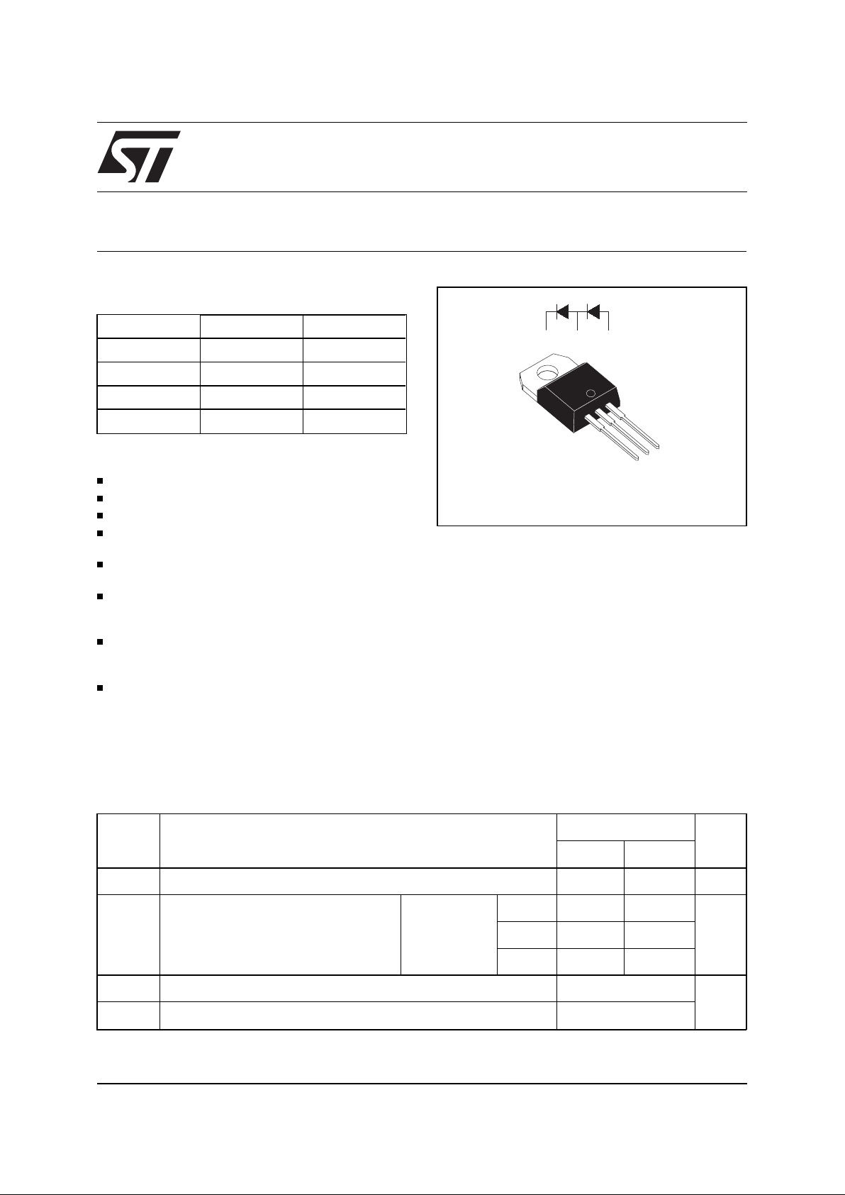
Insulated TO-220AB
(Bending option F5 available)
FULL KIT IN ONE PACKAGE
HIGH BREAKDOWN VOLTAGE CAPABILITY
VERY FAST RE COVE RY DIODE
SPECIFIED TURN ON SWITCHING
CHARACTERISTICS
LOW STATIC AND PEAK FORWARD
VOLT AG E DRO P FOR LOW DISSIP ATION
INSULATED VERSION:
Insulated voltage = 2500 V
RMS
Capacitance = 7 pF
PLANAR TECHNOLOGY ALLOW ING HIGH
QUALITY AND BEST ELECTRICAL
CHARACTERISTICS
OUTSTANDING PERFORMANCE OF WELL
PROVEN DTV AS DAMPER AND
TURBOSWITCH
TM
AS M ODULA TION
FEATURES AND BENE FITS
High voltage semiconductor especially designed
for horizontal deflection stage in standard and high
resolution video display with E/W correction.
The insulated TO-220AB package includes both
the DAMPER diode and the MODULATION diode.
Assembled on automated line, it offers excellent
insulating and dissipating characteristics, thanks to
the internal ceramic insulation layer.
DESCRIPTION
MODUL DAMPER
I
F(AV)
3 A & 6 A 5 A & 6 A
V
RRM
600 V 1500 V
t
rr
50 ns 135 ns
V
F
(max) 1.5 V 1.35 V
MAIN PRODUCT CHARACTERISTI CS
1
2
3
DAMPER MODULA TION
123
1/9
Page 2
Symbol Parameter
Value
Unit
DMV16 DMV32 DMV56
R
th(j-c)
Damper junction to case 5.3 4.8 3.6
°
C/W
R
th(j-c)
Modulation junction to case
6.5 5.3 5.3
R
th(c)
Coupling
0.2 0.2 0.2
R
th(j-c)
Total as per full I
F(AV)
maximum ratings 6.0 5.1 4.5
THERMAL RESISTANCES
Symbol Parameter Test conditions
Value
Unit
Tj = 25°C Tj = 125°C
Typ. Max. Typ. Max.
V
F
* Forward voltage drop IF = 5 A
DMV16
1.6 1.0 1.5 V
I
F
= 6 A
DMV32
1.5 1.1 1.35
I
F
= 6 A
DMV56
1.8 1.1 1.5
I
R
** Revers e leak age c urrent VR = V
RRM
DMV16
60 100 500
µ
A
DMV32
100 100 1000
DMV56
100 100 1000
Pulse test : * tp = 380 µs, δ < 2%
** tp = 5 ms, δ < 2%
To evaluate the maximum conduction losses of the DAMPER diode use the following equations :
DMV16: P = 1.14 x I
F(AV)
+ 0.072 x I
F2(RMS)
DMV32: P = 1.069 x I
F(AV)
+ 0.047 x I
F2(RMS)
DMV56: P = 1.15 x I
F(AV)
+ 0.059 x I
F2(RMS)
STATIC ELECTRICAL CHARACTE RISTICS OF THE DAMP ER DIODES
Symbol Parameter Test conditions
Value
UnitTj = 25°C Tj = 125°C
Typ. Max. Typ. Max.
V
F
* Forward voltage drop IF = 3A DMV16 1.4 1 1.3 V
I
F
= 5A DMV32 1.75 1.2 1.5
I
F
= 5A DMV56 1.75 1.2 1.5
I
R
**
Reverse leakage current V
R
= 480V
DMV16 20 150 500
µ
A
DMV32 100 600 2000
DMV56 100 600 2000
Pulse test : * tp = 380 µs, δ < 2%
** tp = 5 ms, δ < 2%
To evaluate the maximum conduction losses of the MODULATION diode use the following equations :
DMV16: P = 1.06 x I
F(AV)
+ 0.08x I
F2(RMS )
DMV32: P = 1.15 x I
F(AV)
+ 0.07 x I
F2(RMS)
DMV56: P = 1.15 x I
F(AV)
+ 0.07 x I
F2(RMS)
STATIC ELECTRICAL CHARACTERISTICS OF THE MODULATION DIODE
®
DMV series
2/9
Page 3
Symbol Parameter Test conditions
Value
Unit
Typ. Max.
t
rr
Revers e recovery t i me IF = 100mA
I
R
= 100mA
I
RR
= 10mA
Tj = 25° C
DMV16 1500 ns
DMV32 850
DMV56 750
t
rr
Revers e recovery t i me IF = 1A
dI
F
/dt = -50A/µs
V
R
= 30V
Tj = 25°C DMV16 200 300 ns
DMV32 130 175
DMV56 110 135
RECOVERY CHARAC TERISTICS OF THE DAM PER DIODE
Symbol Parameter Test conditions
Value
Unit
Typ. Max.
t
fr
Forward re covery ti me IF = 6A
dI
F
/dt = 80A/µs
V
FR
= 3V
Tj = 100°C
DMV16 350 ns
DMV32 570
DMV56 350
V
FP
Peak forward voltage IF = 6A
dI
F
/dt = 80A/µs
Tj = 100°C DMV16 25 34 V
DMV32 21 28
DMV56 19 26
TURN-ON SWITCHING CHARACT ERISTICS OF THE DAMPER DIODE
Symbol Parameter Test conditions
Value
Unit
Typ. Max.
t
rr
Revers e recovery t i me IF = 100mA
I
R
= 100mA
I
RR
= 10mA
Tj = 25°C DMV16 210 650 ns
DMV32 110 350
DMV56 110 350
t
rr
Revers e recovery t i me IF = 1A
dI
F
/dt = -50A/µs
V
R
= 30V
Tj = 25°C DMV16 95 ns
DMV32 50
DMV56 50
RECOVERY CHARAC TERISTICS OF THE MOD ULATION DIODE
Symbol Parameter Test conditions
Value
Unit
Typ. Max.
t
fr
Forward re covery ti me IF = 3A
dI
F
/dt = 80A/µs
V
FR
= 3V
Tj = 100°C DMV16 500 ns
I
F
= 5A
dI
F
/dt = 80A/µs
V
FR
= 3V
DMV32 300
DMV56 300
V
FP
Peak forward voltage IF = 3A
dI
F
/dt = 80A/µs
Tj = 100°C DMV16 8 V
I
F
= 5A
dI
F
/dt = 80A/µs
DMV32 10
DMV56 10
TURN-ON SWITCHING CHARACT ERISTICS OF THE MODULATION DIODE
®
DMV series
3/9
Page 4

ORDERING INFORMATION
DMVxx / F5
LEAD BENDING (OPTION)
DAMPER AND MODULATION DIODES FOR VIDEO
0123456
0.0
0.2
0.4
0.6
0.8
1.0
1.2
1.4
1.6
1.8
2.0
PF(av)(W)
DMV16
DMV32
DMV56
Ip(A)
Fig. 1-1:
Power dissipation versus peak forward
current (triangular waveform, δ=0.45) (damper
diode.)
0123456
0.0
0.2
0.4
0.6
0.8
1.0
1.2
1.4
1.6
1.8
2.0
PF(av)(W)
DMV16
DMV32/DMV56
Ip(A)
Fig. 1-2:
Power dissipation versus peak forward
current (triangular waveform, δ=0.45) (modulation
diode)
0 25 50 75 100 125 150
0
1
2
3
4
5
6
7
IF(av)(A)
Rth(j-a)=Rth(j-c)
DMV16
DMV32
DMV56
Tamb(°C)
T
δ
=tp/T
tp
Fig. 2-1:
Average forward current versus ambient
temperature (damper diode).
0 25 50 75 100 125 150
0
1
2
3
4
5
6
IF(av)(A)
DMV32/DMV56
DMV16
Rth(j-a)=Rth(j-c)
Tamb(°C)
T
δ
=tp/T
tp
Fig. 2-2:
Average forward current versus ambient
temperature (modulation diode).
®
DMV series
4/9
Page 5

0.0 0.2 0.4 0.6 0.8 1.0 1.2 1.4 1.6 1.8 2.0 2.2
0.1
1.0
10.0
20.0
IFM(A)
Typ ical
Tj=125°C
Maximum
Tj=25°C
Maximum
Tj=125°C
VFM(V)
Fig. 3-1:
Forward voltage drop versus forward
current (damper diode) DMV16.
0.0 0.2 0.4 0.6 0.8 1.0 1.2 1.4 1.6 1.8 2.0 2.2 2.4 2.6 2.8
0.1
1.0
10.0
50.0
IFM(A)
Typ ical
Tj=125°C
Maximum
Tj=25°C
Maximum
Tj=125°C
VFM(V)
Fig. 3-2:
Forward voltage drop versus forward
current (damper diode)DMV32.
0.0 0.2 0.4 0.6 0.8 1.0 1.2 1.4 1.6 1.8 2.0 2.2 2.4 2.6 2.8
0.1
1.0
10.0
50.0
IFM(A)
Typ ical
Tj=125°C
Maximum
Tj=25°C
Maximum
Tj=125°C
VFM(V)
Fig. 3-3:
Forward voltage drop versus forward
current (damper diode)DMV56.
0.0 0.2 0.4 0.6 0.8 1.0 1.2 1.4 1.6 1.8 2.0 2.2
0.1
1.0
10.0
20.0
IFM(A)
Typ ical
Tj=125°C
Maximum
Tj=25°C
Maximum
Tj=125°C
VFM(V)
Fig. 3-4:
Forward voltage drop versus forward
current (modulation diode)DMV16.
0.0 0.2 0.4 0.6 0.8 1.0 1.2 1.4 1.6 1.8 2.0 2.2
0.1
1.0
10.0
20.0
IFM(A)
Typ ical
Tj=125°C
Maximum
Tj=25°C
Maximum
Tj=125°C
VFM(V)
Fig. 3-5:
Forward voltage drop versus forward
current (modulation diode)DMV32 and DMV56.
1E-3 1E-2 1E-1 1E+0
0.1
0.2
0.5
1.0
K=[Zth(j-c)/Rth(j-c)]
tp(s)
T
δ
=tp/T
tp
Single pulse
δ = 0.1
δ = 0.2
δ = 0.5
Fig. 4:
Relative variation of thermal impedance
junction to case versus pulse duration.
®
DMV series
5/9
Page 6

1E-3 1E-2 1E-1 1E+0
0
5
10
15
20
25
30
35
40
IM(A)
Tc=100°C
DMV16
DMV32/DMV56
I
M
t
δ
=0.5
t(s)
Fig. 5-2:
Non repetitive surge peak forward current
versus overload duration (modulation diode).
1E-3 1E-2 1E-1 1E+0
0
5
10
15
20
25
30
35
40
45
IM(A)
Tc=100°C
DMV56
DMV32
DMV16
t(s)
I
M
t
δ
=0.5
Fig. 5-1:
Non repetitive surge peak forward current
versus overload duration (damper diode).
0.1 0.2 0.5 1.0 2.0 5.0
0.0
0.2
0.4
0.6
0.8
1.0
1.2
1.4
1.6
1.8
2.0
2.2
2.4
Qrr(µC)
IF=IF(av)
90% confidence
Tj=125°C
DMV56
DMV32
DMV16
dIF/dt(A/µs)
Fig. 6-1:
Reverse recovery charges versus d
IF
/dt
(damper diode).
0.1 1.0 10.0 50.0
0
50
100
150
200
250
300
350
400
450
500
Qrr(nC)
IF=IF(av)
90% confidence
Tj=125°C
DMV32/DMV56
DMV16
dIF/dt(A/µs)
Fig. 6- 2:
Reverse recovery charges versus d
IF
/dt
(modulation diode).
0.1 0.2 0.5 1.0 2.0 5.0
0.0
0.5
1.0
1.5
2.0
2.5
3.0
IRM(A)
IF=IF(av)
90% confidence
Tj=125°C
DMV16
DMV32
DMV56
dIF/dt(A/µs)
Fig. 7-1:
Reverse recovery current versus d
IF
/dt
(damper diode).
0.1 1.0 10.0 100.0
0
1
2
3
4
5
6
7
8
9
10
IRM(A)
IF=IF(av)
90% confidence
Tj=125°C
DMV32/DMV56
DMV16
dIF/dt(A/µs)
Fig. 7-2:
Reverse recovery current versus d
IF
/dt
(modulation diode).
®
DMV series
6/9
Page 7

0 20 40 60 80 100 120 140
0
5
10
15
20
25
30
35
40
45
50
VFP(V)
IF=IF(av)
90% confidence
Tj=125°C
DMV16
DMV32
DMV56
dIF/dt(A/µs)
Fig. 8-1:
Transient peak forward voltage versus
d
IF
/dt (damper diode).
0 20 40 60 80 100 120 140 160 180 200
0
2
4
6
8
10
12
14
16
18
20
VFP(V)
IF=IF(av)
90% confidence
Tj=125°C
DMV32/DMV56
DMV16
dIF/dt(A/µs)
Fig. 8-2:
Transient peak forward voltage versus
d
IF
/dt (modulation diode).
0 20 40 60 80 100 120 140
200
250
300
350
400
450
500
550
600
650
700
tfr(ns)
IF=IF(av)
90% confidence
Tj=125°C
Vfr=3V
DMV16/DMV32/DMV56
dIF/dt(A/µs)
Fig. 9-1:
Forward recovery time versus d
IF
/dt
(damper diode).
0 20 40 60 80 100 120 140 160 180 200
0
50
100
150
200
250
300
350
400
tfr(ns)
IF=IF(av)
90% confidence
Tj=125°C
Vfr=1.5V
DMV32/DMV56
DMV16
dIF/dt(A/µs)
Fig. 9-2:
Forward recovery time versus d
IF
/dt
(modulation diode).
0 20 40 60 80 100 120 140
0.0
0.2
0.4
0.6
0.8
1.0
1.2
VFP,IRM,Qrr[Tj] /VFP,IRM,Qrr[Tj=125°C]
VFP
IRM
Qrr
Tj(°C)
Fig. 10:
Dynamic parameters versus junction
temperature (damper & modulation diodes).
1 10 100 200
1
10
100
VR(V)
C(pF)
Tj=25°C
F=1MHz
Damper diodes
Modulation diodes
DMV16
DMV32
DMV56
DMV16
DMV32/DMV56
Fig. 11:
Junction capacitance versus reverse
voltage applied (typical values).
®
DMV series
7/9
Page 8

PACKAGE MEC HANICAL DA TA
TO-220AB F5 OPTION
REF.
DIMENSIONS
Millimeters Inches
Min. Max. Min. Max.
A 15.20 15.90 0.598 0.625
a1 24.16 26.90 0.951 1.059
a3 1.65 2.41 0.064 0.094
B 10.00 10.40 0.393 0.409
b1 0.61 0.88 0.024 0.034
b2 1.23 1.32 0.048 0.051
C 4.40 4.60 0.173 0.181
c1 0.49 0.70 0.019 0.027
c2 2.40 2.72 0.094 0.107
e 2.40 2.70 0.094 0.106
F 6.20 6.60 0.244 0.259
I 3.75 3.85 0.147 0.151
L 2.65 2.95 0.104 0.116
I2 1.14 1.70 0.044 0.066
l3 1.14 1.70 0.044 0.066
l4 15.80 16.80 0.622 0.661
16.40 typ. 0.645 typ.
M1 2.92 3.30 0.114 0.129
R1 1.40 typ. 0.055 typ.
R2 1.40 typ. 0.055 typ.
c2
B
a1
C
b2
l2
c2
a3
R2
R1
l3
b1
l4
A
F
L
I
e
c1
M1
Ø
cooling method: by conduction (c)
Recommended torque value: 0.8 m.N.
Maximum torque value: 1 m.N.
2.2mm
2.54mm
1mm
3.1mm
PRINTED CIRCUIT LAYOUT FOR F5 LAYOUT
®
DMV series
8/9
Page 9

Information furnished is believed to be accurate and reliable. However, STMicroelectronics assumes no responsibility for the consequences of
use of such information nor for any infringement of patents or other rights of third parties which may result from its use. No license is granted by
implication o r otherw ise under any p atent or pat ent ri ghts of STMi croelec tronics. Specificat ions ment ioned in this publicati on are subject to
change without notice. This publication supersedes and replaces all information previously supplied.
STMicroelectr oni cs products are not authorized for use as critical c om ponents i n l i fe s upport devices or systems without express written a pproval of STMicroelectronics.
The ST logo is a registered trademark of STMicroel ectronics
© 1999 STMicroelectronics - Printed in Italy - All rights reserved.
STMicroelectronics GROUP OF COMPANIES
Australia - Brazil - China - Finland - France - Germany - Hong Kong - India - Italy - Japan - Malaysia
Malta - Morocco - Singapore - Spain - Sweden - Switzerland - United Kingdom - U.S.A.
http://www.st.com
Type M arking Package Weight Base q ty Delivery mode
DMV16
DMV16/F5
DMV16 TO-220AB 2.2 g. 50 Tube
DMV32
DMV32/F5
DMV32 TO-220AB 2.2 g. 50 Tube
DMV56
DMV56/F5
DMV56 TO-220AB 2.2 g. 50 Tube
Epoxy meets UL94, V0
PACKAGE ME CHANICAL D AT A
TO-220AB
M
B
l4
C
b2
a2
l2
c2
l3
b1
a1
A
F
L
I
e
c1
REF.
DIMENSIONS
Millimeters Inches
Min. Typ. Max. Min. Typ. Max.
A 15.20 15.90 0.598 0.625
a1 3.75 0.147
a2 13.00 14.00 0.511 0.551
B 10.00 10.40 0.393 0.409
b1 0.61 0.88 0.024 0.034
b2 1.23 1.32 0.048 0.051
C 4.40 4.60 0.173 0.181
c1 0.49 0.70 0.019 0.027
c2 2.40 2.72 0.094 0.107
e 2.40 2.70 0.094 0.106
F 6.20 6.60 0.244 0.259
I 3.75 3.85 0.147 0.151
I4 15.80 16.40 16.80 0.622 0.646 0.661
L 2.65 2.95 0.104 0.116
l2 1.14 1.70 0.044 0.066
l3 1.14 1.70 0.044 0.066
M 2.60 0.102
cooling method: by conduc tion (c)
Recommended torque value: 0.8 m.N.
Maximum torque value: 1 m.N.
®
DMV series
9/9
 Loading...