

Page 1
®
DMV1500H
DAMPER + MODULATION DIODE FOR VIDEO
MAIN PRODUCT CHARACTERISTICS
MODUL DAMPER
I
F(AV)
V
RRM
t
(max) 50 ns 125ns
rr
V
(max) 1.4 V 1.7 V
F
3A 6A
600 V 1500 V
FEATURES AND BENEFITS
Fullkitinonepackage
■
■ High breakdown voltage capability
■ Very fast recovery diode
■ Specified turn on switching characteristics
■
Low static and peak forward voltage dropfor low
dissipation
■ Insulated version:
Insulated voltage = 2500 V
RMS
Capacitance = 7 pF
■
Planar technology allowing high quality and
best electrical characteristics
■
Outstanding performance of well proven DTV
as damper and new faster Turbo 2 600V
technology as modulation
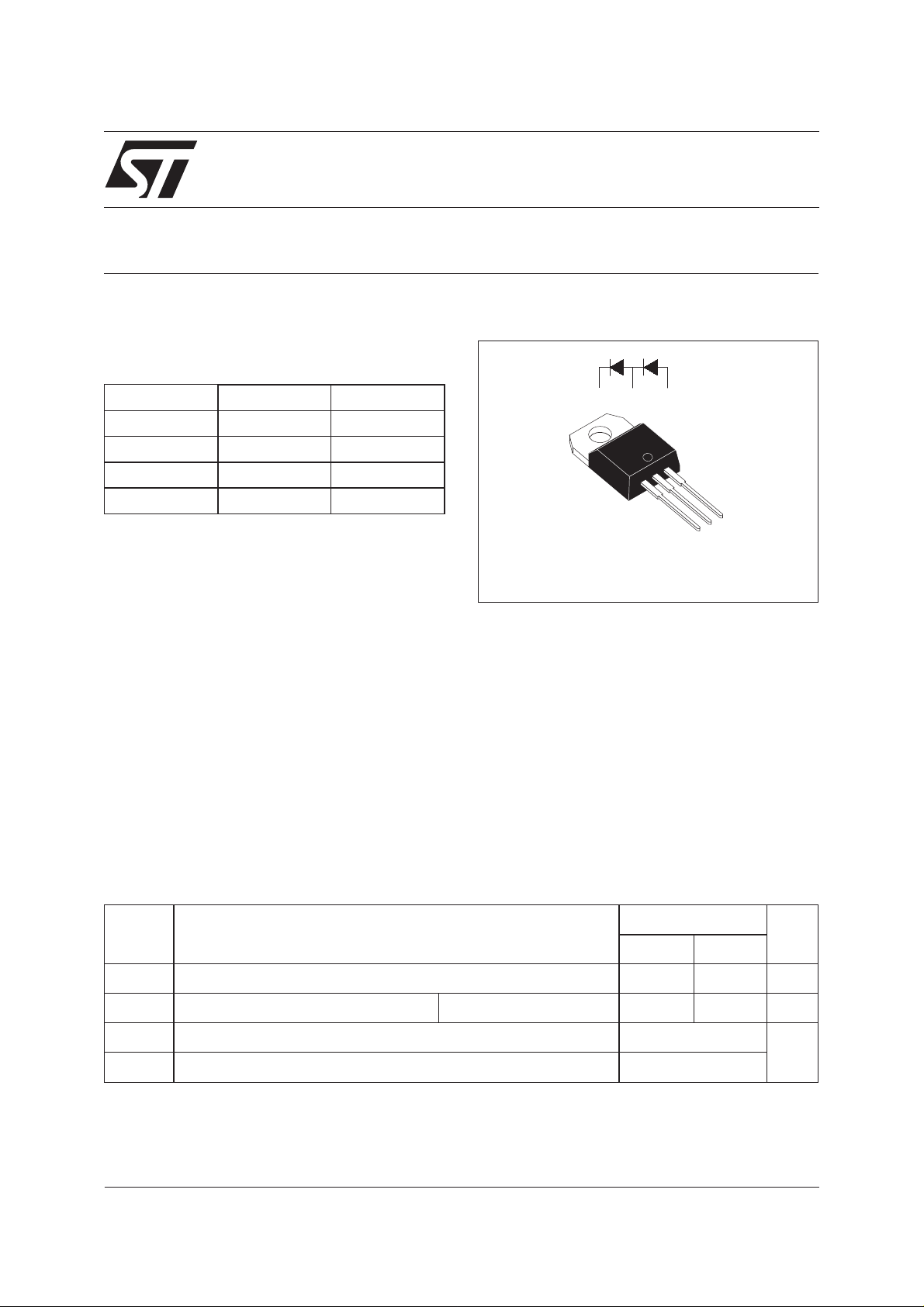
DAMPER MODULATION
123
3
2
1
Insulated TO-220AB
(Bending option F5 available)
DESCRIPTION
High voltage semiconductor especially designed
for horizontal deflection stageinstandardandhigh
resolution video display with E/W correction.
The insulated TO-220AB package includes both
theDAMPERdiodeandthe MODULATION diode.
Assembled on automated line, it offers excellent
insulating and dissipating characteristics, thanks
to the internal ceramic insulation layer.
ABSOLUTE RATINGS (limiting values, per diode)
Symbol Parameter
V
RRM
I
FSM
T
stg
T
July 2001 - Ed: 6A
Repetitive peak reverse voltage
Surge non repetitive forward current tp = 10 ms sinusoidal
Storage temperature range
Maximum operating junction temperature
j
Value
Unit
MODUL DAMPER
600 1500 V
35 80 A
-40to+150 °C
150
1/9
Page 2
DMV1500H
THERMAL RESISTANCES
Symbol Parameter Value Unit
R
th(j-c)
R
th(j-c)
STATIC ELECTRICAL CHARACTERISTICS OF THE DAMPER DIODES
Damper junction to case
Modulation junction to case
3.6 °C/W
6
Value
Symbol Parameter Test conditions
Typ. Max. Typ. Max.
Forward voltage drop I
*
V
F
**
I
R
Pulse test : * tp = 380 µs, δ <2%
To evaluate the maximum conduction losses of the DAMPER diode use the following equations :
P=1.35xI
Reverse leakage current V
**tp = 5 ms, δ <2%
+ 0.059 x I
F(AV)
F2(RMS)
=6A
F
= 1500V
R
1.5 2.3 1.25 1.7 V
100 100 1000 µA
STATIC ELECTRICAL CHARACTERISTICS OF THE MODULATION DIODE
Value
Symbol Parameter
Test
conditions
Typ. Max. Typ. Max.
Forward voltage drop I
*
V
F
**
I
R
Pulse test : * tp = 380 µs, δ <2%
To evaluate the maximum conduction losses of the MODULATION diode use the following equations :
P=1.2xI
Reverse leakage current V
** tp = 5 ms, δ <2%
+ 0.066 x I
F(AV)
F2(RMS)
=3A
F
= 600V
R
1.8 1.1 1.4 V
20350µA
UnitTj = 25°C Tj = 125°C
UnitTj = 25°C Tj = 125°C
RECOVERY CHARACTERISTICS OF THE DAMPER DIODE
Symbol Parameter Test conditions
Tj = 25°C
Tj = 25°C
2/9
t
rr
t
rr
Reverse recovery time IF= 100mA
= 100mA
I
R
= 10mA
I
RR
Reverse recovery time IF=1A
/dt = -50A/µs
dI
F
= 30V
V
R
Value
Typ. Max.
Unit
625 ns
95 125 ns
®
Page 3

RECOVERY CHARACTERISTICS OF THE MODULATION DIODE
DMV1500H
Symbol Parameter Test conditions
t
rr
t
rr
Reverse recovery time IF= 100mA
= 100mA
I
R
= 10mA
I
RR
Reverse recovery time IF=1A
/dt = -50A/µs
dI
F
= 30V
V
R
Tj = 25°C
Tj = 25°C
TURN-ON SWITCHING CHARACTERISTICS OF THE DAMPER DIODE
Symbol Parameter Test conditions
t
fr
V
FP
Forward recovery time IF=6A
/dt = 80A/µs
dI
F
=3V
V
FR
Peak forward voltage IF=6A
/dt = 80A/µs
dI
F
Tj = 100°C
Tj = 100°C
TURN-ON SWITCHING CHARACTERISTICS OF THE MODULATION DIODE
Value
Typ. Max.
Unit
110 350 ns
50 ns
Value
Typ. Max.
Unit
350 ns
18 25 V
Symbol Parameter Test conditions
t
fr
V
FP
Forward recovery time IF=3A
/dt = 80A/µs
dI
F
=2V
V
FR
Peak forward voltage IF=3A
/dt = 80A/µs
dI
F
Tj = 100°C
Tj = 100°C
Value
Typ. Max.
240 ns
8V
Unit
®
3/9
Page 4

DMV1500H
Fig. 1-1: Power dissipation versus peak forward
current (triangular waveform, δ = 0.45) (damper
diode).
PF(av)(W)
2.2
2.0
1.8
1.6
1.4
1.2
1.0
0.8
0.6
0.4
0.2
0.0
0123456
Ip(A)
Fig. 2-1: Average forward current versus ambient
temperature (damper diode).
IF(av)(A)
8
7
6
5
4
3
2
1
=tp/T
δ
0
0 25 50 75 100 125 150
T
Rth(j-a)=Rth(j-c)
tp
Tamb(°C)
Fig. 1-2: Power dissipation versus peak forward
current (triangular waveform, δ = 0.45) (modulation diode).
PF(av)(W)
2.2
2.0
1.8
1.6
1.4
1.2
1.0
0.8
0.6
0.4
0.2
0.0
0123456
Ip(A)
Fig. 2-2: Average forward current versus ambient
temperature (modulation diode).
IF(av)(A)
4.0
3.5
3.0
2.5
2.0
1.5
δ
=tp/T
T
tp
Tamb(°C)
1.0
0.5
0.0
0 25 50 75 100 125 150
Rth(j-a)=Rth(j-c)
Fig. 3-1: Forward voltage drop versus forward
current (damper diode).
IFM(A)
15.0
Typical
Tj=125°C
10.0
Maximum
Tj=125°C
5.0
VFM(V)
0.4 0.6 0.8 1.0 1.2 1.4 1.6 1.8 2.0 2.2 2.4 2.6 2.8
4/9
Maximum
Tj=25°C
Fig. 3-2: Forward voltage drop versus forward
current (modulation diode).
IFM(A)
10.0
9.0
8.0
7.0
6.0
5.0
4.0
3.0
2.0
1.0
0.4 0.6 0.8 1.0 1.2 1.4 1.6 1.8 2.0 2.2 2.4 2.6 2.8 3.0
Maximum
Tj=125°C
Typical
Tj=125°C
VFM(V)
Maximum
Tj=25°C
®
Page 5

DMV1500H
Fig. 4: Relative variation of thermal impedance
junction to case versus pulse duration.
K=[Zth(j-c)/Rth(j-c)]
1.0
δ = 0.5
0.5
δ = 0.2
δ = 0.1
0.2
Single pulse
tp(s)
0.1
1E-3 1E-2 1E-1 1E+0
δ
=tp/T
T
tp
Fig.5-2: Non repetitivesurge peak forward current
versus overload duration (modulation diode).
IM(A)
30
25
20
15
10
IM
5
0
1E-3 1E-2 1E-1 1E+0
δ=0.5
t
t(s)
Tc=100°C
Fig.5-1: Non repetitivesurge peak forward current
versus overload duration (damper diode).
IM(A)
40
Tc=100°C
35
30
25
20
15
10
IM
5
0
1E-3 1E-2 1E-1 1E+0
δ=0.5
t
t(s)
Fig. 6-1: Reverse recovery charges versus dIF/dt
(damper diode).
Qrr(nc)
1200
1000
800
600
400
200
IF= 6A
90% confidence
Tj=125°C
dIF/dt(A/µs)
0
0.1 0.2 0.5 1.0 2.0 5.0
Fig. 6-2: Reverse recovery charges versus dIF/dt
(modulation diode).
Qrr(nC)
200
150
100
IF= 3A
90% confidence
Tj=125°C
50
dIF/dt(A/µs)
0
0.1 1.0 10.0 100.0
®
Fig. 7-1: Reverse recovery current versus dIF/dt
(damper diode).
IRM(A)
2.4
2.2
2.0
1.8
1.6
1.4
1.2
1.0
0.8
0.6
0.4
0.2
0.0
IF= 6A
90% confidence
Tj=125°C
dIF/dt(A/µs)
0.1 0.2 0.5 1.0 2.0 5.0
5/9
Page 6

DMV1500H
Fig. 7-2: Reverse recovery current versus dIF/dt
(modulation diode).
IRM(A)
6
IF= 3A
90% confidence
Tj=125°C
5
4
3
2
1
dIF/dt(A/µs)
0
1 10 100 200
Fig. 8-2: Transient peak forward voltage versus
dIF/dt (modulation diode).
VFP(V)
12
IF= 3A
11
90% confidence
Tj=125°C
10
9
8
7
6
5
4
3
2
1
0
0 20 40 60 80 100 120 140 160 180 200
dIF/dt(A/µs)
Fig. 8-1: Transient peak forward voltage versus
dIF/dt (damper diode).
VFP(V)
40
IF= 6A
90% confidence
35
Tj=125°C
30
25
20
15
10
5
0
0 20 40 60 80 100 120 140
dIF/dt(A/µs)
Fig. 9-1: Forward recovery time versus dIF/dt
(damper diode).
tfr(ns)
800
750
700
650
600
550
500
450
400
350
300
0 20 40 60 80 100 120 140
dIF/dt(A/µs)
IF= 6A
90% confidence
Tj=125°C
VFR=3V
Fig. 9-2: Forward recovery time versus dIF/dt
(modulation diode).
tfr(ns)
200
175
150
125
100
75
50
25
0
0 20 40 60 80 100 120 140 160 180 200
dIF/dt(A/µs)
6/9
IF= 3A
90% confidence
Tj=125°C
Vfr=2V
Fig. 10: Dynamic parameters versus junction temperature (damper & modulation diodes).
VFP,IRM,Qrr[Tj]/VFP,IRM,Qrr[Tj=125°C]
1.2
1.0
0.8
VFP
0.6
IRM
0.4
Qrr
0.2
0.0
0 20 40 60 80 100 120 140
Tj(°C)
®
Page 7

DMV1500H
Fig. 11: Junction capacitance versus reverse voltage
applied (typical values) (damper & modulation
diodes).
C(pF)
100
Tj=25°C
F=1MHz
10
1
1 10 100 200
Modulation
VR(V)
ORDERING INFORMATION
DMV1500H / F5
LEAD BENDING (OPTION)
DAMPER AND MODULATION DIODES FORVIDEO
®
7/9
Page 8

DMV1500H
PACKAGE MECHANICAL DATA
TO-220AB F5 OPTION
B
Ø
I
a1
l3
l2
b1
e
b2
L
A
l4
DIMENSIONS
REF.
Millimeters Inches
Min. Max. Min. Max.
A 15.20 15.90 0.598 0.625
C
a1 24.16 26.90 0.951 1.059
a3 1.65 2.41 0.064 0.094
B 10.00 10.40 0.393 0.409
F
b1 0.61 0.88 0.024 0.034
b2 1.23 1.32 0.048 0.051
C 4.40 4.60 0.173 0.181
c1 0.49 0.70 0.019 0.027
c2 2.40 2.72 0.094 0.107
R2
c2
a3
R1
e 2.40 2.70 0.094 0.106
F 6.20 6.60 0.244 0.259
I 3.75 3.85 0.147 0.151
L 2.65 2.95 0.104 0.116
c2
c1
M1
I2 1.14 1.70 0.044 0.066
l3 1.14 1.70 0.044 0.066
l4 15.80 16.80 0.622 0.661
16.40 typ. 0.645 typ.
M1 2.92 3.30 0.114 0.129
R1 1.40 typ. 0.055 typ.
R2 1.40 typ. 0.055 typ.
PRINTED CIRCUIT LAYOUT FOR F5 LAYOUT
3.1mm
8/9
1mm
2.2mm
2.54mm
■
Cooling method: by conduction (c)
■
Recommended torque value: 0.8 m.N.
■
Maximum torque value: 1 m.N.
®
Page 9

PACKAGE MECHANICAL DATA
TO-220AB
B
L
I
A
l4
a1
l3
l2
a2
b1
e
DMV1500H
DIMENSIONS
C
b2
A 15.20 15.90 0.598 0.625
a1 3.75 0.147
REF.
F
a2 13.00 14.00 0.511 0.551
B 10.00 10.40 0.393 0.409
b1 0.61 0.88 0.024 0.034
b2 1.23 1.32 0.048 0.051
C 4.40 4.60 0.173 0.181
c1 0.49 0.70 0.019 0.027
c2
c2 2.40 2.72 0.094 0.107
e 2.40 2.70 0.094 0.106
F 6.20 6.60 0.244 0.259
I 3.75 3.85 0.147 0.151
I4 15.80 16.40 16.80 0.622 0.646 0.661
M
c1
L 2.65 2.95 0.104 0.116
l2 1.14 1.70 0.044 0.066
l3 1.14 1.70 0.044 0.066
M 2.60 0.102
Millimeters Inches
Min. Typ. Max. Min. Typ. Max.
■ Cooling method: by conduction (c)
■
Recommended torque value: 0.8 m.N.
■
Maximum torque value: 1 m.N.
Type Marking Package Weight Base qty Delivery mode
DMV1500H
DMV1500H TO-220AB 2.2g. 50 Tube
DMV1500HF5
■
Epoxy meets UL94, V0
Informationfurnished is believed to be accurate andreliable. However, STMicroelectronics assumes no responsibility forthe consequences of
useof such information nor for anyinfringement of patents or other rights ofthird parties which may result fromits use. No license is granted by
implication or otherwise under any patent or patent rights of STMicroelectronics. Specifications mentioned in this publication are subject to
change without notice. This publication supersedes and replaces all information previously supplied.
STMicroelectronics products are not authorized for use as critical components in life support devices or systems without express written approval of STMicroelectronics.
The ST logo is a registered trademark of STMicroelectronics
© 2001 STMicroelectronics - Printed in Italy - All rights reserved.
STMicroelectronics GROUP OF COMPANIES
Australia - Brazil - China - Finland - France - Germany - Hong Kong - India - Italy - Japan - Malaysia
Malta - Morocco - Singapore - Spain - Sweden - Switzerland - United Kingdom - U.S.A.
http://www.st.com
®
9/9
 Loading...