

Page 1
© 2000 Fairchild Semiconductor Corporation DS006494 www.fairchildsemi.com
August 1986
Revised February 2000
DM7404 Hex Inverting Gates
DM7404
Hex Inverting Gat e s
General Description
This device contain s six independe nt gates eac h of which
performs the logic INVERT function.
Ordering Code:
Devices also availab le in Tape and Reel. Specify by appending th e s uffix let t er “X” to the ordering code.
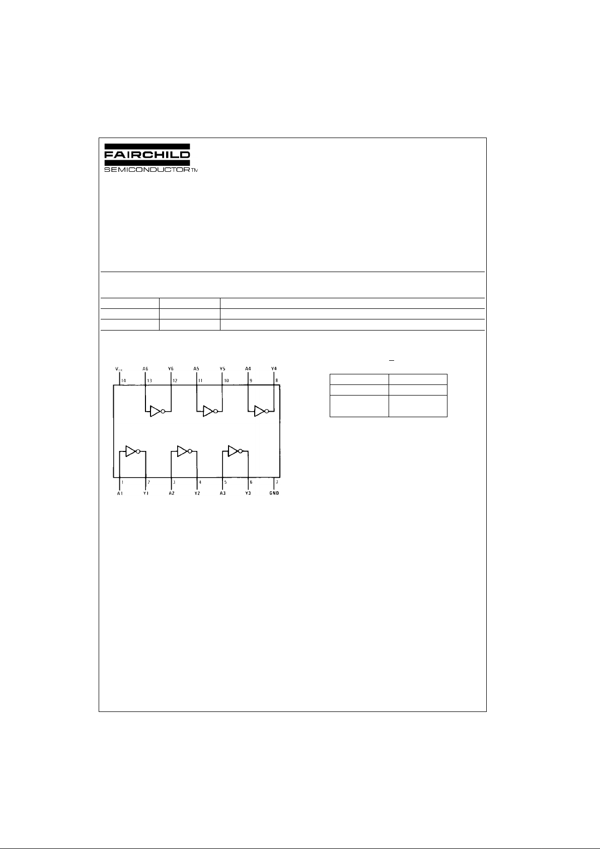
Connection Diagram Function Table
Y = A
H = HIGH Logic Level
L = LOW Logic Level
Order Number Package Number Package Description
DM7404M M14A 14-Lead Small Outline Integrated Circuit (SOIC), JEDEC MS-012, 0.150 Narrow
DM7404N N14A 14-Lead Plastic Dual-In-Line Package (PDIP), JEDEC MS-001, 0.300 Wide
Inputs Output
AY
LH
HL
Page 2
www.fairchildsemi.com 2
DM7404
Absolute Maximum Ratings(Note 1)
Note 1: The “Absolute Maximum Ratings” are those values beyond which
the safety of the dev ice cannot be guaranteed. T he device sh ould not be
operated at these limits. The parametric values defined in the Electrical
Characteristics tables are not guaranteed at the absolute maximum ratings.
The “Recommend ed O peratin g Cond itions” t able w ill defin e the co ndition s
for actual device operation.
Recommended Operating Conditions
Electrical Characteristics
over recommended operating free air temperature range (unless otherwise noted)
Note 2: All typicals are at VCC = 5V, TA = 25°C.
Note 3: Not more than one output should be shorted at a time.
Switching Characteristics
at VCC = 5V and TA = 25°C
Supply Voltage 7V
Input Voltage 5.5V
Operating Free Air Temperature Range 0°C to +70°C
Storage Temperature Range −65°C to +150°C
Symbol Parameter Min Nom Max Units
V
CC
Supply Voltage 4.75 5 5.25 V
V
IH
HIGH Level Input Voltage 2 V
V
IL
LOW Level Input Voltage 0.8 V
I
OH
HIGH Level Output Current −0.4 mA
I
OL
LOW Level Output Current 16 mA
T
A
Free Air Operating Temperature 0 70 °C
Symbol Parameter Conditions Min
Typ
Max Units
(Note 2)
V
I
Input Clamp Voltage VCC = Min, II = −12 mA −1.5 V
V
OH
HIGH Level VCC = Min, IOH = Max
2.4 3.4 V
Output Voltage VIL = Max
V
OL
LOW Level VCC = Min, IOL = Max
0.2 0.4 V
Output Voltage VIH = Min
I
I
Input Current @ Max Input Voltage VCC = Max, VI = 5.5V 1 mA
I
IH
HIGH Level Input Current VCC = Max, VI = 2.4V 40 µA
I
IL
LOW Level Input Current VCC = Max, VI = 0.4V −1.6 mA
I
OS
Short Circuit Output Current VCC = Max (Note 3) −18 −55 mA
I
CCH
Supply Current with Outputs HIGH VCC = Max 6 12 mA
I
CCL
Supply Current with Outputs LOW VCC = Max 18 33 mA
Symbol Parameter Conditions Min Max U ni ts
t
PLH
Propagation Delay Time CL = 15 pF
22 ns
LOW-to-HIGH Level Output RL = 400Ω
t
PHL
Propagation Delay Time
15 ns
HIGH-to-LOW Level Output
Page 3

3 www.fairchildsemi.com
DM7404
Physical Dimensions inches (millimeters) unless otherwise noted
14-Lead Small Outline Integrated Circuit (SOIC), JEDEC MS-012, 0.150 Narrow
Package Number M14A
Page 4

www.fairchildsemi.com 4
DM7404 Hex Inverting Gates
Physical Dimensions inches (millimeters) unless otherwise noted (Continued)
14-Lead Plastic Dual-In-Line Package (PDIP), JEDEC MS-001, 0.300 Wide
Package Number N14A
Fairchild does not assume any responsibility for use of any circuitry described, no circuit pate nt licenses are implied and
Fairchild reserves the right at any time without notice to change said circuitry and specifications.
LIFE SUPPORT POLICY
FAIRCHILD’S PRODUCTS ARE NOT AUTHORIZED FOR USE AS CRITICAL COMPONENTS IN LIFE SUPPORT
DEVICES OR SYSTEMS WITHOUT THE EXPRESS WRITTEN APPROVAL OF THE PRESIDENT OF FAIRCHILD
SEMICONDUCTOR CORPORATION. As used herein:
1. Life support devices or systems are devices or syste ms
which, (a) are intended for surgical implant into the
body, or (b) support or sustain life, and (c) whose failure
to perform when properly used in accordance with
instructions for use provided in the labeling, can be reasonably expected to result in a significant inju ry to the
user.
2. A critical component i n any compon ent of a lif e support
device or system whose failu re to perform can be reasonably expected to ca use the fa i lure of the life su pp ort
device or system, or to affect its safety or effectiveness.
www.fairchildsemi.com
 Loading...