

Page 1
DM560P
V.90 Integrated Data/Fax/Voice/Speakerphone Modem Device Set
General Description
The DM560P integrated modem is a four chipset
design that provides a complete solution for stateof-the-art, voice-band Plain Old Telephone Service
(POTS) communication. The modem provides for
Data (up to 56,000bps), Fax (up to 14,400bps),
Voice and Full Duplex Speaker-phone functions to
comply with various international standards.
The design of the DM560P is optimized for desktop
personal computer applications and it provides a low
cost, highly reliable, maximum integration, with the
minimum am ount of support required. The DM560P
modem can operate over a dial-up network (PSTN)
or 2 wire leased lines.
The modem integrates auto dial and answer
capabilities, synchronous and asynchronous data
transmi ssions, seri al and parallel interfaces, various
tone detection schemes and data test modes.
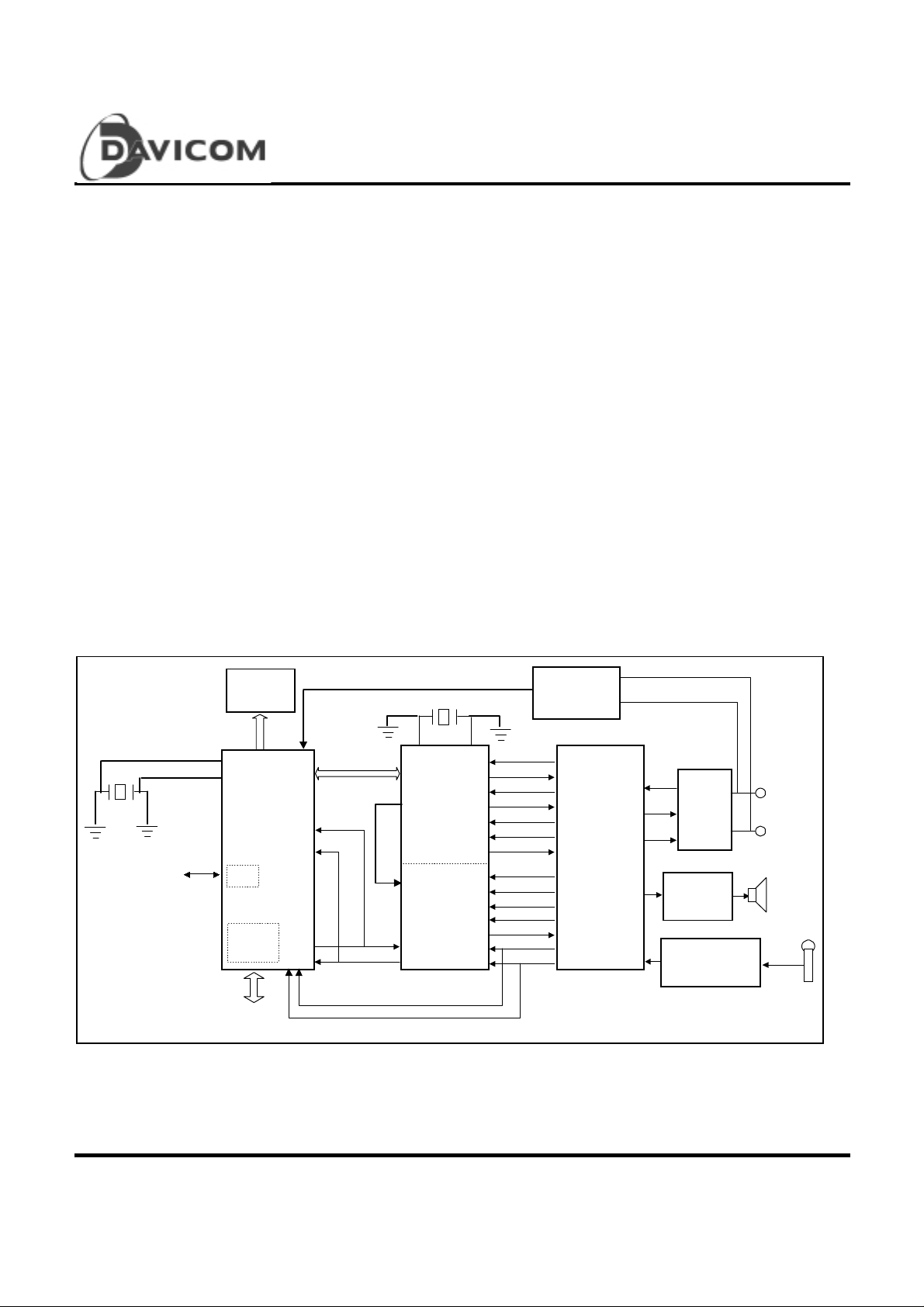
Block Diagram
The DM560P modem reference design is preapproved for FCC part 68 and provides minimum
design cycle time, with minimum cost to insure the
maximum amount of success.
The simplified modem system, show n in figure
below, illustrates the basic interconnection between
the MCU, DSP, AFE and other basic co m ponents of
a modem. The individual elements of the DM560P
are:
• DM6580 Analog Front End (AFE). 28-pin PLCC
package
• DM6581 ITU-T V.90 Transmit Digital Signal
Processor (TX DSP). 100-pin QFP package
• DM6582 ITU-T V.90 Receive Digital Signal
Processor (RX DSP). 100-pin QFP package
• DM6583 Modem Controller (MCU) built in Plug &
Play (PnP). 100-pin QFP package
29.4912
MHz
ISA Bus
LED
DM658
3
Micro
Controller
Unit
PnP
V.24
Interface
V.24
Interface
Address &
Data Bus
MSCLK
TxD
RxD
40.32MHz
DM658
1
TX DSP
DM658
2
RX DSP
Detector
SCLK
DIT
DOT
TFS
DIR
DOR
RFS
TxBCLK
TxSCLK*2
RxBCLK
RxSCLK
20.16MHz
TxDCLK
RxDCLK
Ring
DM658
0
Analog
Front End
SPKR
RxIN
TxA1
DAA
TxA2
Speaker
Driver
Microphone
Driver
Lin
e
Preliminary 1
Version: DM560P -DS-P07
August 11, 2000
Page 2

DM560P
V.90 Integrated Data/Fax/Voice/Speakerphone Modem Device Set
Table of Conten ts
General Descri pti on 1
Block Diagram 1
Features 3
Chipset
Chip 1: DM6583 Modem Controller Unit with PnP
DM6583 Description 4
DM6583 Block Diagram 4
DM6583 Features 4
DM6583 Pin Configuration 5
DM6583 Pin Description 6
DM6583 Functional Description 8
1. Operating Mode Selection 8
2. Micro-controller (8032) Reference 8
3. Micro-c ontroller Register Description 8
4. UART (16550A) Emulation Registers 9
5. Plug and Play (PnP) Module 16
DM6583 Absolute Maximum Ratings 24
DM6583 Electrical Characteristics 24
DM6583 Timing Diagrams 25
Chip 2: DM6581 ITU-T V.90 TX DSP
Chip 3: DM6582 ITU-T V.90 RX DSP
DM6581/82 Description 26
DM6581/82 Block Diagram 26
DM6581/82 Features 26
DM6581/82 Pin Configuration 27
DM6581/82 Pin Description 28
DM6581/82 Functional Description 29
1. System Cloc k 29
2. Serial Port 29
3. Dual Port RAM 30
4. Interrupt 30
DM6581/82 Absolute Maximum Ratings 31
DM6581/82 Electrical Characteristics 31
DM6581/82 Timing Diagrams 32
Chip 3: DM6580 Analog Front End
DM6580 Description 33
DM6580 Block Diagram 33
DM6580 Features 34
DM6580 Pin Configuration 34
DM6580 Pin Description 35
DM6580 Functional Description 35
DM6580 Absolute Maximum Ratings 37
DM6580 DC Characteristics 37
DM6580 AC Characteristics & Timing Diagrams 37
DM6580 Performance 37
Package Information 38
Ordering Information 40
Company Overview 40
Contacts 40
Appendix A-1 Internal Card Application Circuit 41
Appendix A-2 Internal Card Reference B.O.M. 42
Appendix B Copy Of FCC Approval Certificate 43
2 Preliminary
Version: DM560P -DS-P07
August 11, 2000
Page 3

Features
DM560P
V.90 Integrated Data/Fax/Voice/Speakerphone Modem Device Set
Set
■ Compatibility
- ITU-T V.90 (56000 to 28000 bps)
- ITU-T V.34 (33600 to 2400 bps)
- CCITT V.32bis (14400, 12000, 9600, 7200,
4800bps)
- CCITT V.32 (9600, 7200, 4800bps)
- CCITT V.22bis (2400, 1200bps)
- CCITT V.22 (1200bps)
- CCITT V.23 (1200/75bps)
- Bell 212A (1200bps)
- Bell 103 (300bps)
■ Fax
- CCITT V.17 (14400, 12000, 7200bps)
- CCITT V.29 (9600, 7200bps)
- CCITT V.27ter (4800, 2400bps)
- CCITT V.21 Channel 2 (300bps)
- Group III, Class 1
■■■■ Data Error Correction
- MNP Class 4
- CCITT V.42 LAPM
■ Data Compression
- MNP Class5
- CCITT V.42bis
■ Voice compression
- 2 and 4 bit ADPCM
- IMA ADPCM (Developing)
- 8 Bit PCM
■ DTE Interface
- DTE speed up to 115200bps
■ Enhanced T” command set and S registers
- TIA/EIA 578 Fax Class 1 command set
- TIA/EIA IS-101 Voice command set
■ Video-ready modem interface V.80(Developing)
■ V.8bis (Developing)
■ Integrated UART 16550
■ Parallel and Serial interfaces
- 6, 7 and 8 bit character support
- Even, odd, mark and none parity detection and
generation
- 1 and 2 stop bit support
- Auto DTE data speed detection through “AT”
■ Caller identification (Caller ID) support
■ Speakerphone
■ Selectable world wide call progress tone detection
■ 16 Bit over-sampling codec
■ Compromise and adaptive equalizer providing
channel impairment compensation
■ Plug and Play (PnP) support
■ Enhanced 8032 compatible mi cro-c o ntroll e r
■ Power Management (power down mode)
■ 8 selectable interrupts
■ Access up to 256K bytes external program
memory
■ Access up to 64K bytes external data memory
■ NVRAM to store two user configurable, selectable
profiles with three programmable telephone
numbers
■ Full duplex data mode test capabilities
- Analog loop test
- TIA/EIA 602, ITU V.25 ter AT command
Chipset
The DM560P integrated modem device set contains 4 VLSI devices as described below:
1. DM6583 Modem Controller Unit with PnP for ISA
2. DM6580 Analog Front End (AFE)
3. DM6581 ITU-T V.90 Transmit Digital Signal Processor (TX DSP)
4. DM6582 ITU-T V.90 Receive Digital Signal Processor (RX DSP)
Preliminary 3
Version: DM560P -DS-P07
August 11, 2000
Page 4
V.90 Integrated Data/Fax/Voice/Speakerphone Modem Device Set
Chip 1: Modem Controller Unit with Pn P for ISA
DM6583 Description
The DM6583 Modem Control Unit is designed for
use in high speed internal and external modem
applicati ons. The DM6583 interface is compatible
with the DM6581/DM6582 Transmit and Receive
Digital Signal Processors. The DM6583 incorporates
a 80C32 micro-controller, a virtual 16550A UART
with FIFO mode, and Plug & Play control logic.
DM6583 Block Diagram
PC Data Bus
PC Address Bus
IRQ & R/W Control
PnP Control
Logic
Virtual 16550
UART
DM560P
The DM6583 MCU performs general modem control
functions, and is also designed to provide Plug and
Play capability for ISA bus systems. The Plug and
Play logic supports software or automatic Plug and
Play selectable I/Os to allow users to configure the
internal modem card without jumpers.
Mode Selection
8032
Micro-Controller
External ROM,
RAM Interface
RS 232 Interface
DM6583 Features
• Control interface support
• Supports parallel and serial interfaces
• Includes a 80C32 micro-controller
• 256K bytes maximum external program memory
• 64K bytes maximum external data memory
• Provides automatic Plug and Play or software
configuration capabilities
• 8 selectable Interrupts
I/O Control Logic
• Conflict free I/O base address selection
• Virtual 16550A UART compatible parallel
interface
• Fully programmable serial interface:
- 6, 7 or 8-bit characters
- Even, odd, mark and none parity bit generation
and detection
- 1 and 2 stop bit generation
- Baud rate generation
- Includes I/O control logic for modem control
interface
Modem Control
Interface
4 Preliminary
Version: DM560P -DS-P07
August 11, 2000
Page 5
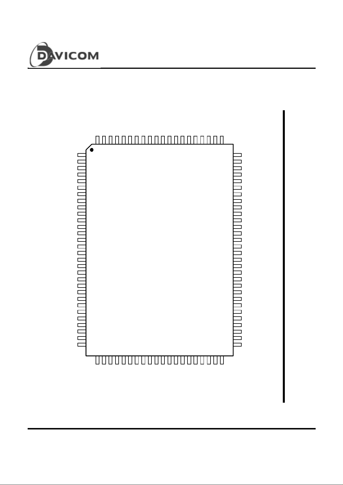
DM6583 Pin Configuration
DM560P
V.90 Integrated Data/Fax/Voice/Speakerphone Modem Device Set
UD0
UD1
UD2
UD3
UD4
UD5
UD6
UD7
/IOR
GND
/IOW
/AEN
A11
A10
A9
A8
A7
A6
A5
A4
A3
A2
A1
A0
V
DD
IRQ4
IRQ5
IRQ7
IRQ10
RESET
1
2
3
4
5
6
7
8
9
10
11
12
13
14
15
16
17
18
19
20
21
22
23
24
25
26
27
28
29
30
DD
EXT/INTB
V
99
100
32
31
PS1
98
33
GND
/TUCS
96
97
35
34
A12
A13
A14
A15
/PNPEN
91
92
93
94
95
DM6583
39
38
37
36
voice sel2
/POR
Voice Sel1
88
89
90
43
424041
TXRCLK
RXRCLK
86
87
45
44
GND
85
46
D0
84
47
D1
83
48
D2
82
49
D3
81
50
80
79
78
77
76
75
74
73
72
71
70
69
68
67
66
65
64
63
62
61
60
59
58
57
56
55
54
53
52
51
D4
D5
D6
D7
CA0
CA1
CA2
CA3
CA4
CA5
CA6
CA7
GND
CA8
CA9
CA10
CA11
CA12
CA13
CA14
CA15
IRQ3
/RD
/WR
/PSEN
ALE/P
TXD
RXD
V
DD
/LCS
XTAL2
XTAL1
IRQ12
IRQ11
DD
V
IRQ15
/PWR
CA17
CA16
/RUCS
GND
T0
T1
/RI
/DTR
/OH
/VOICE
EEPROM1
EEROM3
EEPROM2
Preliminary 5
Version: DM560P -DS-P07
August 11, 2000
Page 6

V.90 Integrated Data/Fax/Voice/Speakerphone Modem Device Set
DM6583 Pin Description
Pin No. Pin Name I/O Description
1 - 8 UD0 - UD7 I/O Data Bus Signal, for internal modem:
These signals are connected to the data bus of the PC I/O. They are
used to transfer data between the PC and the DM6583.
Modem Control Output, for external modem:
Memory address mapping of the contr oller is E800H.
9 /IOR I I/O Rea d:
An act ive lo w input signal used to read data from the DM6583.
10, 41, 68,
85, 96
11 /IOW I I/O Writ e :
12 /AEN I Address Enable:
13 - 24 A11 - A0 I System Address:
25, 36, 52,
100
26, 27, 28,
29, 33, 34,
35, 59
30 RESET I Reset:
31 XTAL1 I Cryst al Oscillator Input
32 XTAL2 O Crystal Oscillator Output
37 /PWR O Controller P rogram Write Enable:
51 /LCS I Loop Current Detection. Modem Input Control:
39 /RUCS O RX DSP Register Select Output:
40,38 CA16,CA17 O Bank Switch Control:
42 T0 I Controller Counter 0 Input
GND P Ground
An act ive lo w input signal used to write data to the DM6583.
This is an active low signal to enable the system address for
DM6583.
These signals are connected to the bus of PC I/O. They are used to
select DM6583 I/O ports.
A0~A7:Modem Control Input for external modem. Memory address
mapping of the controller is E800H.
VDD P +5V Power Supply
IRQ4, IRQ5,
IRQ7, IRQ10,
IRQ11, IRQ12,
IRQ15, IRQ3
O Interrupt Request:
These are the interrupt request pins. Only one pin, which is
decoded from Configuration Register can be active. The active pin
will go high when an interrupt request is generated from the
DM6583.
An active high signal used to reset the DM6583.
This pin is used to enable FLASH ROM programming. In
conf igurations with no FLASH memory, this pin is not connected.
This pin is mapped to bit0 of address D000H.
Memory address mapping of the contr oller is E400H.
These signals are used to switch external program memory
between banks.
CA16 CA17
Bank 0 0 0
Bank 1 1 0
Bank 2 0 1
Bank 3 1 1
DM560P
6 Preliminary
Version: DM560P -DS-P07
August 11, 2000
Page 7
DM560P
V.90 Integrated Data/Fax/Voice/Speakerphone Modem Device Set
DM6583 Pin Description
Pin No. Pin Name I/O Description
43 T1 I Controller Counter 1 Input
44 /RI I Ring Signal Input
45 /DTR I DTR Input Pin (P1.1)
46 /OH O Hook Relay Control (P1.2)
47 /VOICE O Voice Relay Control. Modem Control Output (memory map is bit
48-50 EEPROM 1-3 I/O EEPROM Control Pins (P1.4-P1.6)
53 RXD I Controller Serial Port Data Input
54 TXD O Controller Serial P ort Data Output
55 ALE/P O Controller Address Latch Enable:
56 /PSEN O Controller Program Store Ena ble:
57 /WR O Controller External Data Memory Write Contro l
58 /RD O Controller External Dat a Memory Read Control
60 - 67 CA15 - CA8 O Controller Address Bus
69 - 76 CA7 - CA0 O Controller Address Bus
77 - 84 D7 - D0 I/O Controller Data Bus
86 TXRCLK I Transmitter Baud Rate Clock Input (Controller INT 0)
87 RXRCLK I Receiver Baud Rate Clock Input (Controll er INT 1)
88 /POR O DSP Reset Output
89, 90 VOICE Se1 1
VOICE Se1 2
91 - 94 A12 - A15 I System Address:
95 /PNPEN I PnP Mode Enable:
97 /TUCS O TX DSP Register Select Output:
98 PS1 O Modem Control Port Select Output:
99 EXT/INTB I Select Pin: Used to select internal or external operation.
(continued)
3 of DAA)
Output pulse for latching the low byte of the address during
accesses to the extern al memory.
This output goes low during a fetch from external program memory.
O Modem C o ntro l Out put (Memory map is bit 1-2 of DAA at memory
address D000H)
These signals are connected to the bus of the PC I/O. They are
used to select the DM6583 I/O ports.
This pin selects PnP mode. When connected to ground, the
DM6583 will enter PnP mode when it receives the PnP initiation key
sequence. When disconnected, an internal pull up will disable the
Plug and Play function.
Memory address mapping of the contr oller is F000H.
Memory address mapping of the contr oller is D800H.
0: internal modem
1: external modem
Preliminary 7
Version: DM560P -DS-P07
August 11, 2000
Page 8

DM560P
V.90 Integrated Data/Fax/Voice/Speakerphone Modem Device Set
DM6583 Functional Description
1. Operating Mode Selection
The DM6583 MCU can be used in both internal and
external modem applications. When operating as an
internal modem, the EXT/INTB input (pin 99) must
be attached to ground. When the DM6583 is
operating as an external modem, the EXT/INTB
input (pin 99) must attached to VDD.
2. Micro-controller Program Memory
The DM6583 supports two bank switch control pins
to switch external program memory among four
banks. The DM6583 can access a total of 256K of
external pr ogram mem ory.
Address mappi ng:
bank0: 00000H - 0FFFFH
bank1: 10000H - 1FFFFH
bank2: 20000H - 2FFFFH
bank3: 30000H - 3FFFFH
For bank switching, three instruc tions must be
included in software.
Switch to bank1:
CLR P1.3
SETB P1.7
JMP BANK 1 ADDRESS
Switch to bank2:
CLR P1.7
SETB P1.3
JMP BANK 2 ADDRESS
Micro-contro ller Power Down Mode
An instruction that sets the register PD (PCON.1) will
cause the 80C32 to enter power down mode. There
are three ways to wake up the 80C32
(1) Positive pulse signal occurring at the reset pin of
the 80C32
(2) Negative pulse occurring at / R I (P1.0) of the
80C32
(3) Programming the PnP Wake Up Controller
Register.
Enhanced Internal direct Memory
There are two 128 byte banks of intern al direc t
memory in the 80C32. The system uses the lower
128 bytes under normal conditions. Switching to the
upper bank is achieved by loading register 8FH.1
(SFR of the 80C32) with 1. Switching to the lower
bank can be achieved by loading the same register
with 0.
Reflash Program Memory
By setting 8F.2H the system can switch program and
data memory. If the system uses FLASH memory as
program memory this function is used to reflash
program code by downloading the program to data
memory then switching them.
Example:
SETB 8FH.2
LJMP 0000H
Switch to bank3:
CLR P1.7
CLR P1.3
JMP BANK 3 ADDRESS
Return to bank 0:
SETB P1.7
SETB P1.3
JMP BANK 0 ADDRESS
* For detailed information about the micro-controller,
refer to the Programm er's Guid e to 8032.
8 Preliminary
Micro-controller Register Description
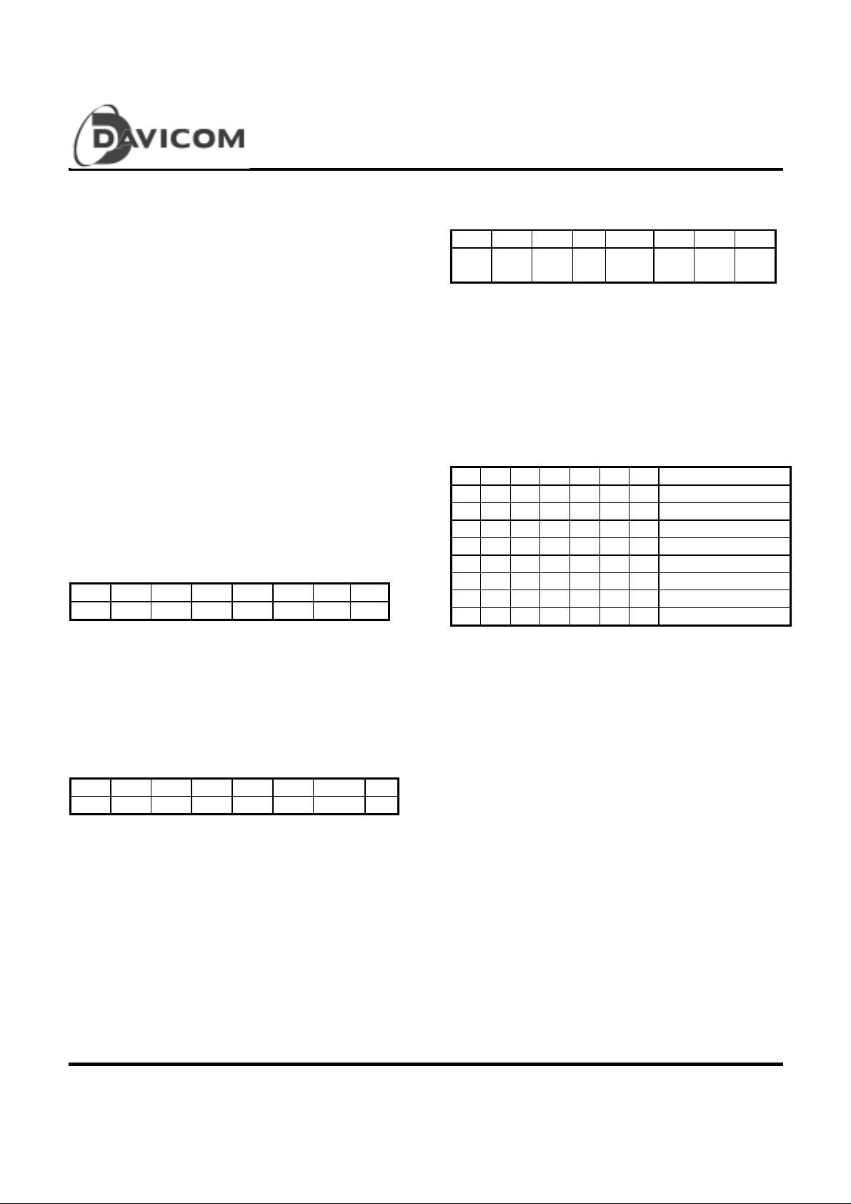
UART Clock Register:
Address D4000H Reset State: 06H
Write Only
bit7 bit6 bit5 bit4 bit3 bit2 Bit1 bit0
X dat6 dat5 dat4 dat3 dat2 dat1 0
Version: DM560P -DS-P07
August 11, 2000
Page 9
DM560P
V.90 Integrated Data/Fax/Voice/Speakerphone Modem Device Set
UART Clock
The internal clock of the virtual UART logic is fixed at
1.8432MHz. The clock is derived from the MSCLK
signal from the DM6582 DSP, or an external 30Mhz
crystal. The UART 1.8432MHz clock will be obtained
by division. When the operating frequency of the
DM6583 controller changes, the divider should be
changed accordingly. This divider is specif ie d by the
Configuration Register which can be written by the
DM6583 controller. The address mapping of the
register is D400H: ( DM 6583 controller memory
mapping)
Bit 0: Always 0.
Bit 6-1 : define the cloc k divider range from 2 to 64
(even number).
Bit 7: Not used.
UART Baud Generator Divisor Latch Register:
Address EC00H
Read only
bit7 bit6 bit5 bit4 bit3 bit2 bit1 bit0
dat7 dat6 dat5 dat4 dat3 dat2 dat1 dat0
Modem Output Port Regi st er: Address D000H
Write only
bit7 bit6 bit5 bit4 bit3 bit2 bit1 bit0
/Voice Voice
These 4 bits control the DM6583 output ports.
PnP Isolation & Resource Data Port: Address
F800H
Write only
The PnP isolation and resource data can be bytesequentially written to the corresponding memory
through this register.
Auto-configuration Register: Address F400H
bit2 bit1 bit0 IRQ bit5 bit4 bit3 I/O
0 0 0 3 0 0 0 03F8-03FF(COM1)
0 0 1 4 0 0 1 02F8-02FF(COM2)
0 1 0 5 0 1 0 03E8-03EF(COM3)
0 1 1 7 0 1 1 02E8-02EF(COM4)
1 0 0 10 1 0 0 03F0-03F7(COM5)
1 0 1 11 1 0 1 02F0-02F7(COM6)
1 1 0 12 1 1 0 03E0-03E7(COM7)
1 1 1 15 1 1 1 02E0-02E7(COM8)
-sel2
Voice
-Sel1
/POR
By reading this register, the micro-controller can
monitor the value of the low byte divisor latch of the
virtual UART baud generator (see DLL in next
section) and determine the baud rate clock itself.
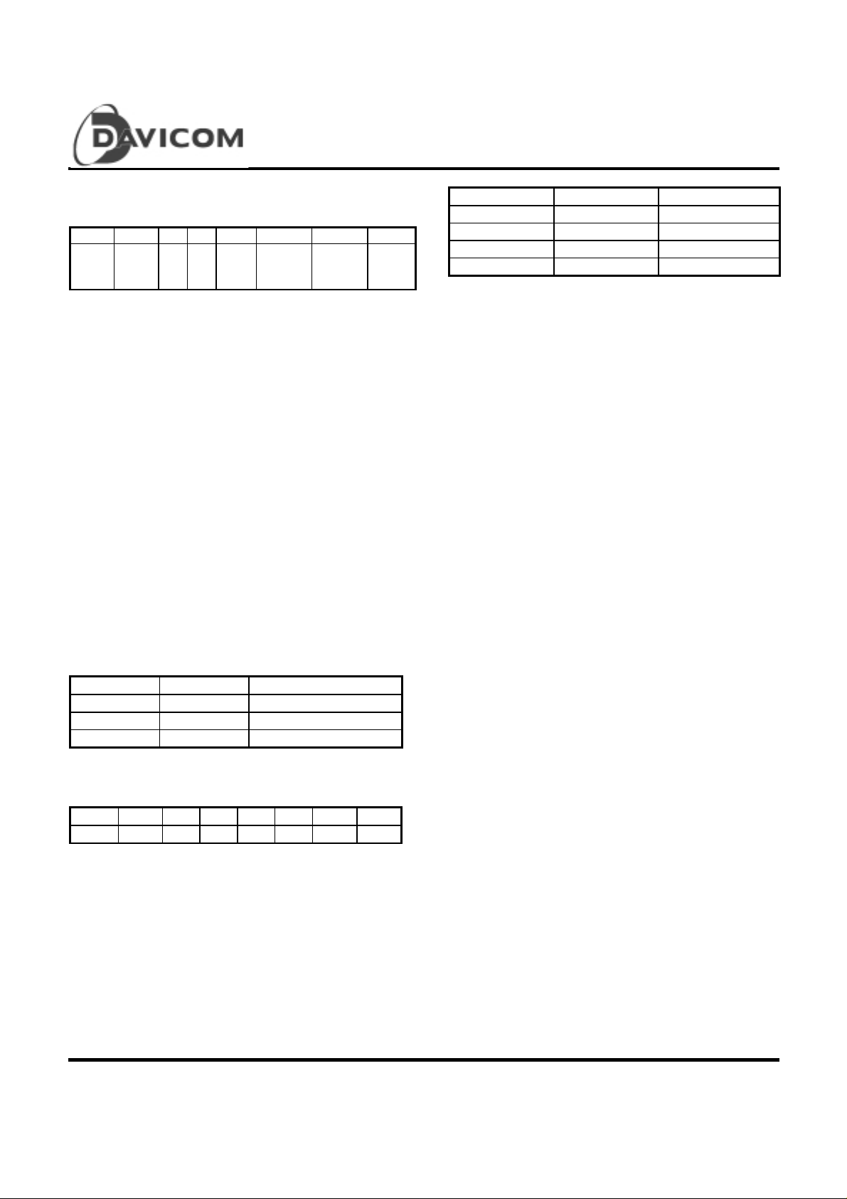
Modem Status Control Register (MSCR):
Address E000H
Write only
bit7 bit6 bit5 bit4 bit3 bit2 bit1 bit0
0000/CTS/DSR/DCD/RI
This register contains information about the line
status of the modem. The available signals are Ring
Detect (/RI), Carrier Detect (/DCD) , Data Set Ready
(/DSR) and Clear To Send (/CTS).
The default I/O base and IRQ data stored in 93C46 is
loaded to this register by the micro-controller. The
micro-controller can also get the current I/O base
and IRQ information settings by performing a read
from this register. The configuration determined by
this register will be disabled when the register
detects the Initiation Key described in the next
section.
Bit 6: This bit is set to inform micro-controller that the
current I/O base and IRQ data should be stored to
93C46 as the default setting for the next power-on
reset through programming the Auto-configuration
Register. This bit will be cleared by micro-controller.
Bit 7: When bit 7 is set, it enables the hardware
configuration to be set according to bit 0-bit 5
(Jumperless mode) and loads the proper value into
the PnP Registers including I/O and Interrupt
Configuration Registers. This bit will be reset, when it
receives PnP Initiation Key sequence.
Preliminary 9
Version: DM560P -DS-P07
August 11, 2000
Page 10

V.90 Integrated Data/Fax/Voice/Speakerphone Modem Device Set
Auto-configuration Register: Address F400H
(continued)
* When a reset condition occurs, the I/O and
Interrupt configuration registers must be reset to the
default value according to bit 0 - bit 5.
RxDataBits Register: Address DC00H
Write only
Once the RxDataBit set to 1, the data in the RxBuffer
will be transferred to RxFiFo. The transfer bit number
is the same as the programming valu e of RxDataBits
Register.
RxBuffer: Address DC01H
Write only
Receive data will be written to the RxBuffer and will
be input to the RxHDLC circuit. The RxBuffer is 16
bytes wide.
RxFiFo: Address DC01H
Read only
After the data has been passed from the RxBuffer to
the RxHDLC circuit, the RxHDLC circuit will remove
the 7eH patterns and transfer the results to the
RxFiFo. There RxFiFo is 21 bytes wide.
TxDataBits Register: Address DC02H
Write only
Data written to TxDataBits will be presented to the
TxFiFo. The data in TxFiFo will be transferred to
TXHDLC circuit. The transfer bit number is the same
as the value of TxDataBit s register. If the TxFiFo is
empty, a 7e pattern will be loaded to the TxFiFo. If
TxFiFo is not empt y and the data frame has the
pattern of five consecutive “1” , then the TXHDLC
circuit will insert “0” automatically.
TxFiFo Register: Address DC03H
Write only
The o riginal HDLC frame data will be loaded to the
TxFiFo, presented to the input of the TxHDLC circuit.
The TxFiFo is 21 bytes wide.
TxBuffer: Address DC03H
Read only
According to TxDataBits, the TxHDLC circuit will
transfer the same number data bits to the TxBuffer.
The TxBuffer i s 16 bytes wide.
DM560P
HDLC CNTL/STATUS Register: Address DC04H
Bit0: TxReady0
0: indicates the data in the TxFiFo has deceased
to zero and the HDLC circuit has transferred
st
7eH pattern.
the 1
1: indicates that the TxFiFo data is greater than or
equal to the threshold value.
Bit1: Rxdata
0: all the data in the RxBuffer has been read.
1: Programed by software to indicate that all data
in the RxDataBits register has been written to
the RxBuffer.
Bit2: TxF i Fo Thr e shold
0: TxFiFo threshold No. = 11
1: TxFiFo threshold No. = 16
Bit3: TxFiFo Status
0: data No. in TxFiFo >= threshold
1: data No. in TxFiFo <= threshold
Bit4: Txda ta
0: A write action to TxDataBites register will clear
this bit.
1: Bit No. in TxBuffer = TxDataBits register.
Bit5: RxFiFo empty
0: data bytes No. in RxFiFo <>0
1: data bytes No. in RxFiFo = 0
Bit6: Reset
0: Normal state
1: reset HDLC circuit
In____ buffer register: Address DC08
writ e only
Controller write the original data to this temp buffer.
Out ____ buffer register: Address DC08H
read only
Controller read the result data from this buffer
Status/Rst register: Address DC09H
Bit0: data ready f lag (read only)
1: data has been load to out _ buffer. (clear
automatically by a read from out_ buffer)
0: data hasn’t been load to out _ buffer.
Bit1: frame end flag (read only)
1: Indicate end of HDLC frame (clear by a reset
action)
Bit2: fram ready flag (read only)
1: CRC check ok.
0: CRC check fail.
Bit3: In _ buffer empty flag
10 Preliminary
Version: DM560P -DS-P07
August 11, 2000
Page 11

V.90 Integrated Data/Fax/Voice/Speakerphone Modem Device Set
1: In _ buffer empty (clear automatically by a
write to In _buffer)
0: In _ buffer not empty
Bit7: reset bit(write only)
1: software reset
(4)CRCL register: Address DC0AH (read only)
(5)CRCH register: Address DC0BH (read only)
UART (16550A) Emulation Regist ers
Receiver Buffer (Read), Transmitter Holding
Register (Write): Address: 0 (DLAB=0)
Reset State 00h
bit7 bit6 bit5 bit4 bit3 Bit2 bit1 bit0
dat7 dat6 dat5 dat4 dat3 Dat2 dat1 dat0
When this register address is read, it contai ns the
parallel received data. Data to be transmitted is
written to this registe r .
Interrupt Enable Register (IER): Address 1
DM560P
Interrupt Identification Register (IIR): Address 2
Reset State 01h, Read only
Bit7 Bit6 bit5 bit4 bit3 bit2 bit1 bit0
FIFO
Enable
In order to provide minimum software overhead
during data transfers, the virtual UART prioritizes
interrupt s into four levels as follows: Receiver Line
Status (priority 1), Receiver Data Available (priority
2), Character Timeout Indi cation (priority 2, FIFO
mode only), Transmitter Holding Register Empty
(priorit y 3), and Modem Status (priority 4).
The IIR register gives pri ori tized information
regarding the status of i nterrupt conditions. W hen
accessed, the IIR indic ates the highest priority
interrupt that is pending.
000D3:
INTD2
D2:
INTD1
D1:
INTD0
D0:
int
Pending
Reset State 00h, Write Only
bit7 bit6 bit5Bit4 bit3 bit2 bit1 bit0
0 0 0 0 Enable
Modem
Status
Intr
Enable
Line
Status
Intr
Enable
TX
Holding
Registe
r
Intr
Enable
RX
Data
Intr
This 8-bit register enables the four types of interrupts
as described below. Each interrupt source can
activate the INT output signal if enabled by this
register. Resetting bits 0 through 3 will disable all
UART interrupts.
Bit 0: This bit enables the Received Data Avail able
and timeout interrupts in the FIFO mode when
set to logic 1.
Bit 1: This bit enables the Transmitter Holding
Register Empty Interrupt when set to logic 1.
Bit 2: This bit enables the Receiver Line Status
Interrupt when set to logic 1.
Bit 3: T his bit enables the MODEM Status Interrupt
when set to logic 1.
Bit 0: Thi s bit c an be used in either a prioritized
interrupt or polled environment to indicate
whether an interrupt is pending. When this bit
is a logic 0, an interrupt is pending, and the IIR
contents may be used as a pointer to the
appropriate interrupt service routine. When bit
0 is a logic 1, no int er r upt is pending, and
polling (if used) continues.
Bit 1-2: The se tw o bit s of the IIR are used to identify
the highest priority interrupt pending, as
indicated in the table below.
Bit 3: In character mode, this bit is 0. In FIFO mode,
this bit is set, along with bit 2, when a timeout
interrupt is pending.
Bit 4-6: Not used
Bit 7: FIFO always enabled.
Bit 4-7: Not used
Preliminary 11
Version: DM560P -DS-P07
August 11, 2000
Page 12

DM560P
V.90 Integrated Data/Fax/Voice/Speakerphone Modem Device Set
Interrupt Identification Register (IIR): Address 2 (continued)
D3 D2 D1 D0 Priority Level Interrupt Type Condition Reset
0001- - - 0 1 1 0 Highest Receiver Line
Status
0 1 0 0 Second Receiver Data
Available
1 1 0 0 Second Character Timeout
Indication
0 0 1 0 Third Transmitter
Holding Register
Empty
0 0 0 0 Fourt h Modem Status Cl ear to Send, Data Set
Overrun Error, Pari ty E rro r,
Framing Error or Break
Interrupt
Receiver Data Available or
Trigger Lev el Reached
No characters have been
read from or written to the
Rx FIFO during
programming time interval,
and the Rx FIFO is not
empty
Ready to accept new data
for transmi ssion
Ready, Ring Indi c ator or
Data Carrier Detected
Reads the Line Status
Register
Reads the Receiver Buff er
Register or the F IFO has
Dropped Below the
threshold value
Reads The Receiver Buff er
Register
Reads the IIR Register or (if
source of interrupt) W rites
To The Transmitter Holding
Register
Reads the Modem Status
Register
12 Preliminary
Version: DM560P -DS-P07
August 11, 2000
Page 13
DM560P
V.90 Integrated Data/Fax/Voice/Speakerphone Modem Device Set
FIFO Control Register (FCR): Address 2
Reset State 00h , write only
bit7 bit6 bit5 bit4 bit3 bit2 bit1 bit0
RCVR
(MSB)
Trig
RCVR
Trig
(LSB)
00DMA
Mode
TxFIFO
Reset
RxFIFO
Reset
FIFO
Enable
This is a write only register at the same location as
the IIR, which is a read only register. This register is
used to enable the FIFOs, clear the FIFOs, set the
RxFIFO trigger level, and select the type of DMA
signal.
Bit 0: FIFO Enable, This bit is always high
Bit 1: Writing a 1 to FCR1 clears all bytes in the
RxFIFO and resets the counter logic to 0.
Bit 2: Writing a 1 to FCR2 clears all bytes in the
TxFIFO and resets the counter l ogic t o 0.
Bit 3: Setting FCR3 to 1 will cause the RXRDY and
TXRDY pins to change from mode 0 to mode 1
if FCR0 = 1.
Bit 4-5: Reserved
Bit 6-7: FCR6, FCR7 are used to set the trigger level
for the RxFIFO i nterrupt.
WLS1 WLS0 Word Length
005 bits
016 bits
107 bits
118 bits
Bit 0-1: WLS0-1 specifies the number of bits in each
transmitted and received serial character.
Bit 2: STB specifies the numbe r of sto p bits in each
transmitted character. If bit 2 is a logic 0, one
sto p bit is generated in the transmitted data. If
bit 2 is a logic 1 when a 5-bit word length is
selected via bits 0 and 1, one and a half stops
are generated. If bit 2 is a logic 1 when either a
6-, 7- or 8-bit word length is selected, two stop
bits are generated. The Receiver checks the
first Stop-bit only, regardless of the number of
Stop bits selected.
Bit 3: Logic 1 indicates that the PC has enabled
parity generation and checking.
Bit 4: Logic 1 indicates that the PC is requesting an
even number of logic 1s (even parity
generation) to be transmitted or checked.
Logic 0 indicates that the PC is requesting odd
parity generation and checking.
FCR6 FCR7 RxFIFO Trigger Level
00 01
01 04
10 08
Line Control Register (LCR): Address 3
Reset State 00h, Write Only
bit7 bit6 bit5 bit4 bit3 bit2 bit1 bit0
DLAB SBRK STP EPS PEN STB WLS1 WLS0
This register is available to maintain compatibility
with the standard 16550 register set, and provides
information to the internal hardware that is used to
determine the number of bits per character.
Preliminary 13
Version: DM560P -DS-P07
August 11, 2000
Bit 5: When bits 3, 4 and 5 are logic 1, the parity bit
is transmitted and checked by the receiver as
logic 0. If bits 3 and 5 are 1 and bit 4 is lo g ic 0,
then the parity is transmitted and checked as
logic 1.
Bit 6: This is a Break Control bit. When it is set to
logic 1, a break condition is indicated.
Bit 7: The Divisor Latch Access bit must be set to
logic 1 to access the Divisor Latches of the
baud generator during a read or write
operation. It must be set to logic 0 to access
the Receiver Buffer, the Transmitter Holding
Register, or t he Interrupt Enable Register.
Page 14

DM560P
V.90 Integrated Data/Fax/Voice/Speakerphone Modem Device Set
Modem Control Register (MCR) : Address 4
Reset State 00h
bit7 bit6 bit5 bit4 bit3 bit2 bit1 bit0
000000RTSDTR
Bit 0: T his bit asserts a Data Terminal Ready
condition that is readable via port P1.1 of the microcontroller 80C32. When bit 0 is set to logic 1, the P1.1
is forced to logic 0. When bit 0 is reset to logic 0, the
P1.1 is forced to logic 1.
Bit 1: This bit asserts a Request To Send condition
that is readable via port P3.4 of the micro- c ontroller
80C32. When bit 1 is set to logic 1, the P3.4 is forced
to logic 0. When bit 1 is reset to logic 0, the P3.4 is
forced to logic 1.
Line Status Register (LSR): Address 5
Reset State 60h, Read only
bit7 bit6 bit5 bit4 bit3 bit2 bit1 bit0
RCV ETEMT THRE BI FE PE OE DR
This register prov ides status i nformation to the host
PC concerning character transf er . Bit 1- 4 indic ates
error conditi ons that produce a Receiver Line Status
interrupt whenever any of the corresponding
conditions are detected. The Line Status Register is
valid for read operations only.
Bit 0: Set to logic 1 when a received character is
available in the RxFIFO. This bit is reset to logic 0
when the RxFIFO is empty.
Bit 1: An Overrun error will occur only after the
RxFIFO is full and the next character has over written
the unread FIFO data. This bit is reset upon reading
the Line Status Register.
Bit 3: This bit is the Framing Error (FE) indicator. Bit 3
indicates that the received character did not have a
valid stop bit. Bit 3 is set to a logic 1 whenever the stop
bit following the last data bit or parity bit is detected as
a zero bit (spacing level). The FE bit is reset whenever
the CPU reads the contents of the Line Status
Register. The FE error condition is associated with the
particular character in the FIFO to which it applies.
This error is revealed to the CPU when its associated
character i s at the top of the FIFO.
Bit 4: T his bit is a Break Interr upt (BI) indicator. Bit 4
is set to logi c 1 whenever t he received data input is
held in the Spacing (logic 0) state for longer than a full
word transmission time (tha t is, the total time of Start
bit + data bits + Parity + Stop bits). The BI indicator is
reset whenever the CPU reads the content s of the
Line Status Register. The BI error condition is
associated with the particular character in the FIFO to
which it applies. This error is revealed to the CPU
when its associated character is at the top of the FIFO.
Bit 5: This bit is a Transmitter Holding Register Empty
indicator. Bit 5 indicates that UART is ready t o accept
a new character for transmissio n. In addition, thi s bit
causes the UART to issue an interrupt to the CPU
when the Transmit Holding Register Empty Interrupt
Enable is set high. The THRE bit is reset to logic 0
when the host CPU loads a character into the
Transmit Holding register. In the FIFO mode, this bit is
set when the TxFIFO is empty, and is cleared when at
least 1 byte is written to the TxFIFO.
Bit 6: T his bit is the Transmitter Empty indicator. Bit 6
is set to a logic 1 whenever the Transmitter Holding
Register (THR) is empty, and is reset to a logic 0
whenever the THR cont ains a charact er . In FIFO
mode, this bit is set to 1 whenever the transmit FIFO is
empty.
Bit 2: A logic 1 indicates that a received character
does not have the correct even or odd parity as
selected by the Parity Select bit. This error is set when
the corresponding character is at the top of the
RxFIFO. It will remain set until the CPU reads the
LSR.
14 Preliminary
Bit 7: In character mode, this bit is 0. In FIFO mode,
this bit is set when there is at least one parity error,
framing error, or break indication in the FIFO. If there
are no subsequent errors in the FIFO, LSR7 is cleared
when the CPU reads the LSR.
Version: DM560P -DS-P07
August 11, 2000
Page 15

V.90 Integrated Data/Fax/Voice/Speakerphone Modem Device Set
Modem Status Regi st er (MS R) : Address 6
Reset State bit 0-3 : low , bit 4-7: Input Signal
bit7 bit6 bit5 bit4 bit3 bit2 bit1 bit0
DCD RI DSR CTS DDCD TERI DDSR DCTS
This 8-bit register prov ides the current state of the
control lines from the Modem to the CPU. In addition,
four bits of the Modem Status Register provide change
information. These bits are set to a logic 1 w henever a
control input from the Modem changes state. They are
reset to logic 0 whenever the CPU reads the Modem
Status Register.
Bit 0: This bit is the Delta Clear to Send (DCTS)
indicator. B i t 0 indicates that the CTS (MSR Bit 4) has
changed state since the last time it was read by the
CPU.
Bit 1: T his bit is the Delta Data Set Ready (DDSR)
indicator. B it 1 indicates that the DSR (MSR Bit 5) has
changed state since the last time it was read by the
CPU.
Bit 2: This bit is the Trailing Edge of Ring indicator. Bit
2 indicates that the RI (MSR Bit 6) has changed from a
low to a high state.
Bit 3: This bit is the Delta Data Carrier Detect (DDCD)
indicator. B it 3 indicates that the DCD (MSR Bti 7) has
changed state.
Note: Whenever bit 0, 1, 2 or 3 is set to a logic 1, a
Modem Status Interrupt is generated.
Bit 4: This bit reflects the value of MSR Bit 4 (CTS).
Bit 5: This bit reflects the value of MSR Bit 5 (DSR).
Bit 6: This bit reflects the value of MSR Bit 6 (RI).
Bit 7: This bit reflects the value of MSR Bit 7 (DCD).
DM560P
Scratch Regist er (SCR): Address 7
Reset State 00h
This 8-bit Read/Wri te Register does not control the
UART in any way. It is intended as a Scratch Pad
Register to be used by the programmer to hold data
temporarily.
Divisor Latch (DLL): Address 0 (DLA B = 1)
Reset State 00h
bit7 bit6 bit5 bit4 bit3 bit2 bit1 bit0
DAT7 DAT6 DAT5 DAT4 DAT3 DAT2 DAT1 DAT0
This register contains baud rate information from the
host PC. The PC sets the Divisor Latch Register
values.
Divisor Latch (DLM): Address 1 (DLAB = 1)
Reset State 00h
bit7 bit6 bit5 bit4 bit3 bit2 bit1 bit0
DAT7 DAT6 DAT5 DAT4 DAT3 DAT2 DAT1 DAT0
This register contains baud rate information from the
host PC.
Note: Two 8-bit latches (DLL-DLM) store the divisor in
16-digit binary format. The desired baud rate can be
obtained by dividing the 115200Hz clock by the
divisor.
Desired
Baud Rate
50 2304
75 1536
110 1047
150 768
300 384
600 192
1200 96
2400 48
4800 24
9600 12
19200 6
38400 3
57600 2
115200 1
Divisor
Value
Preliminary 15
Version: DM560P -DS-P07
August 11, 2000
Page 16

V.90 Integrated Data/Fax/Voice/Speakerphone Modem Device Set
Plug and Play (PnP) Module
Auto-c onfigura t i on Ports
Three 8-bit I/O ports are defined for Plug and Play
read/write operations. They are called Autoconfiguration ports as listed below.
Port Type Location
ADDRESS W 0279H
(Printer stat us port )
WRITE_
DATA
READ_
DATA
To access the Plug and Play Register, a host should
follow this procedur e: Write a target register address
(Register Index), choose a port (WRITE_DATA or
READ_DATA), then enter data.
Card Control Registers
W 0A79H
(Print er status port + 0800H)
R Relocatable in range
0203H to 03FFH
DM560P
The Plug and Play Register could be directly accessed
without the need to write to the ADDRESS port before
each access. The ADDESS port is als o t he write
destination of the initiation key, which will be described
later.
Plug and Play Registers
The Plug and Play Registers may be divided into Card
Registers and Logical Device Registers. Ac cording to
the Plug & Play specification, if a PnP card contains
more than one logical device, there are one more
copies of Logical Dev ic e Registers in the PnP card.
However, the DM6583A contains only one logical
device, the Card Register and Logical Device
Registers are unique for each card. Those PnP
registers or bit s not defined below are all read with
value = 0.
Index Name Type Definition
00H S et RD_DATA port W The loc ation of the READ_DATA port is determined by writing to this
register. Bi ts [7:0] become ISA I/O read port address bits [9:2]. Address
bits [1:0] of the READ_DATA port ar e always 1.
01H Serial Isolation R A read to this register causes a PnP card in the Isolation state to compare
one bit of the card serial ID. This process is described in more detail in the
next section.
02H Config Control W
03H Wake [CSN] W A write to this register will cause all cards that have a CSN that matches the
04H Resource Data R A read from this register reads the next byte of resource data. The Status
05H Status R Bit [0], when set, indicates it is ready to read the next data byte from the
06H Card Select Number
(CSN)
Bit [0] - Reset Command Setting
This bit will reset all logic al devices and restore configuration register s to
their power-up values. The CSN is preserved.
Bit [1] - Wait for Key Command Setting
This bit makes the Pn P card return to the Wait for K ey state. The CSN is
preserved.
Bit [2] - PnP Reset CS N Command Sett in g
This bit will reset the card CSN to 0. Note that the hardware will
automatically clear the bits without any need for software to clear them.
write data [7:0] to go from the Sleep state to either the 1) Isolation state if the
write data for this command is zero, or 2) Configuration state if the write
data is not zero.
Register must be pol led un ti l bit[0] is set before this register may be read.
Resource Data Register.
R/W A write to this register sets a card CSN. After a serial identification process,
the CSN value (CSN) is uniquely assigned to each ISA PnP card so that
each card may be individually selected during a Wake[CSN] command.
16 Preliminary
Version: DM560P -DS-P07
August 11, 2000
Page 17

DM560P
V.90 Integrated Data/Fax/Voice/Speakerphone Modem Device Set
Card Control Registers (continued)
Index Name Type Definition
07H Logical Device R 00H (Only one logical device in DM6583A)
Logical Device Control Registers
Index Name Type Definition
30H Activate R/W For each logical device, there is one Activate register that controls whether
or not the device is active on the ISA bus. Bit[0], if set, activates the logical
device. Before a logical device is activated, I/O range check must be
disabled.
31H I/O Range Check R/W This register is used to perform a conflict check on the I/O port range
programmed for use by a logic al d evice.
Bit[1] - This bit, when set, enables I/O range check. I/O port range c he ck is
only valid when the logical device is inactive.
Bit[0] - If set, this bit forces logical device to respond to I/O reads within
logical device assigned I/O range with a 55H when I/O range check is in
operation. If clear, the logical device drives AAH.
Logical Device Configuration Registers
I/O Conf i guration Regist e r s
Index Name Type Definition
60H I/O base address bits[15:8] R/W Read/write value indicating the selected I/O Lower Limit Address Bits
[15:8] for I/O descriptor 0. If a logical device indicates it uses only 10
bits for decoding, then bits [15:10] need not to be supported.
61H I/O base address bits[7:3] R/W Read/write value indicating the selected I/O Lower Input Address Bits
[7:3] for I/O descriptor 0.
Interrupt Configuration Registers
Index Name Type Definition
70H IRQ level R/W Read/write value indicating a selected Interrupt Level Bits[3:0] Select which
ISA interrupt level is used. A value of 1 selects IRQ1, 15 selects IRQ15, etc.
IRQ0 is not a valid interrupt selection.
71H IRQ type bits [7:0] R Read/write value indicating which type of interrupt is used for the IRQ
selected above Bit[1] - Level, 1 = high, 0 = low Bit[0] - Type, 1= level, 0 =
edge for DM6583A, this register is read only with value = 02H.
Preliminary 17
Version: DM560P -DS-P07
August 11, 2000
Page 18

DM560P
V.90 Integrated Data/Fax/Voice/Speakerphone Modem Device Set
Vender D efine Regis t er
Index Name Type Definition
F0H Auto Configuration R/W The I/O base address and IRQ can be configured by CPU through
this register. (It can also be configured by micro-controller. See
previous section) .
F1H IRQ Status Enable W Before reading IRQ lines status, bit 0 must be set in order to load IRQ
lines status to IRQ Status register, bit 1 enable Pull Low resistor.
F2H IRQ Status R This register responds to IRQ lines status to determine which
interrupt has been used by the system. bit 0: IRQ 3 bit 1: IRQ 4 bit 2:
IRQ 5 bit 3: IRQ 7 bit 4: IRQ 10 bit 5: IRQ11 bit 6: IRQ12 bit 7: IRQ15.
F3H Wake up controller W When 80C32 enter power down mode, set bit0 of this register to wake
up 80C32. This bit will be cleared automatically.
DM6583 Configuration Modes
The DM6583A will power-on in jumperless mode.
The default configuration is set by loading the default
value stored in 93C46 to the Auto-configuration
register. These values can be modified by software
via the logical device configuration registers in DM
Jumperless mode. This updated value of the new
configuration is only valid temporarily and will be lost
after an active PC Hardware Reset. Permanent
changes of the default configuration will be done by
informing micro-controller to modify the contents of
the 93C46 via the Auto-configuration Register.
The Plug and Play logic can operate through two
configuration modes: One is DM Jumperless mode,
the oth e r P nP mode. There are two operating
methods between the two modes: First, setting hard
configuration through Initiation Key sequences,
second, setting hard configuration according to the
register that is used, I/O Configuration Register or
Auto-configuration Register.
The Initiation Ke y for Plug a nd Play
The Plug and Play logic is available upon powering
up however, must be enabled by software.
This is achieved by a predefined series of writes (32
I/O writes) to the Address port, which is called the
Initiation Key. When the proper series of the I/O
writes is detected, the Plug and Play read/write data
ports are enabled. The Write sequence will be reset
and must be issued from the beginning if any data
mismatch occurs. The exact sequence for the
Initiation Key is listed below in hexadecimal notion.
PnP Initiation Key
6A, B5, DA, ED, F6, FB, 7D, BE, DF, 6F, 37, 1B, 0D,
86, C3, 61, B0, 58, 2C, 16, 8B, 45, A2, D1, E8, 74,
3A, 9D, CE, E7, 73, 39
DM Initiation Key (Jumperless)
68, 34, 1A, 8D, CB, E3, 71, B8, 5C, 2E, 97, 4B, 25,
92, C9, E4, 72, B9, DC, 6E, B7, 5B, 2D, 96, CB, 65,
B2, D9, EC, 76, BB, 5D
Isolation Protocol
A simple algorithm is used to isolate each Plug and
Play card. This algorithm uses the signals on the ISA
bus and requires lock-step operat ion between the
Plug and Play hardware and the isolation software.
18 Preliminary
Version: DM560P -DS-P07
August 11, 2000
Page 19

DRIVE "55H" ON SD[7:0]
WAIT FOR NEXT READ FROM SERIAL ISOLATION REGISTER
DM560P
V.90 Integrated Data/Fax/Voice/Speakerphone Modem Device Set
STATE
ISOLATION
GET ONE BIT FROM SERIAL IDENTIFIERREAD FROM SERIAL ISOLATION REGISTER
YES
ID BIT = "1H"
LEAVE SD[7:0]
IN HIGH-IMPEDANCE
NO
NO
SD[1:0] = "01"
YES
LEAVE SD[7:0]
IN HIGH IMPEDANCE
AFTER I/O READ COMPLETES
FETCH NEXT ID BIT FROM
SERIAL IDENTIFIER
YES
NO
DRIVE
"AAH" ON
SD[7:0]
READ ALL 72 BITS
FROM SERIAL
IDENTIFIER
ONE CARD
ISOLATED
Serial Identifier
The key element of the Plug and Play isolation
protocol is that each card contains a unique number
called a serial identifier. The serial identifier is a 72-bit
unique, non-zero numb e r composed of two 32 bit
fields and an 8-bit checksum.
Checksum Serial Number Vendor ID
BYTE BYTE BYTE BYTE BYTE BYTE BYTE BYTE BYTE
7:0 7:0 7:0 7:0 7:0 7:0 7:0 7:0 7:0
Table 2. Shifting of Serial Identifier
NO
SD[1:0] = "10"
ID = 0
YES
OTHER CARD ID = 1
STATE
SLEEP
The first 32-bit field is a vendor identifier. The other
32-bits can be any value, such as a s erial number, part
of a LAN address, or a static number, as long as no
two cards in a single system will ever have the same
64-bit number. The serial identifier is accessed bitserially by isolation logic, and is used to differentiate
the cards.
The shift order for all Plug and Play serial isolation and resource data is defined as bit [0], bit [1], and so on through
bit [7].
Preliminary 19
Version: DM560P -DS-P07
August 11, 2000
Page 20

DM560P
V.90 Integrated Data/Fax/Voice/Speakerphone Modem Device Set
Hardware Protocol
The isolation protocol can be invoked by the Plug
and Play software at any time. The Initiation Key will
put all cards into configuration mode. The hardware
on each card expects 72 pairs of I/O read accesses
to the READ_DATA port. The card response to
these reads depends on the value of each bit of the
serial identifier, which is examined one bit at a time,
as shown in Table 2.
If the current bit of the serial identifier is a "1," then
the card will drive the data bus to 55H to complete
the first I/O read cycle. If the bit is a “0,” then the card
puts its data bus driver into high i mpedance. All
cards in high impedance will check the data bus
during the I/O read cycle to sense if another card is
driving SD[1:0] to "01." During the second I/O read,
the card(s) that drove the 55H will now drive a AAH.
All high impedance cards will check the data bus to
sense if another card is driving SD [1:0] to "10."
If a high impedance card senses another card driving
the data bus with the appropriate data during both
cycles, it ceases to participate in the current iteration
of card isolati on. Such cards, which lose out, will
participate in future iterations of the isolation
protocol.
Note: During each read cycle, the Plug and Play
hardware drives the entire 8-bit data bus, but checks
only the lower 2 b its. If a card is driving the bus or is
in high impedance state and does not sense another
card driving the bus, then it should prepare for the
next pair of I/O reads. The card shifts the serial
identifier by one bit, using the shifted bit to decide it s
response. The above sequence is repeated for the
entir e 72-bit serial identifier.
At the end of this process, one card remains. This
card is assigned a handle referred to as the Card
Select Number (CSN) that will be u sed later t o select
the card. Cards that have been assigned a CSN will
not participate in subsequent iterations of t he
isolation protocol. Cards must be assigned a CSN
before they will respond to the other PnP commands.
Software Protoco l
The Plug and Play software sends the Initiation Key
to all Plug and Play cards to place them into
configuration mode. The software is then ready to
perform the isolation protocol.
The Plug and Play software generates 72 pairs of I/O
read cycles from the READ_DATA port. The
software checks the data returned from each pa ir of
I/O reads for the 55H or AAH driven by the hardware.
If both 55H or AAH are read back, then the software
assumes that the hardware has a "1" bit in that
position. All other bits are assumed to be a "0."
After 64 bits have been read, the software generates
a checksum using the received data. The checksum
is compared with the checksum read back in the last
8 bits of the sequence.
There are two other special considerations for
software protocol. During an iteration, it is possible
that the 55H and AAH combination is never
detected. It is also possible that the checksum does
not match. If either of these cases occurs on the first
iteration, it must be assumed that the READ_DATA
port is in conflict. If a conflict is detected, then the
READ_DATA por t wi ll be r elocated. The above
process is repeated until a non-conflicting location
for the READ_DATA port is found. The entire range
between 203H and 3FFH is available; however, in
practice, it is expected that only a few locations will
be tried before software determines that no Plug and
Play cards are present.
During subsequent it er ations, the occurrence of
either of these two special cases should be
interpreted as the absence of any further Plug and
Play cards (i.e. the last card was found in the
previous it er ation). This terminates the isolation
protocol.
Note: The soft ware must delay 1 msec prior to
starting the first pair of isolation reads, and wait 250
msec between each sub-sequence pair of isolation
reads. This delay gives the ISA card time to access
information from slow storage devices.
20 Preliminary
Version: DM560P -DS-P07
August 11, 2000
Page 21

DM560P
V.90 Integrated Data/Fax/Voice/Speakerphone Modem Device Set
Plug and Pla y Isola tion Se quence
The Plug and Play isolation sequence is divided into
four states: Wait for Key, Sleep, Isolation, and
POWER UP
RETDRV OR
RESET COMMAND
STATE ACTIVE COMMANDS
WAIT FOR KEY
STATE ACTIVE COMMANDS
SLEEP
WAKE=0 & CSN=0
LOSE SERIAL ISOLATION OR
STATE ACTIVE COMMANDS
ISOLATION
WAKE<>CSN
RESET
RESET CSN
WAIT FOR KEY
SET RD_DATA PORT
SERIAL ISOLATION
WAKE(CSN)
SET CSN
Configuration. The state transitions for the Plug and
Play ISA card are shown below:
NO ACTIVE
COMMANDS
RESET
RESET CSN
WAIT FOR KEY
WAKE(CSN)
SET CSN
WAKE<>CSN
STATE ACTIVE COMMANDS
CONFIG
WAKE<>0 & WAKE=CSN
RESET
RESET CSN
WAIT FOR KEY
WAKE(CSN)
RESOURCE DATA
STATUS
LOGICAL DIVICE
I/O RANGE CHECK
ACTIVATE
CONFIGURATION REGISTERS
Plug and Play ISA Card Stat e Transitions
Notes:
1. CSN = Card Select Number.
2. RSTDRV causes a state transition from the current state to Wait for Key and sets all CSNs to zero.
3. The Wait for Key command causes a state transition from the current state to Wait for Key.
4. The Reset CSN commands include PnP Reset CSN and DM Reset CSN commands.
PnP Reset CSN initializes all ISA PnP card CSNs to zero. The DM Reset CSN command initializes all DM6583
PnP card CSNs to zero .
Preliminary 21
Version: DM560P -DS-P07
August 11, 2000
Page 22

V.90 Integrated Data/Fax/Voice/Speakerphone Modem Device Set
Isolation and Resource Data
The DM6583 has a built in 64-byte SRAM that can
be accessed by the micro-controller and PnP
Isolation and Resource Data Registers. Through
port F800H, the micro-controller can load serial dat a
and part of the resource data to SRAM byte by byte.
It is im port ant to note that the length of t he data
frame to be programmed should be loaded first,
Resource Data Block ={ 30,47,01,f8, 02,f8, 02,08, 08, 22, 08, 00
30,47,01,f8, 03,f 8, 03,08, 08, 22, 10, 00
30,47,01,e8,03, e8,03,08, 08, 22, 10, 00
30,47,01,e8,02, e8,02,08, 08, 22, 08, 00
30,47,01,e8,03, e8,03,08, 08, 22, 20, 00
30,47,01,e8,02, e8,02,08, 08, 22, 20, 00
30,47,01,e8,03, e8,03,08, 08, 22, b8, 9c
30,47,01,e8,02, e8,02,08, 08, 22, b8, 9c
30,47,01,f8, 03,f 8, 03,08, 08, 22, b8, 9c
30,47,01,f8, 02,f 8, 02,08, 08, 22, b8, 9c
30,47,01,00,02, f8, 03,08, 08, 22, b8, 9c
38,79}
* The data pointer will return to 1 when a Ha rdware Reset or Software Wake[CSN] occurs.
next, isolation data, and then resource data port.
When a read from the PnP resource data register
occurs, the data stored in S R AM will be sent to the
ISA data bus, and the data pointer will be advanced
by 1. When the data pointer is equivalent to the data
length, the next data read will change the pointer
value to the beginning of resource data block and
repeat the process fo r the other fixed resource data.
DM560P
On powering up, the modem card detects RSTDRV,
sets CS N t o 0, loads the isolation data and resource
data into the built-in 64-byte SRAM, programs the
Auto-configuration Register, configur es the hardware
from the Auto-configuration Register, and then enters
the Wait for Key state. There is a required 2 msec
delay from either a RSTRDV or a PnP Reset
command to any Plug and Play access to allow a card
to load this information via internal micro-controller.
Cards in the Wait For Key state will not acknowledge
any access to their auto-configuration ports until the
Initiation Key is detected and they ignore all ISA
access to their Plug and Play inte rface. When the
cards have received the initiation key, they enter the
Sleep state. In this state, the cards listen for a Wake
[CSN] command with the write data set to 00H. This
Wake[CSN] command will set all cards to the Isolation
state and reset the serial identifier/resource data
pointer to the beginning.
The first time the cards enter the Isolation state, it is
necessary to set the READ_DATA port address using
the Set RD_DATA port command. The sof tware
should then use isolation protocol to check the
selected READ_DATA port address and to see if it is
in conflict with any other device.
Next, 72 pairs of reads are performed to the Serial
Isolation Register to isolate a card, as previously
described. When the checksum read from the card is
valid, i t m eans the card i s al r eady isolated. The
isolated card remains in the Isolation state, while all
other cards fail the isolation protocol and are returned
to the Sleep state. The CSN on the isolated card is set
to a unique number, causing this card to change to the
Configuration st ate. Sending a Wake[0] command
causes this card to change back to Sleep state, and all
cards with a CSN value of z e ro to change to the
Isolation state. This entire process will repeat until no
Plug and Play cards are detected.
22 Preliminary
Version: DM560P -DS-P07
August 11, 2000
Page 23

V.90 Integrated Data/Fax/Voice/Speakerphone Modem Device Set
Reading Resource Data
Each PnP card supports a resource data structure
stored in a non-volatile device (e.g. 93C46) that
describes the resources requested by the card. The
Plug and Play resource management software will
arbitrate resources and setup the logical device
configuration registers according to the resource data.
Card resource data may only be read from cards in the
Configuration st ate. A card may get to the
Configuration state by one of two different methods: 1)
A card enters the Configuration state in response to
the card "winning" the serial isolation protocol and
having a CSN assigned, or 2) the card receives a
Wake[CSN] command that matches the card CSN.
As described above, all Plug and Play cards function
as if both of their serial identifiers and resource data
come from the same serial device. Similarly, the
pointer to the serial device is reset in response to any
Wake[CSN] command. This implies that if a card
enters the Configuration state directly from Sleep state
in response to a Wake[CSN] command, the 9-byte
serial identifier must be read first before the card
resource data is accessed. Then the Vendor ID and
Unique Serial Number is valid. However, the
checksum byte, when read in this way, is not valid. For
a card that enters Configuration state / Isolation state,
the first read of the Resource Data Register will report
reso urce data.
DM560P
Card resource data is read by first polling the Status
register and waiting for bit[0] to be set. When this bit is
set, one byte of resource data is ready to be read from
the Resource Data Register. After the Resource Data
Register is read, th e Status Register must be polled
before reading the next byte of resource data. This
process will repeat until all resource data is r ead.
The above operation implies that the hardware is
responsible for accumulating 8 bits of data in the
Resource Data Register. When this operation is
complete, the status bit [0] is set. When a read is
performed on the Resource Data Register, status bit
[0] is cleared, eight more bits are shifted into the
Resource Data Register, and the status bit[0] is set
again.
Preliminary 23
Version: DM560P -DS-P07
August 11, 2000
Page 24

DM560P
V.90 Integrated Data/Fax/Voice/Speakerphone Modem Device Set
DM6583 Absolute Maximum Ratings*
Power Supply Voltage -0.5V to +7.0V
Case Temperature 0oC to 85oC
Storage Temperature -65oC to 150oC
Applied Voltage On Any Pin
- 0.5V ≤ VIN ≤ VDD+0.5V
*Comments
Stresses above those listed under "Absolute
Maximum Ratings" may cause permanent damage to
this devic e. T hese are stress rat ings only . Functional
operation of this device at these or any other
conditions above those indicated in the operational
sect ion s of this spe c ific a tion i s not im pl i e d or intended.
Exposure to absolute maximum rating conditions for
extended periods may affect device reliability.
DM6583 DC Electrical Characteristics
(VDD = 5V, GND = 0 V; Tc = 0 oC to 85 oC)
Symbol Parameter Min. Typ. Max. Unit Conditions
DD
V
DD
I
IH
V
V
iL
I
OH
V
OL
V
IN
C
ILRESET
V
IHRESET
V
OH
I
OL
I
IL
Operating Voltage 4.75 5.0 5.25 V
Operating Current 90 mA
Input High Voltage 2.0 V
Input Low Voltage 0.8 V
V
Input Leakage Current -10 10
IN
A
= 0, 5.25V
Output High Voltage 2.4 V IOH = -0.5mA
Output Low Voltage 0.4 V IOL = 1.5mA
Input Capacitance 10.0 pF
Reset Schmitt V
Reset Schmitt V
IL
IH
2.8 V
0.8 V
UD Data Bus Output High Current -15.0 mA VOH = 2.4V
UD Data Bus Output Low Current 24.0 mA VOL = 0.4V
DM6583 AC Electrical Characteristics
(VDD = 5V, GND = 0 V; Tc = 0 oC to 85 oC )
Symbol Parameter Min. T yp. Max. Unit Conditions
AW
T
WC
T
DOW
T
DS
T
DH
T
AR
T
RC
T
DIW
T
DDD
T
HZ
T
24 Preliminary
IOW Delay from Address 30 Ns
Write Cycle 280 Ns
IOW Strobe Width 100 Ns
Data Setup Time 30 Ns
Data Hold Time 30 Ns
IOR Delay from Address 30 Ns
Read Cycle 280 ns
IOR Strobe Width 125 ns
Delay from IOR to Data Valid 125 ns 100pF loading
IOR to Floating Data Delay 0 100 ns 100pF loading
Version: DM560P -DS-P07
August 11, 2000
Page 25

DM6583 Timing Diagrams
Write Cycle
A15 - A0
/IOW
/IOR
DM560P
V.90 Integrated Data/Fax/Voice/Speakerphone Modem Device Set
VALID
AW
t
DOW
t
t
DStDH
WC
t
DATA UD7-UD0
Read Cycle
A15 - A0
DATA UD7-UD0
/IOR
/IOW
t
AR
VALID
t
DDD
t
DIW
VALID
VALID
RC
t
HZ
t
Preliminary 25
Version: DM560P -DS-P07
August 11, 2000
Page 26

V.90 Integrated Data/Fax/Voice/Speakerphone Modem Device Set
Chip 2: DM6581/DM6582 ITU-T V.90 TX
and RX Digital Signal Processor
Description
DM6581/82 Description
The DM6581/DM6582 are application specific Digital
Signal Processors (DSP) dedicated to V.90 modem
operation. They are used in pairs. The primary
component of these devices is a 22.43Mips DSP
core processor. The basic clock frequency of this
device is 40.32MHz. An internal built PLL circuit is
DM6581/82 Block Diagram
DM560P
used to boost the clock from 40.32MHz to 80.64MHz
or 89.74MHz. T his 80.64M Hz /89.74MHz clock is
used as the clock source of DSP core processor. A
16-byte dual port SRAM is utilized to provide the
communication between DSP and the DM6583.
There are two dedicated serial ports that provide the
link between the DSP and the DM6580. The
DM6581/DM6582 are bonded-out in a 100-p i n QF P
package for mass production, and provide the most
economical package.
OSCI
OSCO
MSCLK
CODEC_CLK
Timing
Logical & PLL
Serial Port
Dual Port
RAM
DM6581/82 Features
• DM6581 for TX data-pump, DM6582 for the RX
data-pump
• Built in program ROM
• 2 serial ports to interfac e with c odec
• 16 byte dual port RAM
ROM
DSP Core
Data
RAM
• Clock Generator for codec chip
• Built in PLL
• Built in Co-Processor
• Power Down Mode
• Eye Pattern Register
Program
RAM
PMA[0:15]
PMD[0:23]
DMA[0:13]
DMD[0:15]
26 Preliminary
Version: DM560P -DS-P07
August 11, 2000
Page 27

V.90 Integrated Data/Fax/Voice/Speakerphone Modem Device Set
DM6581/82 Pin Configuration
DM560P
RD_SP2
FR_SP2
AV
DD
OSCO
OSCI
DGND
TXDCLK
AGND
RXDCLK
CODEC_CLK
RXD
V
DD
TXD
/URD
/UWR
UAR3
UAR2
UAR1
UAR0
/UCS
UD0
UD1
UD2
UD3
UD4
UD5
UD6
UD7
DGND
MSCLK
1
2
3
4
5
6
7
8
9
10
11
12
13
14
15
16
17
18
19
20
21
22
23
24
25
26
27
28
29
30
SCLK
TD_SP2
99
100
32
31
TD_SP1
RD_SP1
97
98
34
33
DGND
FR_SP1
95
96
DGND
TEST2
93
94
TEST1
91
92
V
90
NC
89
NC
88
NC
87
NC
86
DD
TEST
DM6581/6582
45
44
43
35
36
37
38
39
424041
NC
85
46
NC
DGND
83
84
48
47
NC
82
49
NC
81
50
80
79
78
77
76
75
74
73
72
71
70
69
68
67
66
65
64
63
62
61
60
59
58
57
56
55
54
53
52
51
NC
NC
NC
NC
/IRQ3
/IRQ2
/IRQ1
/IRQ0
NC
DGND
NC
/RESET
DGND
NC
NC
NC
NC
NC
NC
NC
DGND
NC
NC
V
DD
NC
NC
NC
NC
NC
NC
PO.F
Eye_FR
Eye_SD
P0.C
NC
VDD
NC
NC
NC
NC
NC
NC
NC
NC
NC
NC
NC
NC
NC
NC
Preliminary 27
Version: DM560P -DS-P07
August 11, 2000
Page 28

V.90 Integrated Data/Fax/Voice/Speakerphone Modem Device Set
DM6581/82 Pin Description
Pin No. Pin Name I/O Description
1 RD_SP2 I
2 FR_SP2 I/O
3 AVDD P
4OSCOO
5OSCII
8AGNDP
7 TXDCLK I
6, 29, 60, 68, 71,
84, 94, 95
9 RXDCLK I
10 CODEC_CLK O
11 RXD O
12, 42, 57, 90 VDD P
13 TXD I
14 /URD I
15 /UWR I
16 - 19 UAR3 - UAR0 I
20 /UCS I
21 - 28 UD0 - UD7 I/O
30 MSCLK O
31 P0.F O
32 Eye_SD O
33 Eye_FR O
34 P0.C O
35 - 41, 43 - 56,
58, 59, 61 - 67,
70, 72, 77 - 83,
85 - 89
DGND P
NC -
Data Input Pin Of Serial Port 2:
The serial data is sampled at the falling edge of the SCLK. The
MSB is coming immedi ately after falling of FR_SP2 signal.
Frame Signal For Serial Port 2:
This pin is used to indicate a data transfer. It remains in a low
sta t e until the risin g edge of SCLK is detected. A high to low
trans ition initia te s a data tra nsfer.
Analog Power For PLL Circuit
Oscillator Output Pin
Oscilla t or Input Pin:
A 40.32MHz crystal and feedback resister should be connected
between OCSI and OSCO.
Analog Gr o und For PL L C ir c uit
Transmit Data Rate Clock:
This pin is used as reference clock of TXD pin.
Digital Ground
Receive Data Rate Clock:
This pin is used as reference clock of RXD pin.
20.16MHz Clock Output For DM6580 Chip
Modem Received Data
Shifted out to the EIA port through this pin according to the rising
edge of RXDCLK.
Digital Power
Modem Transmit Data
Shifted into DM6581/DM6582 from EIA port through this pin at the
rising edge of TXDCLK.
Read Indication Of Dual Port RAM, low active.
Write Indication Of Dual Port RAM, low active.
Dual Port RAM Address Bus Input
This address bus can access 16 bytes dual port RA M.
Dual Port RAM Chip Select Pin, low active.
Data Bus Of The Dual Port RAM
Clock Output Pin
The frequency of this clock 40.32MHz.
Output Port Bit F
Output Pin for Eye Pattern
Output Pin for Frame Signal of Eye Pattern
Output Port Bit C
No Connection
DM560P
28 Preliminary
Version: DM560P -DS-P07
August 11, 2000
Page 29

V.90 Integrated Data/Fax/Voice/Speakerphone Modem Device Set
DM6581/82 Pin Description
Pin No. Pin Name I/O Description
69 /RESET I
73 /IRQ0 I
74 /IRQ1 I
75 /IRQ2 I
76 /IRQ3 I
91, 92, 93 TEST, TEST 1,
TEST2
96 FR_SP1 I/O
97 TD_SP1 O
98 RD_SP1 I
99 SCLK I
100 TD_SP2 O
(continued)
Reset Pin Of DSP Chip, low active.
Interrupt 0 Input
Interrupt 1 Input
Interrupt 2 Input
Interrupt 3 Input
I These three pins define the testing mode operation of DM6581/
DM6582 as followed:
When Test=0
Test1 0,PLL output clock is 8 0 . 64 MHZ.
1,PLL output clock is 89.74 MHZ.
When Test=1:
Reserved for mass production testing mode.
All these 3 pins are pulled low internally.
Frame Signal Of Serial Port 1
Data Output Pin Of Serial Port 1
The serial data is clocked out through this pin according to the rising
edge of SCLK. The MSB is sent immediately after the falling edge of the
FR_SP1 signal.
Data Input Pin Of The Serial Port 1
The serial data is sampled at the falling edge of the SCLK. Th e MSB is
coming immediately after the falling of FR_SP1 signal.
Reference Clock For Serial Port 1 And Serial Port 2
Data Output Pin Of Serial Port 2
The serial data is clocked out through this pin according to the rising
edge of SCLK. The MSB is sent immediately after the falling edge of the
FR_SP2 signal.
DM560P
DM6581/82 Functional Description
System Clock
Reference Oscillator Clock
The reference frequency is provided by an external
40.32 MHz crystal oscillator. This i s the clock source
of the Data Pump.
DSP Clock
This DSP cl ock is the output of an int er nal P LL
frequency synthesizer and its frequency can be
selected by Test1 pin. (see pin description )
CODEC Clock
This clock is output via the CODEC_CLK Pin as the
reference clock of the codec chip. This clock is derived
from dividing reference oscillator clock by two.
Preliminary 29
Version: DM560P -DS-P07
August 11, 2000
Serial Port
There are two serial ports to provide the interface with
CODEC chip. The serial por t 1 (SP1) transfers 32 bits
in each frame while the serial port 2 can transfer 64
bits in each frame. The frame signal of each serial port
can be configured as either input s i gnal or output
signal by the Serial Port Control Register (SPC).
Page 30

Dual Port RAM
DM560P
V.90 Integrated Data/Fax/Voice/Speakerphone Modem Device Set
Power Down Mode
The 16 X 8 dual port RAM allows easy system
expansion by adding another DSP or micro-processor.
Address 2000h ~ 200Fh are reserved for this dual port
RAM. The 8 bit dual port RAM data corresponds to the
MSBs of the data bus (bit 15 ~ bit 8) of the DSP core.
Upon reading the dual port RAM, the 8 LSB contents
(bit 7 to bit 0) are all 0. For the convenience of
description, the micro-controller port is referred to as B
port and the DSP port is referred to as A port.
Interrupt
The DSP core provides 4 nested interrupt inputs:
IRQ3, IRQ2, IRQ1, IRQ0. IRQ3 is the highest p riority
input and IRQ0, the lowest. In the V.90 and V.32
application, the IR Q3, IRQ2 and IRQ1 are defined as
external interrupts triggered from the pin IRQ3B,
IRQ2B, IRQ1B re spectively.
CoProcessor
The coprocessor is implemented to provide the
functions of echo cancellation for the DM6581
(TXDSP) and adaptive equalization for the DM6582
(RXDSP).
Power Down mode is selected by bit 7 in register E.
This bit is write-only and can only be accessed by the
controller. Power Down mode is entered by setting the
PWD bit. A reset must occur to return to normal
operation.
PWD = 0: Normal Operation
PWD = 1: Power Down Mode.
Bit7 bit6 bit5 bit4 bit3 bit2 bit1 bit0
PWD Bit6 Bit5 Bit4 Mode Bit2 Bit1 F-
Empty
Eye Pattern Registers
The Eye Pattern Registers are memory mapped as
shown below.
Address Symbol R/W
3000 Eye_X_Reg W
3001 Eye_Y_Reg W
When data is loaded into the Eye_Y_Reg the Eye_FR
pin will be driven low for 16 SCLK periods. The
contents on the Eye_X/Y_Reg will be shifted out on
the Eye_SD pin on the rising edge of S CLK when
Eye_FR is Low.
DM6581/82 Functional Description
(continued)
Eye Pattern Timings
SCLK
Eye_FR
Eye_SD
1
2
Symbol Parameter Min. Typ. Max. Unit Conditions
1 Eye_F R active after SCLK High 0 20 ns
2 Eye_F R active after SCLK High 0 20 ns
30 Preliminary
Version: DM560P -DS-P07
August 11, 2000
Page 31

DM560P
V.90 Integrated Data/Fax/Voice/Speakerphone Modem Device Set
DM6581/82 Absolute Maximum Ratings*
Power supply voltage -0.5V to +7.0V
*Comments
Stresses above those listed under "Absolute
Maximum Ratings" may cause permanent damage
Case temperature 0 oC to 85 oC
Storage temperature -65 oC to 150 oC
Applied voltage on any pin
-0.5V ≤ VIN ≤ VDD+0.5V
to this device. These are stress ratings only.
Functional operation of this device at these or any
other conditi ons above those indicated in the
operational sections of this specific ation is not
implied or intended. Exposure to absolute maximum
rating conditions for extended periods may affect
de vic e reliability.
DM6581/82 DC Electrical Characteristics
(VDD = 5V, GND = 0V; Tc = 0 oC to 85 oC)
Symbol Parameter Min. T yp. Max. Unit Conditions
DD
V
DD
I
IH
V
IL
V
Operating Voltage 4.75 5.0 5.25 V
Operating Current 85 100 mA
Input High Voltage 2. 2 V
Input Low Voltage 0.8 V
IiL Input Leakage Current -10 10 uA VIN = 0, 5.25V
OH
V
OL
V
Output High Voltage 2.4 V IOH = 2.5mA
Output Low Voltage 0.4 V IOL = 2.5mA
DM6581/82 AC Electrical Characteristics
(VDD = 5V, GND = 0V; Tc = 0 oC to 85 oC, PLL out frequency = 90MHz, CL = 50pF)
Serial Port Ti min g
Symbol Parameter Min. Typ. Max. Unit Conditions
1 SCLK Period 49 ns
2 SCLK Low Width 20 ns
3 SCLK High Width 20 ns
4 SCLK Rise Time 5 ns
5 SCLK Fall Time 5 ns
6 Frame Delay Time 20 ns
7 Frame To SCLK Hold 17 ns
8 RD Valid Before SCLK Low 5 ns
9 RD Hold Time 15 ns
10 TD Delay Time 20 ns
Preliminary 31
Version: DM560P -DS-P07
August 11, 2000
Page 32

DM560P
V.90 Integrated Data/Fax/Voice/Speakerphone Modem Device Set
4
1
SCLK
FR_SP1
FR_SP2
RD_SP1
RD_SP2
TD_SP1
TD_SP2
6
7
89
First Bus
First Bus
Dual Port RAM Timing
Symbol Parameter Min. Typ. Max. Unit Conditions
1 /URD Read Period 100 ns
2 Address Valid Before /URD Low 50 ns
3 /URD to /UCS Delay Time 7 ns
4 Data Hold Time After /URD High 4 ns
5 Data Bus High Z After /URD High 20 ns
6 /URD Low To Data Valid 25 ns
7 /UWR Period 100 ns
8 Data Setup Time /UWR High 50 ns
9 Address Valid Before /UWR Low 50 ns
10 /U WR To /UCS Delay 7 ns
11 Data Hold Time After /UWR Hig h 0 ns
5
23
Last Bus
Last Bus
1110
Hiz
UAR[3..0]
/UCS
3
4
1
/URD
UD[0..7]
32 Preliminary
2
65
Version: DM560P -DS-P07
August 11, 2000
Page 33

V.90 Integrated Data/Fax/Voice/Speakerphone Modem Device Set
Chip 3 : DM6580 Analog Front End
Description
DM6580
The DM6580 is a single chip Analog Front End
(AFE) designed to be implemented in voice grade
modems for data rates up to 56000bps. The
DM6580 is an essential part the complete modem
device set. The AFE converts the analog signal into
digital form and transfers the digital data to the DSP
through the serial port. All the clock information
needed in a modem device is also generated in the
DM6580. Differential analog outputs are provided to
achieve the maximum output signal level. An audio
monitor with programmable volume levels is bui lt i n
to monitor the on-line signal. Inside the device, a
16-bit ADC and a 16-bit DAC with over-sampling and
noise-shaping techniques is implemented to
maximize performance.
DM6580 Block Diagram
DM560P
The DM6580 offers wide-band transmit and receive
filters so that the voice band signal is transmitted or
received without amplitude distortion and with
minimum group delay. In order to support multi-mode
modem standards, such as V.90, V.34+, V.32bis,
V.32, V.22bis, V.22, V.23, V.21, Bell 212A, Bell 103,
V.17, V.29, V.27ter, programmable baud and data
rate clock generators are provided. For asymmetric
channel usage, the transmit and receive clock
generators are independent. In order to enhance
echo-cancellation, the receive clock is synchronized
with the transmit clock and the best receive timing
sample is reconstructed by a reconstruction filter.
The Transmit Digital Phase Lock Loop (DPLL) is
self-tuning to provide a master, slave or free-running
mode for the data terminal interface. A receive DPLL
that is step programmable by the host DSP is
implemented to get the best samples for the relevant
signal processing.
RxSCLK
RxDCLK
SCLK
RFS
DOR
DIR
TFS
DOT
DIT
Rx Clock
System
Digital
Interface
Digital
Reconstruction
Filter
Tx Clock
System
Control
Registers
Tx Filter &
DAC
Rx Filter &
ADC
Divider
LPF &
Attenuator
Voltage Reference
0/-6 dB
Audio Amplifier
Power-on
Detector
TxSCLK*2
TxDCLK
ExtCLK
CLKIN
TxA1
TxA2
REFP
V
CM
V
V
REFN
RxIN
SPKR
Preliminary 33
Version: DM560P -DS-P07
August 11, 2000
Page 34

V.90 Integrated Data/Fax/Voice/Speakerphone Modem Device Set
DM6580 Features
• 16-bit
• Dynamic range : 86dB
• Total harmonic distortion : -86dB
• Separate transmit and receive clocks
• Symbol rate : 75, 300, 600, 1200, 1600, 2400,
• Data rate V.34 : 75, 300, 600, 1200, 2400, 4800,
• Data rate V.90 : up to 56000 bps
• Dual synchronous serial interface to host Digital
A/D and D/A converters
2743, 2800, 3000, 3200, 3429, 8000Hz
7200, 9600, 12000, 14400, 16800, 19200, 21600,
24000, 26400, 28800, 31200, 33600 bps
DM6580 Pin Configuration
DM560P
Signal Processor (DSP)
• Separate transmit digital phase lock loop and
receive digital phase lock loop
• Full echo cancellation capability
• Differential analog output
• Single-ended analog input
• Single power supply voltage : +5V
• Low power consumption
DOR
DIR
DGND
SCLK
DOT
DIT
TFS
5
6
7
8
9
10
11
RXSCLK
RFS
4
3
DM6580
13
12
TXDCLK
TXSCLK*2
DD
V
2
14
CLKIN
SPKR
RXDCLK
1
28
16
15
/RESET
EXTCLK
RXIN
AVDDR
26
27
18
17
Vr
AVDDT
25
24
23
22
21
20
19
AGNDT
V
REFP
V
CM
V
REFN
AGNDR
TXA1
TXA2
34 Preliminary
Version: DM560P -DS-P07
August 11, 2000
Page 35

V.90 Integrated Data/Fax/Voice/Speakerphone Modem Device Set
DM6580 Pin Description
Pin No. Pin Name I/O Description
1 RXDCLK O Receive Data Clock
2VDDP Digital Power
3 RXSCLK O Receive Sample Clock
4 RFS I Receive Frame Synchronization
5 DOR O Data Output For Receiver
6 DIR I Data Input For Receiver
7 DGND P Digital Ground
8 SCLK O Seri al Cloc k Synchroni zed With All Serial Data
9 DOT O Data Output For Transmitter
10 DIT I Data Input For Transmitter
11 TFS I Transmit Fr am e Sync hr onization
12 TXSCLK*2 O Transmit Sample Clock * 2
13 TXDCLK O Transmi t Data Clock
14 CLKIN I Master Clock Input (20.16MHz = 40.32MHz / 2 )
15 /RESET I Codec Reset Input
16 EXTCLK I External Transmit Data Clock
17 Vr O Internal Reference Voltage. Connect 0.1uF to DGND
18 AVDDT I Analog VDD For The Transmitter Analog Circuitry (+5VDC)
19 TXA2 O Transmit Negative Analog Output
20 TXA1 O Transmit Positive Analog Output
21 AGNDR P Analog Receiver Circuitry Signal Ret ur n Path
22 V
23 V
24 V
25 AGNDT P Analog Transmitter Circuitry Signal Return Path
26 RXIN I Receive Analog Input
27 AVDDR I Analog VDD For The Receiver Analog Circuitry (+5VDC)
28 SPKR O Speaker Driver
REFN
CM
REFP
O Negative Reference Voltage, VCM - 1V
O Common Mode Voltage Output, 2.5V
O Positive Reference Volt age, VCM + 1V
DM560P
DM6580 Functional Description
In this chip, we could roughly divide it into two major
parts : digital portion and analog portion. The
functional blocks are described separately in this
section. The anal og circ uits include a sigma-delta
modulator/demodulator, decimation/interpolation
filters, a speaker driver, low-pass filter and certain
logic c irc uits . T h e digital c irc uits is compo sed of Tx/Rx
clock generator/PLL, serial port, serial/parallel
conversions and control registers. All the clock
information the analog circuits need should be
provided by the digital clock system since the best
sampling instant of A/D and D/A depends on the
received signal and transmit signals. The data format
of A/D and D/A is 2's complement.
Preliminary 35
Version: DM560P -DS-P07
August 11, 2000
The master clock (FQ) is obtained from an external
signal connected to CLKIN. The different transmit and
receive clocks a re obtained by master cloc k frequency
division in sever al programmable counters. The Tx
and Rx clocks can be synchronized on external
signals by performing the phase shifts in the frequency
division process. Two independent digital phase
locked loops are implemented using this principle, one
for transmit clock system, the other, receive clock. The
tracking of the transmit cl oc k i s automatically done by
the transmit DPLL circuit. The receive DPLL circuit is
controlled by the host processor and it is actually an
adjustable phase shifter.
Page 36

DM560P
V.90 Integrated Data/Fax/Voice/Speakerphone Modem Device Set
DM6580 Register Description
Register D11 D10 D9 D8 D7 D6 D5 D4 D3 D2 D1 D0 Programmed
Functions
TxCR0 R1 X3 X2 X1 X0 N3 N2 N1 N0 R0 S T Tx Data Rate
Clock
TxCR1 Q1 D M1M0Q0 F Y U2 U1 U0 Tx Baud
sample Clock
TxCR2 Vol1 Vol2 F1 F0 W ATT LTX LC SST EMX VF Miscellaneous
control
TxTest Reserved
RxCR0 R1 H2 H1 H0 N3 N2 N1 N0 R0 S T Rx Data Rate
Clock
RxCR1 Q1 RST D M1 M0 Q0 P Y U2 U1 U0 Rx Baud
SampleClock
RxCR2 -6dB LL PS4 PS3 PS2 PS1 PS0 AP2 AP1 AP0 Rx Phase Shift
Control
RxTest Re served
DM6580 Absolute Maximum Ratings*
Power supply voltage -0.5V to +7.0V
*Comments
Stresses above those listed under “Absolute
Maximum Ratings” may cause permanent damage
Case temperature 0 oC to 85 oC
Storage temperature -65 oC to 150 oC
Applied voltage on any pin
-0.5V ≤ VIN ≤ VDD+0.5V
to the device. These are stress ratings only.
Functional operation of this device at these or any
other conditi ons above those indicated in the
operational secti on of this specification is not implied
or intended. Exposure to absolute maximum ra ti n g
conditions f or extended periods may affect device
reliability.
DM6580 DC Electrical Characteristics
(VDD = 5V, Tc = 0 oC to 85 oC)
Symbol Parameter Min. Typ. Max. Un
DD
V
V
V
I
V
V
V
V
C
CM
DD
IL
IH
OL
OH
iL
I
IN
REF
Operating Voltage 4.75 5 5.25 V
Output Common Mode Voltage 2.5 V
Supply Current 25 m
Input Low Voltage 0.8 V
Input High Voltage 2.2 V
Output Low Voltage 0.4 V
Output High Voltage 2.4 V
Input leakage Curr ent -10
±1
10
Input Capacitance 5 pF
Differenti al Ref er ence Voltage
1.9 2 2.1 V
Output
CMD_OUT
V
Output Common Mode Offset -200 200 mV=(TxA1+TxA2)/2-V
it
A
VI=0V,5.25V
µA
Conditions
CM
DIF_OUT
V
OFF_OUT
V
Differential Output Voltage 3 *V
Differential Output DC Offset
-100 100 mVVDC (TXA1)-VDC (TXA2)
REF
V
TxA1-TxA2 ≤ 3*V
REF
Voltage
36 Preliminary
Version: DM560P -DS-P07
August 11, 2000
Page 37

DM560P
V.90 Integrated Data/Fax/Voice/Speakerphone Modem Device Set
DM 6580 DC Electrical Char acter isti cs
R
R
IN
OUT
Input Resistance RxIN 100
Output Resistance TxA1, TxA2,
(VDD = 5V, Tc = 0 oC to 85 oC) (continued)
kΩ
12
kΩ
SPKR
L
R
Load Resistance TxA1, TxA2,
20
kΩ
SPKR
L
C
Load Capacitance TxA1, TxA2,
50 pF
SPKR
DM6580 AC Characteristics
(VDD = 5V, Tc= 0 oC to 85 oC)
Serial Port Ti min g
Symbol Parameter Min. Typ. Max. Unit Conditions
1 SCLK Period 49 ns
2 SCLK Low Width 24 ns
3 SCLK High Width 24 ns
4 SCLK Rise Time 5 ns
5 SCLK Fall Time 5 ns
6 FS To SCLK Setup 17 ns
7 FS To SCLK Hold 17 ns
8 DI To SCLK Setup 5 ns
9 DI To SCLK Hold 5 ns
10 SCLK High To DO Valid 8 ns
11 SCLK To DO Hiz 8 ns
4
5
23
Last Bus
Last Bus
1110
Hiz
SCLK
FS
DI
DO
1
6
7
89
First Bus
First Bus
DM6580 Performance
(VDD= 5V, Tc= 0 oC to 85 oC , FQ= 20.16MHz, Measurement Band = 220Hz to 3.6KHz, RX DPLL Free Running)
Symbol Parameter Min. Typ. Max. Unit Conditions
Gabs Absolute Gain At 1KHz -0.5 0.5 dB RX signal: VIN= 2.5 V
THD Total Harmonic Distortion -84 dB Tx signal: V
OUT
PP,
f = 1KHz
(diff)
= 5 VPP, f = 1KHz
DR Dynamic Range 86 dB f = 1KHz
PSRR Power Supply Rejection Ratio 50 dB f = 1KHz, VAC = 200m V
PP
CTxRx Crosstalk 95 dB Transmit c hannel to receive channel
Preliminary 37
Version: DM560P -DS-P07
August 11, 2000
Page 38

Package Information
QFP 100L Outline Dimensions
D
H
D
DM560P
V.90 Integrated Data/Fax/Voice/Speakerphone Modem Device Set
unit: inches/mm
81100
1
F
30
31 50
Seating Plane
e
D
G
See Detail F
Symbol Dimensions In Inches Dimensions In mm
80
E
E
H
51
b
2
A
A
1
A
y
D
E
G
c
L
1
L
A 0.130 M ax. 3. 3 0 M ax.
1
A
2
A
b0.012
0.004 Min. 0.10 Min.
0.1120.005 2.850.13
+0.004
0.31
+0.10
-0.002 -0.05
c0.006
+0.004
0.15
+0.10
-0.002 -0.05
D 0.5510.005 14±0.13
E 0.7870.005 20±0.13
e
0.026 0. 006 0.65±0.15
F 0.742 N O M . 18. 85 NOM.
D
G
E
G
D
H
E
H
0.693 NO M. 17.60 NO M .
0.929 NO M. 23.60 NO M .
0.7400.012 18.8±0.31
0.9760.012 24.79±0.31
L 0.0470.008 1.19±0.20
L
1
0.0950.008 2.41±0.20
y 0.006 M a x. 0.15 Max.
θ 0° ~ 12° 0° ~ 12°
G
D
Detail F
~
~~
Note:
1. Dimensions D&E do not include resin fins.
2. D imensions GD & GE are for PC Board surface mount pad pitch
design r ef er ence only.
3. All dimens i ons are based on metr ic system.
38 Preliminary
Version: DM560P -DS-P07
August 11, 2000
Page 39

DM560P
V.90 Integrated Data/Fax/Voice/Speakerphone Modem Device Set
PLCC 28L Outline Dimensions
5
11
L
Symbol Dimensions In Inches Dimensions In mm
D
H
4
12 18
e
Seating Plane
G
D
128
D
26
25
E
EA
H
19
A2A
b
1
b
1
y
D
A 0.185 M ax. 4.70 Max.
A1 0.020 Min. 0.51 Min.
2
A
1
b
0.1500.005 3.810.13
0.028 +0.004 0.71 +0.10
-0.002 -0.05
unit: inches/mm
E
G
c
b 0.018 +0.004 0.46 +0.10
-0.002 -0.05
c 0.010 +0.004 0.25 +0.10
-0.002 -0.05
D 0.4530.010 11.51±0.25
E 0.4530.010 11.51±0.25
e
D
G
E
G
D
H
E
H
0.0500.006 1.27±0.15
0.4100.020 10.41±0.51
0.4100.020 10.41±0.51
0.4900.010 12.45±0.25
0.4900.010 12.45±0.25
L 0.1000.010 2.54±0.25
y 0.006 M a x. 0.1 5 M ax.
Note:
1. Dimensions D and E do not include resin fins.
2. D imensions GD & GE
design r ef er ence only.
are for PC Board surface mount pad pitch
3. All dimens i ons are based on metr ic system.
Preliminary 39
Version: DM560P -DS-P07
August 11, 2000
Page 40

V.90 Integrated Data/Fax/Voice/Speakerphone Modem Device Set
Ordering Information
Part Number Pin Count Package
DM6580L 28 PLCC
DM6581F 100 QFP
DM6582F 100 QFP
DM6583F 100 QFP
Disclaimer
The information appearing in this publication is
believed to be accurate. Integrated circuits sold by
DAVICOM Semiconductor are covered by the
warranty and patent indemnification provisions
stipulated in the terms of sale only. DAVICOM makes
no warranty, express, statutory, implied or by
description regarding the information in this
publication or regarding the information in this
publication or regarding the freedom of the described
chip(s) from patent infringement. FURTHER,
DAVICOM MAKES NO WARRANTY OF
MERCHANTABILITY OR FITNESS FOR ANY
PURPOSE. DAVICOM reserves the right to halt
production or alter the specifications and prices at any
time without notice. Accordingly, the reader is
cautioned to verify that the data sheets and other
information in this publication are current before
placing orders. Products described herein are
intended for use in normal commercial applications.
Applications involving unusual environmental or
reliability requirements, e.g. military equipment or
medical life support equipment, are specifically not
recommended without additional processing by
DAVICOM for such applications. Please note that
application circuits illustrated in this document are for
reference purposes only.
DM560P
DAVICOM’s terms and conditions printed on the order
acknowledgment govern all sales by DAVICOM.
DAVICOM will not be bound by any terms inconsistent
with these unless DAVICOM agrees otherwise in
writing. Acceptance of the buyers’ orders shall be
based on these terms.
Company Overview
DAVICOM Semiconductor, Inc. develops and
manufactures integrated circuits for integration into
data com mu nica tion products. Our mission is to
design and produce IC products that are the i ndustr y’s
best value for Data, Audio, Video, and
Internet/Intranet applications. T o achieve this goal, w e
have built an organization that is able to develop
chipsets in response to the evolving technology
requirements of our customers while still delivering
products that meet their cost requirements.
Products
We offer only products that satisfy high perfor mance
requirements and which are compatible with major
hardware and software standards. Our currently
available and soon to be released products are based
on our proprietary designs and deliver high quality,
high performance chipsets that comply with modem
communication standards and Ethernet networking
standards.
Contact Windows
For additional information about DAVICOM products, contact t he sal es department at:
Headquarters
Hsin-chu Office:
3F, No. 7-2, Industry E. Rd., IX,
Science-based Park,
Hsin-chu City, Taiwan, R.O.C.
TEL: 886-3-5798797
FAX: 886-3-5798858
WARNING
Conditions beyond those listed for the absolute maximum may destroy or damage the products. In addition, conditions for sustained
periods at near the limits of the operating ranges will stress and may temporarily (and permanently) affect and damage structure,
perfor m ance and/or func t ion.
40 Preliminary
Taipei Sales & Marketing Office:
8F, No. 3, Lane 235, Bao-chiao
Rd., Hs in-t ien C ity , Taipe i, Ta iw an ,
R.O.C.
TEL: 886-2-29153030
FAX: 886-2-29157575
Email: sales@davicom.com.tw
Davicom USA
Sunnyvale, Cali fornia
1135 Kern Ave., Sunnyvale,
CA94085, U.S.A.
TEL: 1-408-7368600
FAX: 1-408-7368688
Email: sales@davicom8.com
Version: DM560P -DS-P07
August 11, 2000
Page 41

V.90 Integrated Data/Fax/Voice/Speakerphone Modem Device Set
Appendix A-1 Internal Card Application Circuit(For Reference Only)
DM560P
< This page is intentionally left blank >
Preliminary 41
Version: DM560P -DS-P07
August 11, 2000
Page 42

V.90 Integrated Data/Fax/Voice/Speakerphone Modem Device Set
Appendix A-2 Interna l Car d Refere nce B .O.M.(For Reference Only)
DM560P
< This page is intentionally left blank >
42 Preliminary
Version: DM560P -DS-P07
August 11, 2000
Page 43

V.90 Integrated Data/Fax/Voice/Speakerphone Modem Device Set
Appendix B Copy Of FCC Approval Certificate(For Reference Only)
DM560P
< This page is intentionally left blank >
Preliminary 43
Version: DM560P -DS-P07
August 11, 2000
 Loading...