

Page 1
TL/F/6404
54LS174/DM54LS174/DM74LS174, 54LS175/DM54LS175/DM74LS175
Hex/Quad D Flip-Flops with Clear
June 1989
54LS174/DM54LS174/DM74LS174,
54LS175/DM54LS175/DM74LS175
Hex/Quad D Flip-Flops with Clear
General Description
These positive-edge-triggered flip-flops utilize TTL circuitry
to implement D-type flip-flop logic. All have a direct clear
input, and the quad (175) versions feature complementary
outputs from each flip-flop.
Information at the D inputs meeting the setup time requirements is transferred to the Q outputs on the positive-going
edge of the clock pulse. Clock triggering occurs at a particular voltage level and is not directly related to the transition
time of the positive-going pulse. When the clock input is at
either the high or low level, the D input signal has no effect
at the output.
Features
Y
LS174 contains six flip-flops with single-rail outputs
Y
LS175 contains four flip-flops with double-rail outputs
Y
Buffered clock and direct clear inputs
Y
Individual data input to each flip-flop
Y
Applications include:
Buffer/storage registers
Shift registers
Pattern generators
Y
Typical clock frequency 40 MHz
Y
Typical power dissipation per flip-flop 14 mW
Y
Alternate Military/Aerospace device (54LS174,
54LS175) is available. Contact a National Semiconductor Sales Office/Distributor for specifications.
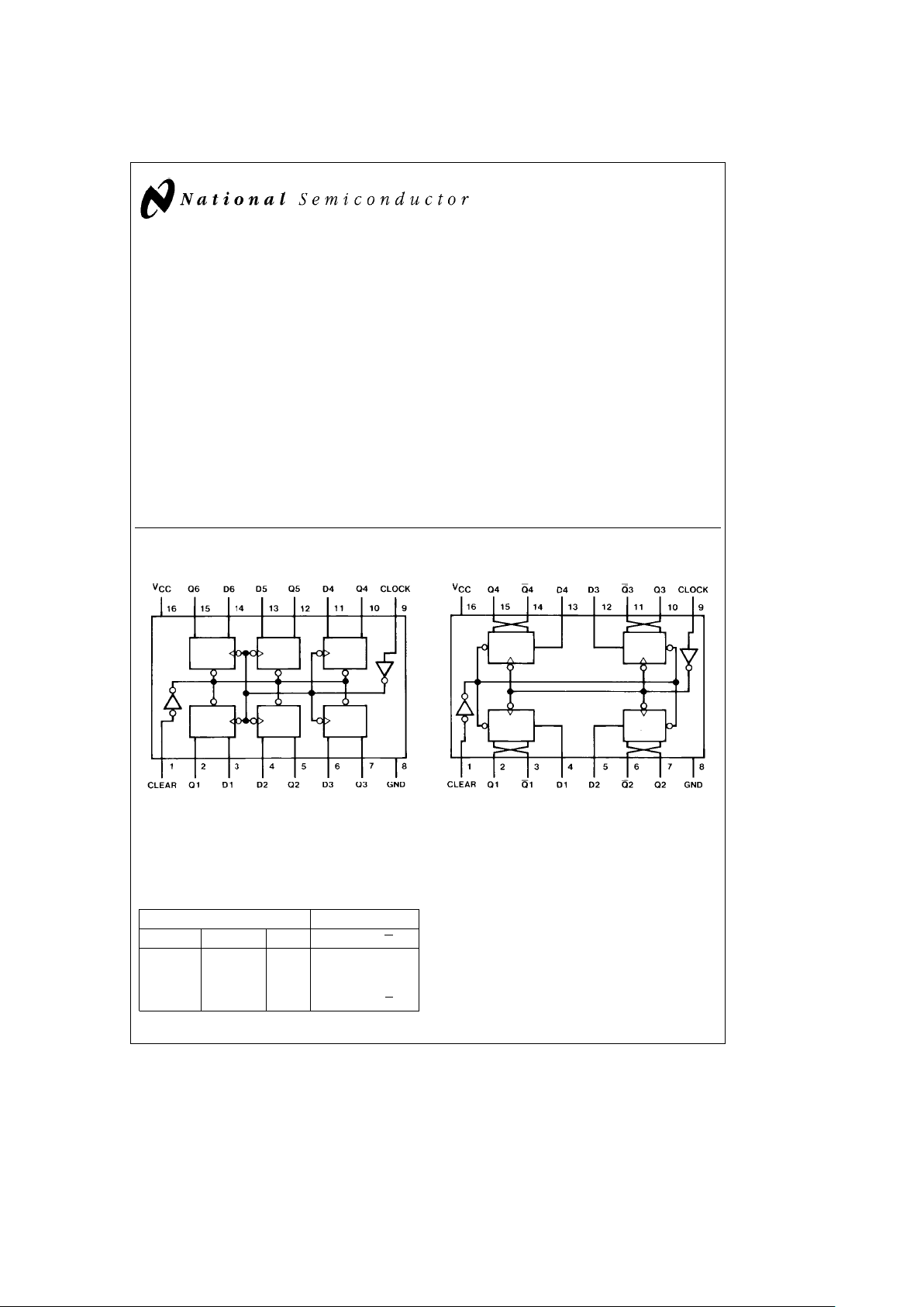
Connection Diagrams
Dual-In-Line Package
TL/F/6404– 1
Order Number 54LS174DMQB, 54LS174FMQB,
54LS174LMQB, DM54LS174J,
DM54LS174W, DM74LS174M or DM74LS174N
See NS Package Number E20A, J16A,
M16A, N16E or W16A
Dual-In-Line Package
TL/F/6404– 2
Order Number 54LS175DMQB, 54LS175FMQB,
54LS175LMQB, DM54LS175J
DM54LS175W, DM74LS175M or DM74LS175N
See NS Package Number E20A, J16A,
M16A, N16E or W16A
Function Table (Each Flip-Flop)
Inputs Outputs
Clear Clock D Q Q
²
LXXLH
H
u
HH L
H
u
LL H
HLXQ
0
Q
0
H
e
High Level (steady state)
L
e
Low Level (steady state)
X
e
Don’t Care
u
e
Transition from low to high level
Q
0
e
The level of Q before the indicated steady-state input conditions were
established.
²
e
LS175 only
C
1995 National Semiconductor Corporation RRD-B30M105/Printed in U. S. A.
Page 2
Absolute Maximum Ratings (Note)
If Military/Aerospace specified devices are required,
please contact the National Semiconductor Sales
Office/Distributors for availability and specifications.
Supply Voltage 7V
Input Voltage 7V
Operating Free Air Temperature Range
DM54LS and 54LS
b
55§Ctoa125§C
DM74LS 0
§
Ctoa70§C
Storage Temperature Range
b
65§Ctoa150§C
Note:
The ‘‘Absolute Maximum Ratings’’ are those values
beyond which the safety of the device cannot be guaranteed. The device should not be operated at these limits. The
parametric values defined in the ‘‘Electrical Characteristics’’
table are not guaranteed at the absolute maximum ratings.
The ‘‘Recommended Operating Conditions’’ table will define
the conditions for actual device operation.
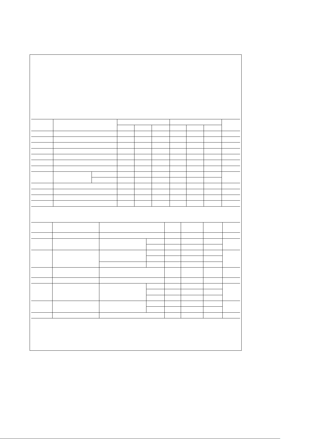
Recommended Operating Conditions
Symbol Parameter
DM54LS174 DM74LS174
Units
Min Nom Max Min Nom Max
V
CC
Supply Voltage 4.5 5 5.5 4.75 5 5.25 V
V
IH
High Level Input Voltage 2 2 V
V
IL
Low Level Input Voltage 0.7 0.8 V
I
OH
High Level Output Current
b
0.4
b
0.4 mA
I
OL
Low Level Output Current 4 8 mA
f
CLK
Clock Frequency (Note 1) 0 30 0 30 MHz
f
CLK
Clock Frequency (Note 2) 0 25 0 25 MHz
t
W
Pulse Width Clock 20 20
ns
(Note 6)
Clear 20 20
t
SU
Data Setup Time (Note 6) 20 20 ns
t
H
Data Hold Time (Note 6) 0 0 ns
t
REL
Clear Release Time (Note 6) 25 25 ns
T
A
Free Air Operating Temperature
b
55 125 0 70
§
C
’LS174 Electrical Characteristics
over recommended operating free air temperature range (unless otherwise noted)
Symbol Parameter Conditions Min
Typ
Max Units
(Note 3)
V
I
Input Clamp Voltage V
CC
e
Min, I
I
eb
18 mA
b
1.5 V
V
OH
High Level Output V
CC
e
Min, I
OH
e
Max DM54 2.5 3.4
V
Voltage V
IL
e
Max, V
IH
e
Min
DM74 2.7 3.4
V
OL
Low Level Output V
CC
e
Min, I
OL
e
Max DM54 0.25 0.4
Voltage V
IL
e
Max, V
IH
e
Min
DM74 0.35 0.5 V
I
OL
e
4 mA, V
CC
e
Min DM74 0.25 0.4
I
I
Input Current@Max V
CC
e
Max, V
I
e
7V
0.1 mA
Input Voltage
I
IH
High Level Input Current V
CC
e
Max, V
I
e
2.7V 20 mA
I
IL
Low Level Input V
CC
e
Max Clock
b
0.4
Current V
I
e
0.4V
Clear
b
0.4 mA
Data
b
0.36
I
OS
Short Circuit V
CC
e
Max DM54
b
20
b
100
mA
Output Current (Note 4)
DM74
b
20
b
100
I
CC
Supply Current V
CC
e
Max (Note 5) 16 26 mA
Note 1: C
L
e
15 pF, R
L
e
2kX,T
A
e
25§C and V
CC
e
5V.
Note 2: C
L
e
50 pF, R
L
e
2kX,T
A
e
25§C and V
CC
e
5V.
Note 3: All typicals are at V
CC
e
5V, T
A
e
25§C.
Note 4: Not more than one output should be shorted at a time, and the duration should not exceed one second.
Note 5: With all outputs open and 4.5V applied to all data and clear inputs, I
CC
is measured after a momentary ground, then 4.5V applied to the clock.
Note 6: T
A
e
25§C and V
CC
e
5V.
2
Page 3
’LS174 Switching Characteristics
at V
CC
e
5V and T
A
e
25§C (See Section 1 for Test Waveforms and Output Load)
From (Input)
R
L
e
2kX
Symbol Parameter
To (Output)
C
L
e
15 pF C
L
e
50 pF Units
Min Max Min Max
f
MAX
Maximum Clock Frequency 30 25 MHz
t
PLH
Propagation Delay Time Clock to
30 32 ns
Low to High Level Output Output
t
PHL
Propagation Delay Time Clock to
30 36 ns
High to Low Level Output Output
t
PHL
Propagation Delay Time Clear to
35 42 ns
High to Low Level Output Output
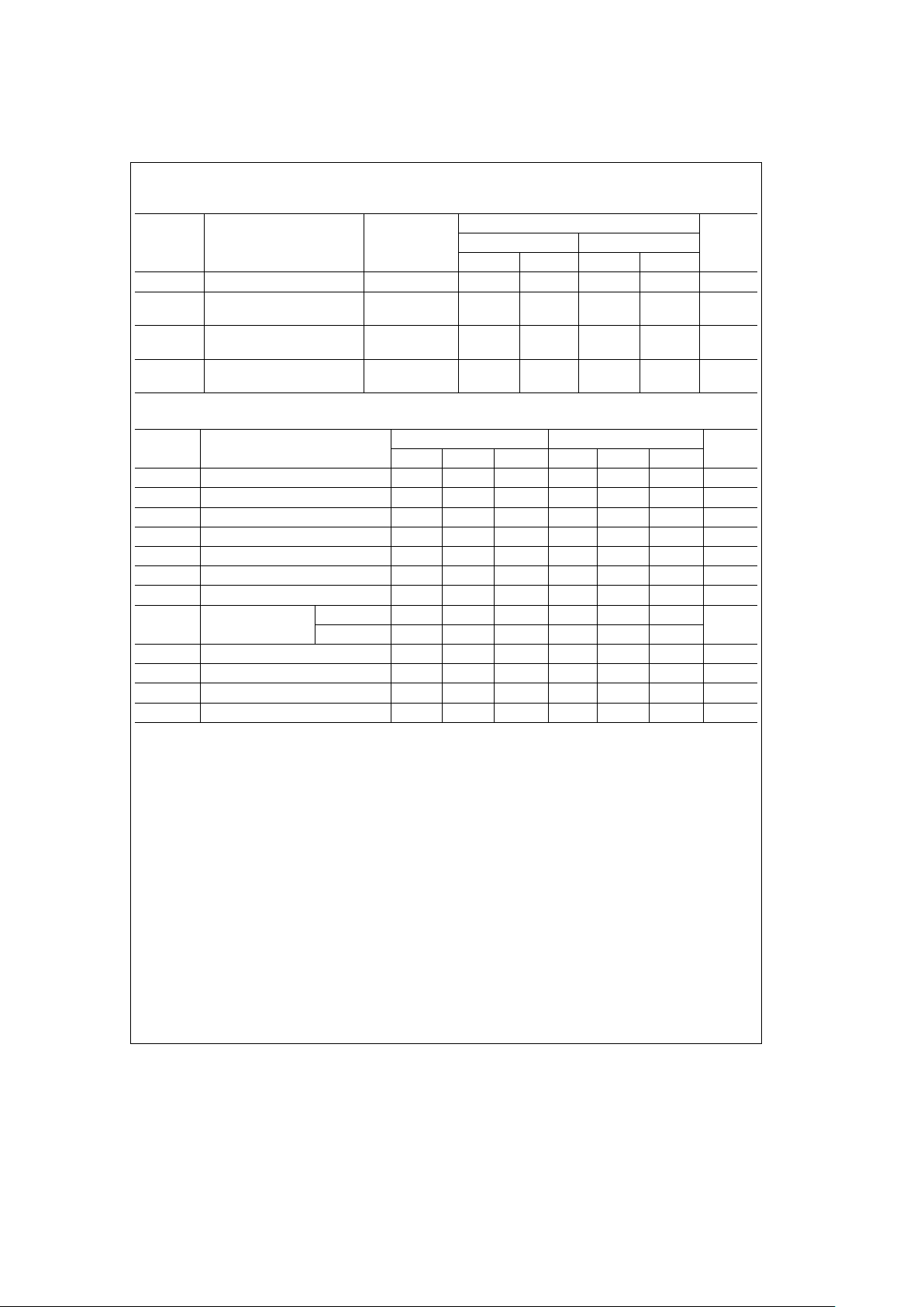
Recommended Operating Conditions
Symbol Parameter
DM54LS175 DM74LS175
Units
Min Nom Max Min Nom Max
V
CC
Supply Voltage 4.5 5 5.5 4.75 5 5.25 V
V
IH
High Level Input Voltage 2 2 V
V
IL
Low Level Input Voltage 0.7 0.8 V
I
OH
High Level Output Current
b
0.4
b
0.4 mA
I
OL
Low Level Output Current 4 8 mA
f
CLK
Clock Frequency (Note 1) 0 30 0 30 MHz
f
CLK
Clock Frequency (Note 2) 0 25 0 25 MHz
t
W
Pulse Width Clock 20 20
ns
(Note 3)
Clear 20 20
t
SU
Data Setup Time (Note 3) 20 20 ns
t
H
Data Hold Time (Note 3) 0 0 ns
t
REL
Clear Release Time (Note 3) 25 25 ns
T
A
Free Air Operating Temperature
b
55 125 0 70
§
C
Note 1: C
L
e
15 pF, R
L
e
2kX,T
A
e
25§C and V
CC
e
5V.
Note 2: C
L
e
50 pF, R
L
e
2kX,T
A
e
25§C and V
CC
e
5V.
Note 3: T
A
e
25§C and V
CC
e
5V.
3
Page 4

’LS175 Electrical Characteristics
over recommended operating free air temperature range (unless otherwise noted)
Symbol Parameter Conditions Min
Typ
Max Units
(Note 1)
V
I
Input Clamp Voltage V
CC
e
Min, I
I
eb
18 mA
b
1.5 V
V
OH
High Level Output V
CC
e
Min, I
OH
e
Max DM54 2.5 3.4
V
Voltage V
IL
e
Max, V
IH
e
Min
DM74 2.7 3.4
V
OL
Low Level Output V
CC
e
Min, I
OL
e
Max DM54 0.25 0.4
Voltage V
IL
e
Max, V
IH
e
Min
DM74 0.35 0.5 V
I
OL
e
4 mA, V
CC
e
Min DM74 0.25 0.4
I
I
Input Current@Max V
CC
e
Max, V
I
e
7V
0.1 mA
Input Voltage
I
IH
High Level Input Current V
CC
e
Max, V
I
e
2.7V 20 mA
I
IL
Low Level Input V
CC
e
Max Clock
b
0.4
Current V
I
e
0.4V
Clear
b
0.4 mA
Data
b
0.36
I
OS
Short Circuit V
CC
e
Max DM54
b
20
b
100
mA
Output Current (Note 2)
DM74
b
20
b
100
I
CC
Supply Current V
CC
e
Max (Note 3) 11 18 mA
’LS175 Switching Characteristics
at V
CC
e
5V and T
A
e
25§C (See Section 1 for Test Waveforms and Output Load)
From (Input)
R
L
e
2kX
Symbol Parameter
To (Output)
C
L
e
15 pF C
L
e
50 pF Units
Min Max Min Max
f
MAX
Maximum Clock Frequency 30 25 MHz
t
PLH
Propagation Delay Time Clock to
30 32 ns
Low to High Level Output Q or Q
t
PHL
Propagation Delay Time Clock to
30 36 ns
High to Low Level Output Q or Q
t
PLH
Propagation Delay Time Clear to
25 29 ns
Low to High Level Output Q
t
PHL
Propagation Delay Time Clear to
35 42 ns
High to Low Level Output Q
Note 1: All typicals are at V
CC
e
5V, T
A
e
25§C.
Note 2: Not more than one output should be shorted at a time, and the duration should not exceed one second.
Note 3: With all outputs open and 4.5V applied to all data and clear inputs, I
CC
is measured after a momentary ground, then 4.5V applied to the clock input.
4
Page 5

Logic Diagrams
LS174
TL/F/6404– 3
LS175
TL/F/6404– 4
5
Page 6

Physical Dimensions inches (millimeters)
Ceramic Leadless Chip Carrier (E)
Order Number 54LS174LMQB or 54LS175LMQB
NS Package Number E20A
16-Lead Ceramic Dual-In-Line Package (J)
Order Number DM54LS174DMQB, 54LS175DMQB, DM54LS174J or DM54LS175J
NS Package Number J16A
6
Page 7

Physical Dimensions inches (millimeters) (Continued)
16-Lead Small Outline Molded Package (M)
Order Number DM74LS174M or DM74LS175M
NS Package Number M16A
16-Lead Molded Dual-In-Line Package (N)
Order Number DM74LS174N or DM74LS175N
NS Package Number N16E
7
Page 8

54LS174/DM54LS174/DM74LS174, 54LS175/DM54LS175/DM74LS175
Hex/Quad D Flip-Flops with Clear
Physical Dimensions inches (millimeters) (Continued)
16-Lead Ceramic Flat Package (W)
Order Number 54LS174FMQB, 54LS175FMQB, DM54LS174W or DM54LS175W
NS Package Number W16A
LIFE SUPPORT POLICY
NATIONAL’S PRODUCTS ARE NOT AUTHORIZED FOR USE AS CRITICAL COMPONENTS IN LIFE SUPPORT
DEVICES OR SYSTEMS WITHOUT THE EXPRESS WRITTEN APPROVAL OF THE PRESIDENT OF NATIONAL
SEMICONDUCTOR CORPORATION. As used herein:
1. Life support devices or systems are devices or 2. A critical component is any component of a life
systems which, (a) are intended for surgical implant support device or system whose failure to perform can
into the body, or (b) support or sustain life, and whose be reasonably expected to cause the failure of the life
failure to perform, when properly used in accordance support device or system, or to affect its safety or
with instructions for use provided in the labeling, can effectiveness.
be reasonably expected to result in a significant injury
to the user.
National Semiconductor National Semiconductor National Semiconductor National Semiconductor
Corporation Europe Hong Kong Ltd. Japan Ltd.
1111 West Bardin Road Fax: (
a
49) 0-180-530 85 86 13th Floor, Straight Block, Tel: 81-043-299-2309
Arlington, TX 76017 Email: cnjwge@tevm2.nsc.com Ocean Centre, 5 Canton Rd. Fax: 81-043-299-2408
Tel: 1(800) 272-9959 Deutsch Tel: (
a
49) 0-180-530 85 85 Tsimshatsui, Kowloon
Fax: 1(800) 737-7018 English Tel: (
a
49) 0-180-532 78 32 Hong Kong
Fran3ais Tel: (
a
49) 0-180-532 93 58 Tel: (852) 2737-1600
Italiano Tel: (
a
49) 0-180-534 16 80 Fax: (852) 2736-9960
National does not assume any responsibility for use of any circuitry described, no circuit patent licenses are implied and National reserves the right at any time without notice to change said circuitry and specifications.
 Loading...