

Page 1
TL/F/6399
DM54LS165/DM74LS165 8-Bit Parallel In/Serial Output Shift Registers
May 1992
DM54LS165/DM74LS165 8-Bit Parallel
In/Serial Output Shift Registers
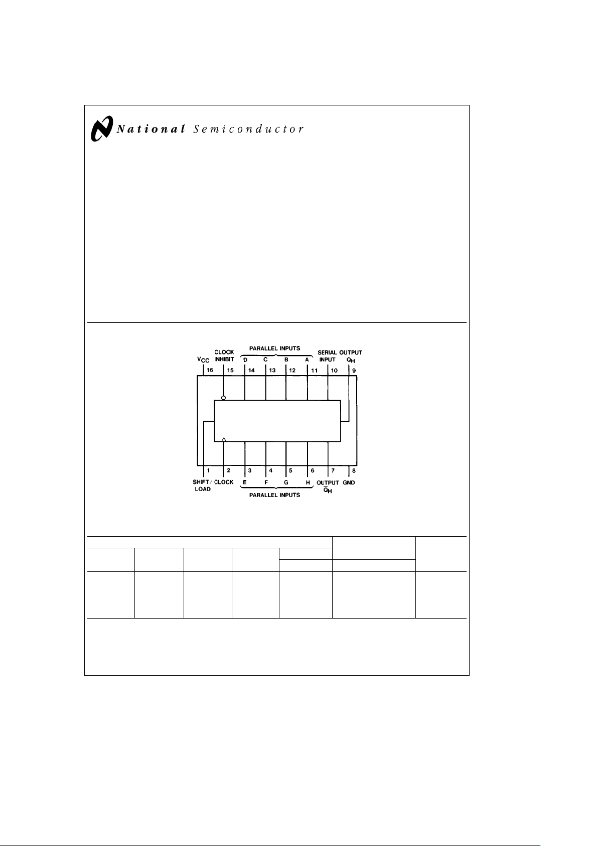
General Description
This device is an 8-bit serial shift register which shifts data in
the direction of Q
A
toward QHwhen clocked. Parallel-in access is made available by eight individual direct data inputs,
which are enabled by a low level at the shift/load input.
These registers also feature gated clock inputs and complementary outputs from the eighth bit.
Clocking is accomplished through a 2-input NOR gate, permitting one input to be used as a clock-inhibit function. Holding either of the clock inputs high inhibits clocking, and holding either clock input low with the load input high enables
the other clock input. The clock-inhibit input should be
changed to the high level only while the clock input is high.
Parallel loading is inhibited as long as the load input is high.
Data at the parallel inputs are loaded directly into the register on a high-to-low transition of the shift/load input, regardless of the logic levels on the clock, clock inhibit, or serial
inputs.
Features
Y
Complementary outputs
Y
Direct overriding (data) inputs
Y
Gated clock inputs
Y
Parallel-to-serial data conversion
Y
Typical frequency 35 MHz
Y
Typical power dissipation 105 mW
Connection Diagram
Dual-In-Line Package
TL/F/6399– 1
Order Number DM54LS165J, DM54LS165W, DM74LS165WM or DM74LS165N
See NS Package Number J16A, M16B, N16E or W16A
Function Table
Inputs Internal
Shift/ Clock
Clock Serial
Parallel
Outputs Output
Load Inhibit
A...H Q
A
Q
B
Q
H
L X X X a...h a b h
HLLX XQ
A0
Q
B0
Q
H0
HL
u
HXHQAnQ
Gn
HL
u
LXLQAnQ
Gn
HHXX XQA0Q
B0
Q
H0
HeHigh Level (steady state), LeLow Level (steady state)
X
e
Don’t Care (any input, including transitions)
u
e
Transition from low-to-high level
a...h
e
The level of steady-state input at inputs A through H, respectively.
Q
A0,QB0,QH0
e
The level of QA,QB,orQH, respectively, before the indicated steady-state input conditions were established.
Q
An,QGn
e
The level of QAor QG, respectively, before the most recentutransition of the clock.
C
1995 National Semiconductor Corporation RRD-B30M105/Printed in U. S. A.
Page 2
Absolute Maximum Ratings (Note)
If Military/Aerospace specified devices are required,
please contact the National Semiconductor Sales
Office/Distributors for availability and specifications.
Supply Voltage 7V
Input Voltage 7V
Operating Free Air Temperature Range
DM54LS
b
55§Ctoa125§C
DM74LS 0
§
Ctoa70§C
Storage Temperature Range
b
65§Ctoa150§C
Note:
The ‘‘Absolute Maximum Ratings’’ are those values
beyond which the safety of the device cannot be guaranteed. The device should not be operated at these limits. The
parametric values defined in the ‘‘Electrical Characteristics’’
table are not guaranteed at the absolute maximum ratings.
The ‘‘Recommended Operating Conditions’’ table will define
the conditions for actual device operation.
Recommended Operating Conditions
Symbol Parameter
DM54LS165 DM74LS165
Units
Min Nom Max Min Nom Max
V
CC
Supply Voltage 4.5 5 5.5 4.75 5 5.25 V
V
IH
High Level Input Voltage 2 2 V
V
IL
Low Level Input Voltage 0.7 0.8 V
I
OH
High Level Output Current
b
0.4
b
0.4 mA
I
OL
Low Level Output Current 4 8 mA
f
CLK
Clock Frequency (Note 1) 30 0 25 MHz
f
CLK
Clock Frequency (Note 2) 0 20 MHz
t
W
Pulse Width Clock 18 25
ns
(Note 2)
Load 15 15
t
SU
Setup Time Parallel 10 10
(Note 6)
Serial 10 20
ns
Enable 10 30
Shift 10 45
t
H
Hold Time (Note 6) 5 0 ns
T
A
Free Air Operating Temperature
b
55 125 0 70
§
C
Electrical Characteristics over recommended operating free air temperature range (unless otherwise noted)
Symbol Parameter Conditions Min
Typ
Max Units
(Note 3)
V
I
Input Clamp Voltage V
CC
e
Min, I
I
eb
18 mA
b
1.5 V
V
OH
High Level Output V
CC
e
Min, I
OH
e
Max DM54 2.5
V
Voltage V
IL
e
Max, V
IH
e
Min
DM74 2.7 3.4
V
OL
Low Level Output V
CC
e
Min, I
OL
e
Max DM54 0.4
Voltage V
IL
e
Max, V
IH
e
Min
DM74 0.35 0.5 V
I
OL
e
4 mA, V
CC
e
Min 0.25 0.4
I
I
Input Current@Max V
CC
e
Max, V
I
e
7V (DM74) Shift/Load 0.3
mA
Input Voltage V
I
e
10V (DM54)
Others 0.1
I
IH
High Level Input V
CC
e
Max Shift/Load 60
mA
Current V
I
e
2.7V
Others 20
I
IL
Low Level Input V
CC
e
Max Shift/Load
b
1.2
mA
Current V
I
e
0.4V
Others
b
0.4
I
OS
Short Circuit V
CC
e
Max DM54
b
20
b
100
mA
Output Current (Note 4)
DM74
b
20
b
100
I
CC
Supply Current V
CC
e
Max (Note 5) 21 36 mA
Note 1: C
L
e
15 pF, R
L
e
2kX,T
A
e
25§C and V
CC
e
5V
Note 2: C
L
e
50 pF, R
L
e
2kX,T
A
e
25§C and V
CC
e
5V
Note 3: All typicals are at V
CC
e
5V, T
A
e
25§C.
Note 4: Not more than one output should be shorted at a time, and the duration should not exceed one second.
Note 5: With all outputs open, clock inhibit and shift/load at 4.5V, and a clock pulse applied to the CLOCK input, I
CC
is measured first with the parallel inputs at
4.5V, then again grounded.
Note 6: T
A
e
25§C and V
CC
e
5V.
2
Page 3

Switching Characteristics at V
CC
e
5V and T
A
e
25§C
DM54LS DM74LS DM74LS
Symbol Parameter
From (Input)
C
L
e
15 pF C
L
e
15 pF
R
L
e
2kX
Units
To (Output) C
L
e
50 pF
Min Max Min Max Min Max
f
MAX
Maximum Clock Frequency 25 25 20 MHz
t
PLH
Propagation Delay Time Load to
30 35 37 ns
Low to High Level Output Any Q
t
PHL
Propagation Delay Time Load to
30 35 42 ns
High to Low Level Output Any Q
t
PLH
Propagation Delay Time Clock to
30 40 42 ns
Low to High Level Output Any Q
t
PHL
Propagation Delay Time Clock to
30 40 47 ns
High to Low Level Output Any Q
t
PLH
Propagation Delay Time H
20 25 27 ns
Low to High Level Output to Q
H
t
PHL
Propagation Delay Time H
30 30 37 ns
High to Low Level Output to Q
H
t
PLH
Propagation Delay Time H
30 30 32 ns
Low to High Level Output to Q
H
t
PHL
Propagation Delay Time H
25 25 32 ns
High to Low Level Output to Q
H
Timing Diagram
Typical Shift, Load, and Inhibit Sequences
TL/F/6399– 3
3
Page 4

Logic Diagram
TL/F/6399– 2
4
Page 5

Physical Dimensions inches (millimeters)
16-Lead Ceramic Dual-In-Line Package (J)
Order Number DM54LS165J
NS Package Number J16A
16-Lead Wide Small Outline Molded Package (M)
Order Number DM74LS165WM
NS Package Number M16B
5
Page 6

DM54LS165/DM74LS165 8-Bit Parallel In/Serial Output Shift Registers
Physical Dimensions inches (millimeters) (Continued)
16-Lead Molded Dual-In-Line Package (N)
Order Number DM74LS165N
NS Package Number N16E
16-Lead Ceramic Flat Package (W)
Order Number DM54LS165W
NS Package Number W16A
LIFE SUPPORT POLICY
NATIONAL’S PRODUCTS ARE NOT AUTHORIZED FOR USE AS CRITICAL COMPONENTS IN LIFE SUPPORT
DEVICES OR SYSTEMS WITHOUT THE EXPRESS WRITTEN APPROVAL OF THE PRESIDENT OF NATIONAL
SEMICONDUCTOR CORPORATION. As used herein:
1. Life support devices or systems are devices or 2. A critical component is any component of a life
systems which, (a) are intended for surgical implant support device or system whose failure to perform can
into the body, or (b) support or sustain life, and whose be reasonably expected to cause the failure of the life
failure to perform, when properly used in accordance support device or system, or to affect its safety or
with instructions for use provided in the labeling, can effectiveness.
be reasonably expected to result in a significant injury
to the user.
National Semiconductor National Semiconductor National Semiconductor National Semiconductor
Corporation Europe Hong Kong Ltd. Japan Ltd.
1111 West Bardin Road Fax: (
a
49) 0-180-530 85 86 13th Floor, Straight Block, Tel: 81-043-299-2309
Arlington, TX 76017 Email: cnjwge@tevm2.nsc.com Ocean Centre, 5 Canton Rd. Fax: 81-043-299-2408
Tel: 1(800) 272-9959 Deutsch Tel: (
a
49) 0-180-530 85 85 Tsimshatsui, Kowloon
Fax: 1(800) 737-7018 English Tel: (
a
49) 0-180-532 78 32 Hong Kong
Fran3ais Tel: (
a
49) 0-180-532 93 58 Tel: (852) 2737-1600
Italiano Tel: (
a
49) 0-180-534 16 80 Fax: (852) 2736-9960
National does not assume any responsibility for use of any circuitry described, no circuit patent licenses are implied and National reserves the right at any time without notice to change said circuitry and specifications.
 Loading...