

Page 1
TL/F/6397
54LS161A/DM54LS161A/DM74LS161A, 54LS163A/DM54LS163A/DM74LS163A Synchronous
4-Bit Binary Counters
May 1992
54LS161A/DM54LS161A/DM74LS161A,
54LS163A/DM54LS163A/DM74LS163A
Synchronous 4-Bit Binary Counters
General Description
These synchronous, presettable counters feature an internal carry look-ahead for application in high-speed counting
designs. The LS161A and LS163A are 4-bit binary counters.
The carry output is decoded by means of a NOR gate, thus
preventing spikes during the normal counting mode of operation. Synchronous operation is provided by having all flipflops clocked simultaneously so that the outputs change coincident with each other when so instructed by the countenable inputs and internal gating. This mode of operation
eliminates the output counting spikes which are normally
associated with asynchronous (ripple clock) counters. A
buffered clock input triggers the four flip-flops on the rising
(positive-going) edge of the clock input waveform.
These counters are fully programmable; that is, the outputs
may be preset to either level. As presetting is synchronous,
setting up a low level at the load input disables the counter
and causes the outputs to agree with the setup data after
the next clock pulse, regardless of the levels of the enable
input. The clear function for the LS161A is asynchronous;
and a low level at the clear input sets all four of the flip-flop
outputs low, regardless of the levels of clock, load, or enable inputs. The clear function for the LS163A is synchronous; and a low level at the clear inputs sets all four of the
flip-flop outputs low after the next clock pulse, regardless of
the levels of the enable inputs. This synchronous clear allows the count length to be modified easily, as decoding the
maximum count desired can be accomplished with one external NAND gate. The gate output is connected to the clear
input to synchronously clear the counter to all low outputs.
The carry look-ahead circuitry provides for cascading counters for n-bit synchronous applications without additional
gating. Instrumental in accomplishing this function are two
count-enable inputs and a ripple carry output.
Both count-enable inputs (P and T) must be high to count,
and input T is fed forward to enable the ripple carry output.
The ripple carry output thus enabled will produce a high-level output pulse with a duration approximately equal to the
high-level portion of the Q
A
output. This high-level overflow
ripple carry pulse can be used to enable successive cascaded stages. High-to-low level transitions at the enable P or T
inputs may occur, regardless of the logic level of the clock.
These counters feature a fully independent clock circuit.
Changes made to control inputs (enable P or T or load) that
will modify the operating mode have no effect until clocking
occurs. The function of the counter (whether enabled, disabled, loading, or counting) will be dictated solely by the
conditions meeting the stable set-up and hold times.
Features
Y
Synchronously programmable
Y
Internal look-ahead for fast counting
Y
Carry output for n-bit cascading
Y
Synchronous counting
Y
Load control line
Y
Diode-clamped inputs
Y
Typical propagation time, clock to Q output 14 ns
Y
Typical clock frequency 32 MHz
Y
Typical power dissipation 93 mW
Y
Alternate Military/Aerospace device (54LS161,
54LS163) is available. Contact a National Semiconductor Sales Office/Distributor for specificaitons.
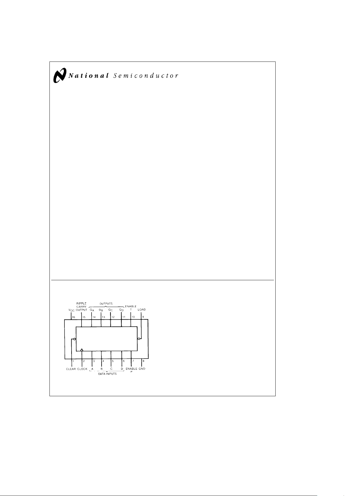
Connection Diagram
Dual-In-Line Package
TL/F/6397– 1
Order Numbers 54LS161ADMQB, 54LS161AFMQB,
54LS161ALMQB, 54LS163ADMQB, 54LS163AFMQB,
54LS163ALMQB, DM54LS161AJ, DM54LS161AW,
DM54LS163AJ, DM54LS163AW, DM74LS161AM,
DM74LS161AN, DM74LS163AM or DM74LS163AN
See NS Package Number E20A, J16A,
M16A, N16E or W16A
C
1995 National Semiconductor Corporation RRD-B30M105/Printed in U. S. A.
Page 2
Absolute Maximum Ratings (Note)
If Military/Aerospace specified devices are required,
please contact the National Semiconductor Sales
Office/Distributors for availability and specifications.
Supply Voltage 7V
Input Voltage 7V
Operating Free Air Temperature Range
DM54LS and 54LS
b
55§Ctoa125§C
DM74LS 0
§
Ctoa70§C
Storage Temperature Range
b
65§Ctoa150§C
Note:
The ‘‘Absolute Maximum Ratings’’ are those values
beyond which the safety of the device cannot be guaranteed. The device should not be operated at these limits. The
parametric values defined in the ‘‘Electrical Characteristics’’
table are not guaranteed at the absolute maximum ratings.
The ‘‘Recommended Operating Conditions’’ table will define
the conditions for actual device operation.
Recommended Operating Conditions
Symbol Parameter
DM54LS161A DM74LS161A
Units
Min Nom Max Min Nom Max
V
CC
Supply Voltage 4.5 5 5.5 4.75 5 5.25 V
V
IH
High Level Input Voltage 2 2 V
V
IL
Low Level Input Voltage 0.7 0.8 V
I
OH
High Level Output Current
b
0.4
b
0.4 mA
I
OL
Low Level Output Current 4 8 mA
f
CLK
Clock Frequency (Note 1) 0 25 0 25 MHz
Clock Frequency (Note 2) 0 20 0 20 MHz
t
W
Pulse Width Clock 20 6 20 6
ns
(Note 1)
Clear 20 9 20 9
Pulse Width Clock 25 25
ns
(Note 2)
Clear 25 25
t
SU
Setup Time Data 20 8 20 8
(Note 1)
Enable P 25 17 25 17 ns
Load 25 15 25 15
Setup Time Data 20 20
(Note 2)
Enable P 30 30 ns
Load 30 30
t
H
Hold Time Data 0
b
30
b
3
ns
(Note 1)
Others 0
b
30
b
3
Hold Time Data 5 5
ns
(Note 2)
Others 5 5
t
REL
Clear Release Time (Note 1) 20 20 ns
Clear Release Time (Note 2) 25 25 ns
T
A
Free Air Operating Temperature
b
55 125 0 70
§
C
Note 1: C
L
e
15 pF, R
L
e
2kX,T
A
e
25§C and V
CC
e
5.5V.
Note 2: C
L
e
50 pF, R
L
e
2kX,T
A
e
25§C and V
CC
e
5.5V.
2
Page 3
’LS161 Electrical Characteristics
over recommended operating free air temperature range (unless otherwise noted)
Symbol Parameter Conditions Min
Typ
Max Units
(Note 1)
V
I
Input Clamp Voltage V
CC
e
Min, I
I
eb
18 mA
b
1.5 V
V
OH
High Level Output V
CC
e
Min, I
OH
e
Max DM54 2.5 3.4
V
Voltage V
IL
e
Max, V
IH
e
Min
DM74 2.7 3.4
V
OL
Low Level Output V
CC
e
Min, I
OL
e
Max DM54 0.25 0.4
Voltage V
IL
e
Max, V
IH
e
Min
DM74 0.35 0.5 V
I
OL
e
4 mA, V
CC
e
Min DM74 0.25 0.4
I
I
Input Current@Max V
CC
e
Max Enable T 0.2
Input Voltage V
I
e
7V
Clock 0.2
mA
Load 0.2
Others 0.1
I
IH
High Level Input V
CC
e
Max Enable T 40
Current V
I
e
2.7V
Clock 40
mA
Load 40
Others 20
I
IL
Low Level Input V
CC
e
Max Enable T
b
0.8
Current V
I
e
0.4V
Clock
b
0.8
mA
Load
b
0.8
Others
b
0.4
I
OS
Short Circuit V
CC
e
Max DM54
b
20
b
100
mA
Output Current (Note 2)
DM74
b
20
b
100
I
CCH
Supply Current with V
CC
e
Max 18 31
mA
Outputs High (Note 3)
I
CCL
Supply Current with V
CC
e
Max
19 32 mA
Outputs Low (Note 4)
Note 1: All typicals are at V
CC
e
5V, T
A
e
25§C.
Note 2: Not more than one output should be shorted at a time, and the duration should not exceed one second.
Note 3: I
CCH
is measured with the load high, then again with the load low, with all other inputs high and all outputs open.
Note 4: I
CCL
is measured with the clock input high, then again with the clock input low, with all other inputs low and all outputs open.
’LS161 Switching Characteristics
at V
CC
e
5V and T
A
e
25§C (See Section 1 for Test Waveforms and Output Load)
From (Input)
R
L
e
2kX
Symbol Parameter
To (Output)
C
L
e
15 pF C
L
e
50 pF Units
Min Max Min Max
f
MAX
Maximum Clock Frequency 25 20 MHz
t
PLH
Propagation Delay Time Clock to
25 30 ns
Low to High Level Output Ripple Carry
t
PHL
Propagation Delay Time Clock to
30 38 ns
High to Low Level Output Ripple Carry
t
PLH
Propagation Delay Time Clock to Any Q
22 27 ns
Low to High Level Output (Load High)
t
PHL
Propagation Delay Time Clock to Any Q
27 38 ns
High to Low Level Output (Load High)
3
Page 4
’LS161 Switching Characteristics
at V
CC
e
5V and T
A
e
25§C (See Section 1 for Test Waveforms and Output Load) (Continued)
From (Input)
R
L
e
2kX
Symbol Parameter
To (Output)
C
L
e
15 pF C
L
e
50 pF Units
Min Max Min Max
t
PLH
Propagation Delay Time Clock to Any Q
24 30 ns
Low to High Level Output (Load Low)
t
PHL
Propagation Delay Time Clock to Any Q
27 38 ns
High to Low Level Output (Load Low)
t
PLH
Propagation Delay Time Enable T to
14 27 ns
Low to High Level Output Ripple Carry
t
PHL
Propagation Delay Time Enable T to
15 27 ns
High to Low Level Output Ripple Carry
t
PHL
Propagation Delay Time Clear to
28 45 ns
High to Low Level Output Any Q
Recommended Operating Conditions
Symbol Parameter
DM54LS163A DM74LS163A
Units
Min Nom Max Min Nom Max
V
CC
Supply Voltage 4.5 5 5.5 4.75 5 5.25 V
V
IH
High Level Input Voltage 2 2 V
V
IL
Low Level Input Voltage 0.7 0.8 V
I
OH
High Level Output Current
b
0.4
b
0.4 mA
I
OL
Low Level Output Current 4 8 mA
f
CLK
Clock Frequency (Note 1) 0 25 0 25 MHz
Clock Frequency (Note 2) 0 20 0 20 MHz
t
W
Pulse Width Clock 20 6 20 6
ns
(Note 1)
Clear 20 9 20 9
Pulse Width Clock 25 25
ns
(Note 2)
Clear 25 25
t
SU
Setup Time Data 20 8 20 8
(Note 1)
Enable P 25 17 25 17 ns
Load 25 15 25 15
Setup Time Data 20 20
(Note 2)
Enable P 30 30 ns
Load 30 30
t
H
Hold Time Data 0
b
30
b
3
ns
(Note 1)
Others 0
b
30
b
3
Hold Time Data 5 5
ns
(Note 2)
Others 5 5
t
REL
Clear Release Time (Note 1) 20 20 ns
Clear Release Time (Note 2) 25 25 ns
T
A
Free Air Operating Temperature
b
55 125 0 70
§
C
Note 1: C
L
e
15 pF, R
L
e
2kX,T
A
e
25§C and V
CC
e
5V.
Note 2: C
L
e
50 pF, R
L
e
2kX,T
A
e
25§C and V
CC
e
5V.
4
Page 5

’LS163 Electrical Characteristics
over recommended operating free air temperature range (unless otherwise noted)
Symbol Parameter Conditions Min
Typ
Max Units
(Note 1)
V
I
Input Clamp Voltage V
CC
e
Min, I
I
eb
18 mA
b
1.5 V
V
OH
High Level Output V
CC
e
Min, I
OH
e
Max DM54 2.5 3.4
V
Voltage V
IL
e
Max, V
IH
e
Min
DM74 2.7 3.4
V
OL
Low Level Output V
CC
e
Min, I
OL
e
Max DM54 0.25 0.4
Voltage V
IL
e
Max, V
IH
e
Min
DM74 0.35 0.5 V
I
OL
e
4 mA, V
CC
e
Min DM74 0.25 0.4
I
I
Input Current@Max V
CC
e
Max Enable T 0.2
Input Voltage V
I
e
7V
Clock, Clear 0.2
mA
Load 0.2
Others 0.1
I
IH
High Level Input V
CC
e
Max Enable T 40
Current V
I
e
2.7V
Load 40
mA
Clock, Clear 40
Others 20
I
IL
Low Level Input V
CC
e
Max Enable T
b
0.8
Current V
I
e
0.4V
Clock, Clear
b
0.8
mA
Load
b
0.8
Others
b
0.4
I
OS
Short Circuit V
CC
e
Max DM54
b
20
b
100
mA
Output Current (Note 2)
DM74
b
20
b
100
I
CCH
Supply Current with V
CC
e
Max 18 31
mA
Outputs High (Note 3)
I
CCL
Supply Current with V
CC
e
Max
18 32 mA
Outputs Low (Note 4)
Note 1: All typicals are at V
CC
e
5V, T
A
e
25§C.
Note 2: Not more than one output should be shorted at a time, and the duration should not exceed one second.
Note 3: I
CCH
is measured with the load high, then again with the load low, with all other inputs high and all outputs open.
Note 4: I
CCL
is measured with the clock input high, then again with the clock input low, with all other inputs low and all outputs open.
’LS163 Switching Characteristics
at V
CC
e
5V and T
A
e
25§C (See Section 1 for Test Waveforms and Output Load)
From (Input)
R
L
e
2kX
Symbol Parameter
To (Output)
C
L
e
15 pF C
L
e
50 pF Units
Min Max Min Max
f
MAX
Maximum Clock Frequency 25 20 MHz
t
PLH
Propagation Delay Time Clock to
25 30 ns
Low to High Level Output Ripple Carry
t
PHL
Propagation Delay Time Clock to
30 38 ns
High to Low Level Output Ripple Carry
t
PLH
Propagation Delay Time Clock to Any Q
22 27 ns
Low to High Level Output (Load High)
t
PHL
Propagation Delay Time Clock to Any Q
27 38 ns
High to Low Level Output (Load High)
5
Page 6

’LS163 Switching Characteristics
at V
CC
e
5V and T
A
e
25§C (See Section 1 for Test Waveforms and Output Load) (Continued)
From (Input)
R
L
e
2kX
Symbol Parameter
To (Output)
C
L
e
15 pF C
L
e
50 pF Units
Min Max Min Max
t
PLH
Propagation Delay Time Clock to Any Q
24 30 ns
Low to High Level Output (Load Low)
t
PHL
Propagation Delay Time Clock to Any Q
27 38 ns
High to Low Level Output (Load Low)
t
PLH
Propagation Delay Time Enable T to
14 27 ns
Low to High Level Output Ripple Carry
t
PHL
Propagation Delay Time Enable T to
15 27 ns
High to Low Level Output Ripple Carry
t
PHL
Propagation Delay Time Clear to Any Q
28 45 ns
High to Low Level Output (Note 1)
Note 1: The propagation delay clear to output is measured from the clock input transition.
Logic Diagram
LS163A
TL/F/6397– 2
The LS161A is similar, however, the clear buffer is connected directly to the flip flops.
6
Page 7

Parameter Measurement Information
Switching Time Waveforms
TL/F/6397– 3
Note A: The input pulses are supplied by generators having the following characteristics: PRRs1 MHz, duty cycles50%, Z
OUT
&
50X,t
r
s
10 ns, t
f
s
10 ns.
Vary PRR to measure f
MAX
.
Note B: Outputs Q
D
and carry are tested at t
na16
where tnis the bit time when all outputs are low.
Note C: V
REF
e
1.5V.
Switching Time Waveforms
TL/F/6397– 4
Note A: The input pulses are supplied by generators having the following characteristics: PRRs1 MHz, duty cycles50%, Z
OUT
&
50X,t
r
s
6 ns, t
f
s
6 ns. Vary
PRR to measure f
MAX
.
Note B: Enable P and enable T setup times are measured at t
na0
.
Note C: V
REF
e
1.3V.
7
Page 8

Timing Diagram
LS161A, LS163A Synchronous Binary Counters
Typical Clear, Preset, Count and Inhibit Sequences
TL/F/6397– 5
Sequence:
(1) Clear outputs to zero
(2) Preset to binary twelve
(3) Count to thirteen, fourteen, fifteen, zero, one, and two
(4) Inhibit
8
Page 9

9
Page 10

Physical Dimensions inches (millimeters)
Ceramic Leadless Chip Carrier Package (E)
Order Numbers 54LS161ALMQB or 54LS163ALMQB
NS Package Number E20A
16-Lead Ceramic Dual-In-Line Package (J)
Order Numbers 54LS161ADMQB, 54LS163ADMQB, DM54LS161AJ or DM54LS163AJ
NS Package Number J16A
10
Page 11

Physical Dimensions inches (millimeters) (Continued)
16-Lead Small Outline Molded Package (M)
Order Number DM74LS161AM or DM74LS163AM
NS Package Number M16A
16-Lead Molded Dual-In-Line Package (N)
Order Numbers DM74LS161AN, DM74LS163AN
NS Package Number N16E
11
Page 12

54LS161A/DM54LS161A/DM74LS161A, 54LS163A/DM54LS163A/DM74LS163A Synchronous
4-Bit Binary Counters
Physical Dimensions inches (millimeters) (Continued)
16-Lead Ceramic Flat Package (W)
Order Numbers 54LS161AFMQB, 54LS163AFMQB,
DM54LS161AN or DM54LS163AW
NS Package Number W16A
LIFE SUPPORT POLICY
NATIONAL’S PRODUCTS ARE NOT AUTHORIZED FOR USE AS CRITICAL COMPONENTS IN LIFE SUPPORT
DEVICES OR SYSTEMS WITHOUT THE EXPRESS WRITTEN APPROVAL OF THE PRESIDENT OF NATIONAL
SEMICONDUCTOR CORPORATION. As used herein:
1. Life support devices or systems are devices or 2. A critical component is any component of a life
systems which, (a) are intended for surgical implant support device or system whose failure to perform can
into the body, or (b) support or sustain life, and whose be reasonably expected to cause the failure of the life
failure to perform, when properly used in accordance support device or system, or to affect its safety or
with instructions for use provided in the labeling, can effectiveness.
be reasonably expected to result in a significant injury
to the user.
National Semiconductor National Semiconductor National Semiconductor National Semiconductor
Corporation Europe Hong Kong Ltd. Japan Ltd.
1111 West Bardin Road Fax: (
a
49) 0-180-530 85 86 13th Floor, Straight Block, Tel: 81-043-299-2309
Arlington, TX 76017 Email: cnjwge@tevm2.nsc.com Ocean Centre, 5 Canton Rd. Fax: 81-043-299-2408
Tel: 1(800) 272-9959 Deutsch Tel: (
a
49) 0-180-530 85 85 Tsimshatsui, Kowloon
Fax: 1(800) 737-7018 English Tel: (
a
49) 0-180-532 78 32 Hong Kong
Fran3ais Tel: (
a
49) 0-180-532 93 58 Tel: (852) 2737-1600
Italiano Tel: (
a
49) 0-180-534 16 80 Fax: (852) 2736-9960
National does not assume any responsibility for use of any circuitry described, no circuit patent licenses are implied and National reserves the right at any time without notice to change said circuitry and specifications.
 Loading...