

Page 1

CX74037
Transmit RF IC for TDMA or AMPS Applications
Conexant’s CX74037 Transmit RF Application-Specific Integrated Circuit (ASIC) is
a triple-mode, dual-band transmitter intended for use in IS-136 compliant cellular
phones. As a dual mode IC, it can be used in Time Division Multiple Access
(TDMA) mode or Advanced Mobile Phone System (AMPS) mode. The device is
available in a 48-pin 7x7 Land Grid Array (LGA) package with downset paddle.
The CX74037 RF IC device includes the following functional components:
•
In-Phase and Quadrature (I/Q) modulator
•
Two Intermediate Frequency (IF) Voltage Controlled Oscillator (VCO) inputs
•
IF Variable Gain Amplifier (VGA)
•
Two upconverters
•
Two drivers for external Power Amplifiers (PAs).
The CX74037 48-pin, 7x7 LGA package pin configuration is shown in Figure 1. A
CX74037 block diagram is shown in Figure 2.
VGA_EN
LO_CELL
VCC_MIX
MIX_IN+
MIX_INVCC_IF
VGA_GC
VGA_OUT-
VGA_OUT+
VCC_LD_PCS
POT_CELL
DRV_ENA
RF_PCS_OUT
VCC_BIAS
RF_CELL_OUT
BAND
1
2
3
4
5
6
7
8
9
10
11
12
13
LO_PCS_INNCNC
45464748 44 43 42 41 40 39 38
17161514 18 19 20 21 22 23 24
IF_SELECT
IF_VCO_IN2-
IF_VCO_IN2+
Features
• Sectional enable lines for independent control of
circuits within the chip
• 90 dB IF VGA range
• Separate IF frequencies can be used for the 800
MHz (AMPS) and 1900 MHz Bands (PCS)
• Dual drivers for 800 MHz and 1900 MHz
• PA driver is deactivated by using the Driver Enable
signal when there is no transmission
• Available in a 48-pin, 7x7 LGA package with
downset paddle
Applications
• Cellular and/or PCS-band phones
• TDMA and/or AMPS-mode phones
• Portable battery powered equipment
MODE
NC
37
36
35
34
33
32
31
30
29
28
27
26
25
NC
IF_VCO_IN1IF_VCO_IN1+
NC
NC
NC
VCC_DIV
MIX_CELL_OUT
PULL_ENA
VCC_DIFF_DRV
MIX_PCS_OUT
NC
NC
Data Sheet
NC
I_DATA-
POT_PCS
VCC_MID_PCS
VCC_DRV_CEL
I_DATA+
DRV_PCS_IN
DRV_CELL_IN
Q_DATA+
VCC_MOD
Q_DATA-
101103A-1_080400
Figure 1. CX74037 48-Pin, 7x7 LGA Package Pin Configuration
Conexant Proprietary
Data Subject to Change September 27, 2000
Doc. No. 101103A
Page 2
CX74037 Transmit RF IC for TDMA or AMPS Applications
PCS RF SAW
PCS LO
PCS-TDMA
RF Out
Cell RF Out
Cell RF SAW
Figure 2. CX74037 Functional Block Diagram
Cell LO
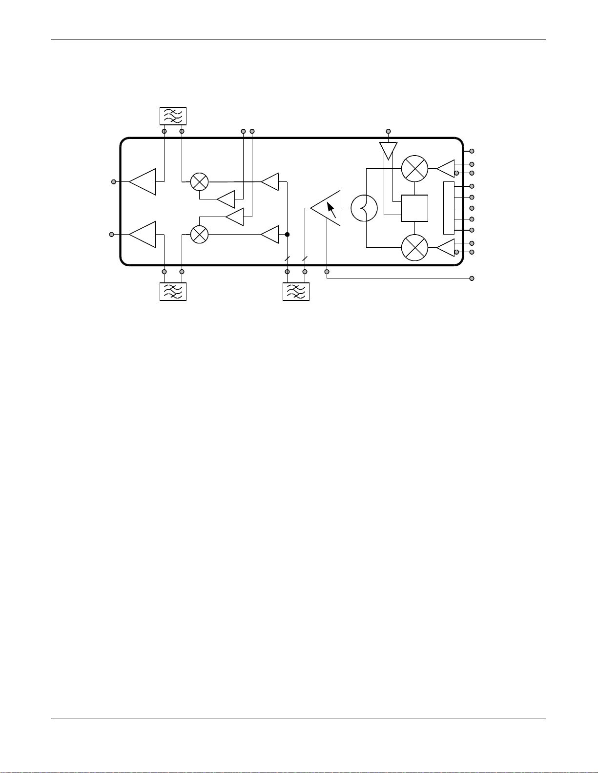
Technical Description
The CX74037 is a TDMA transmitter for the 800 MHz and 1900
MHz bands. It also can be used as an FM transmitter in AMPS
mode at the 800 MHz band. A band select command chooses
between the 800 MHz band and the 1900 MHz band. A mode
select command chooses between TDMA and AMPS mode.
The chip consist of an I/Q modulator, IF LO input buffer, IF VGA,
two upconverters for the 800 MHz and 1900 MHz bands, and
two PA drivers for the 800 MHz and the 1900 MHz bands.
I/Q Modulator
signal to an IF signal using one of the two local oscillator inputs.
This signal is fed directly to the VGA amplifier.
Variable Gain Amplifier
receives its signal from the I/Q modulator, amplifies it, and then
is taken off-chip to be filtered before routing it to the
upconverter. A dynamic range of 90 dB is available on the
amplifier. A DC voltage of 0.2 to 2.5 V is needed to control the
gain of the amplifier.
Upconverters
receive the IF signal from the VGA amplifier. Each upconverter
requires an external LO controlled by an external Phase Locked
Loop (PLL). The band select command switches between the
800 MHz and the 1900 MHz bands.
. The I/Q modulator converts the incoming I/Q
. The VGA is a differential amplifier that
. The 800 MHz and 1900 MHz upconverters
CX74037
TX RFIC
2 2
LPF or BPF
IF LO IN
VCC
I Data
IF Select
Band Select
PULL En
PA Driver En
Interface
VGA En
Q Data
Vvga
101103A-2_080900
PA Drivers
÷ 2
. Two PA drivers are included, the 800 MHz driver
and the 1900 MHz driver. Each driver takes its input from the
upconverter after passing through an image rejection filter. The
driver amplifies the signal and sends it to an external PA.
Electrical and Mechanical Specifications ________________
The signal pin assignments and functional pin descriptions are
found in Table 1. The absolute maximum ratings of the
CX74037 are provided in Table 2, the recommended operating
conditions are specified in Table 3. Electrical characteristics for
the CX74037 are shown in Table 4. Table 5 defines the control
signal logic.
Figure 3 provides the package dimensions for the 48-pin, 7x7
LGA package.
ESD Sensitivity
The CX74037 is a static-sensitive electronic device. Do not
operate or store near strong electrostatic fields. Take proper
ESD precautions.
Data Sheet
Conexant Proprietary
Data Subject to Change September 27, 2000
Doc. No. 101103A
Page 3

Transmit RF IC for TDMA or AMPS Applications CX74037
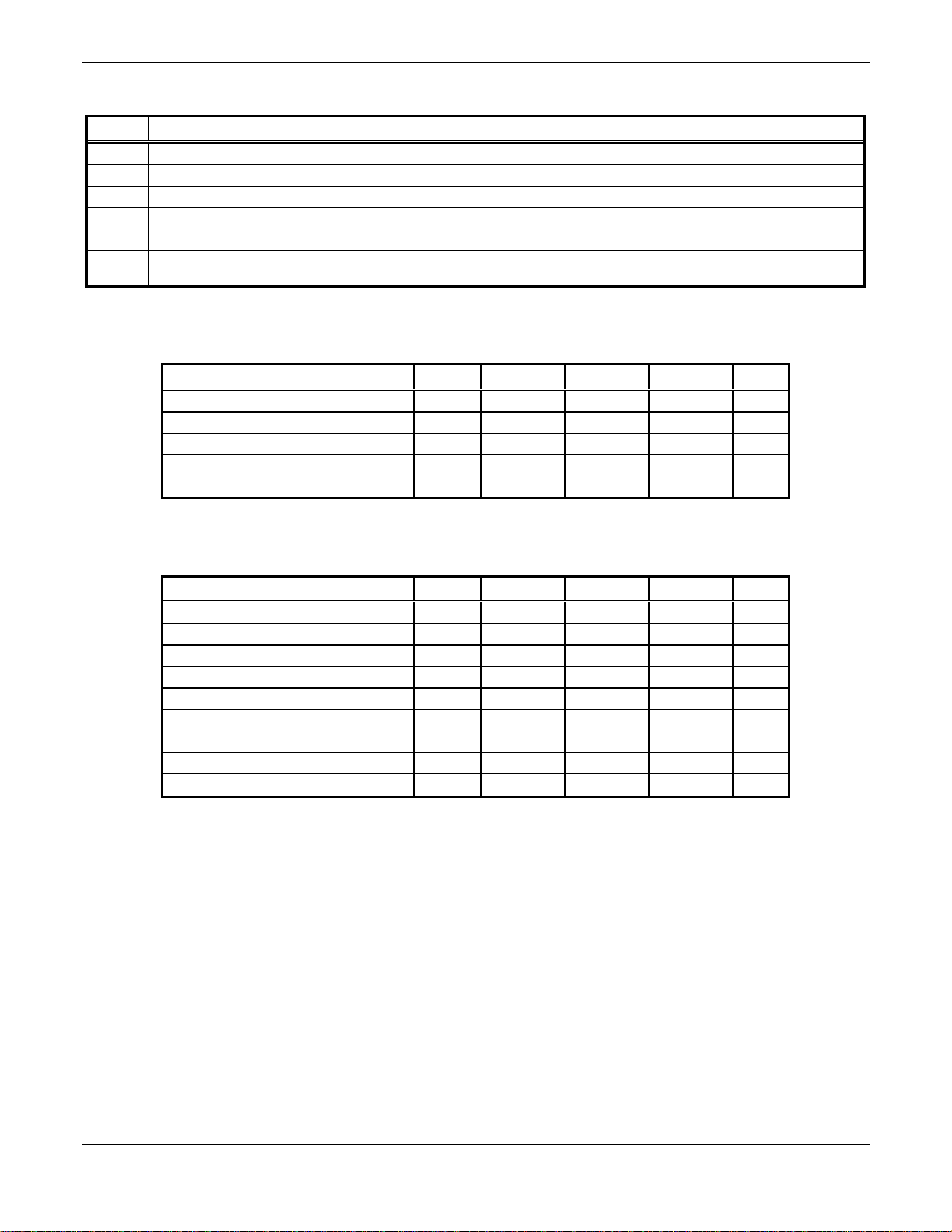
Table 1. CX74037 Signal Definition (1 of 2)
Pin NO. Name Description
1 Mix_IN+ Input to RF Upconverters. Internally AC c oupled, high impedance.
2 Mix_IN- Input to RF Upconverters. Internally AC c oupled, high impedance.
3 VCC_IF Supply volta ge for the AGC amplifier.
4 VGA_GC The input pin f or AGC gain control. A DC contr ol voltage should be applied to this pin to vary the gain of the IF amplifier.
5 VGA_OUT- VGA Output, open collector. External resistive (300 ohms ) pull up to Vcc required.
6 VGA_OUT+ VGA Output, open c ollector. External resisti ve (300 ohms) pull up to Vcc required.
7 VCC_LD_PC S Supply voltage for the PCS l ast stage driver amplifier.
8 POT_CELL This pin is connected to an external resistor. The value of the resistor will vary the bias current of the cellular driver.
9 DRV_ENA
10 RF_PCS_OUT Output pin for t he PCS driver amplifier. Impedance matching is required.
11 VCC_BIAS Supply voltage of bias cells.
12 RF_CELL_OUT Output pin for the cellular driver amplif ier. Impedance matching is required.
13 BAND This is a control signal input pin. It selects between cell ular band and PCS band. When the input is low, the cellular band is chosen.
14 VCC_DRV_CEL Supply voltage for the driver of the c ellular band.
15 POT_PCS This pin is connected to an external resistor. The value of the resistor will vary the bias current of the PCS driver.
16 VCC_MID_PCS Supply voltage for the f irst amplifier in the PCS driv er block.
17 DRV_CELL_IN The Cellular driver amplifier input pin. Impedance matching is required.
18 DRV_PCS_IN The PCS driver amplifier input pin. Impedance matching i s required.
19 I_DATA+ The baseband input for I channel. This is a balanced input. A DC bias has to be supplied t o the pin.
20 I_DATA- Same as pin 20, except complement ary input. This pin should be pul l low (0 V) in FM mode.
21 VCC_MOD Supply voltage for the I/Q modulator.
22 Q_DATA+ The baseband input for Q channel. This i s a balanced input. A DC bias has to be supplied to the pin.
23 Q_DATA- Same as pin 23, except complementary input.
24 NC There is no connection on thi s pin. Should be tied to ground.
25 NC There is no connection on thi s pin. Should be tied to ground.
26 NC There is no connection on thi s pin. Should be tied to ground.
27 MIX_PCS_OUT Output of the P CS upconverter. Impedance matching required.
28 VCC_DIFF_DRV Supply volta ge for a differential amplifier in the upconverter block.
29 PULL_ENA This is a control signal input pin. When the input is low, the IF VCOs, RF Mixer and buffers, and div ide by 2 sections will be
30 MIX_CELL_OUT Output of the Cellular upconverter. Impedance matching requi red.
31 VCC_DIV Supply volta ge for the dividers and VCO buffer.
32 NC There is no connection on thi s pin. Should be tied to ground.
33 NC There is no connection on thi s pin. Should be tied to ground.
34 NC There is no connection on thi s pin. Should be tied to ground.
35 IF VCO IN1+ Input pin for the modulator LO signal. The frequency is 2xIF. Can be used single-ended. AC ground the unused pin.
36 IF VCO IN1- Input pin for the modulator LO signal. The frequency is 2xIF. Can be used single-ended. AC ground the unused pin.
37 NC There is no connection on thi s pin. Should be tied to ground.
38 NC There is no connection on thi s pin. Should be tied to ground.
39 MODE This is a control signal input pin. When the i nput is low, the AMPS mode is selected. If the input is high, T DMA mode is selected. FM
40 IF VCO IN2+ Input pin for the modulator LO signal. The frequency is 2xIF. Can be used single-ended. AC ground the unused pin.
41 IF VCO IN2- Input pin for the modulator LO signal. The frequency is 2xIF. Can be used single-ended. AC ground the unused pin.
42 IF_SELECT Control signal to select IF VCO INPUT1 or INPUT2. “1” will select IF VCO INPUT1 and “0” will select IF VCO INPUT2.
This is the input pin for the upconverter a nd the driver control signal. When the pin is low the driver and the upconverter are
deactivated.
When the input is high, the PCS band is chosen.
disabled. When the input is high, the mentioned sections will be enabled.
output is 9 dB hi gher at the modulator output .
101103A
Conexant – Proprietary
September 27, 2000 Data Subject to Change
3
Page 4
CX74037 Transmit RF IC for TDMA or AMPS Applications
Table 1. CX74037 Signal Definition (2 of 2)
Pin No. Name Description
43 NC Connect to gro und.
44 NC Connect to gro und.
45 LO_PCS_IN This is the input pin for the local oscillator for the PCS band. It is internally matched.
46 VCC_MIX Supply volta ge for the mixer in the upconverter block and for the LO buffer .
47 LO_CELL This is the input pin for the local oscillator for the cellular band. It is internally matched.
48 VGA_EN This is a control signal input pin. When the input is low, the VGA and I/Q Modulator sections will be disabled. When the input is high,
the mentioned sections will be enabled.
Table 2. Absolute Maximum Ratings
Parameter Symbol Minimum Typical Maximum Units
Supply voltage VCC –0.3 +5.0 V
Input voltag e range –0.3 VCC V
Power dissipation 600 mW
Ambient operat ing temperature –30 +80 °C
Storage temperature –40 +125 °C
Table 3. CX74037 Recommended Operating Conditions
Parameter Symbol Minimum Typical Maximum Units
Supply volta ge 2.7 3. 0 3.6 V
Logic level high 1.9 V
Logic level low 0.8 V
Supply current in 800 MHz TDM A @ 7 dBm 75 mA
Supply current in 800 MHz AMP S @ 7 dBm 75 mA
Supply current in 800 MHz (DRV_ENA off) 45 mA
Supply current in 1900 MHz TD MA @ 8.0 dBm 84 mA
Supply current in 1900 MHz TDMA (DRV_ENA off ) 48 mA
Supply current in sleep mod e 20
µ
A
4
Conexant – Proprietary
101103A
Data Subject to Change September 27, 2000
Page 5

Transmit RF IC for TDMA or AMPS Applications CX74037
Table 4. CX74037 Electrical Characteristics (1 of 3)
VCC = 3.0 V, T
A
= 25 oC, PLO = –10 dBm, input externally matched
Parameter Symbol Test Conditions Min Typical Max Units
IF VCO Input
Input freque ncy range (2X IF frequency) 100 640 MHz
Input signal level –10 –3+3dBm
I/Q Modulator (Output Not Measurable)
Input voltage level, differential 1.4 Vp-p
Common mode input voltage level 1.4 1.85 2.1 V
Input DC offset 4mV
Input impedance 100K
Gain variation over process, temperature,
VCC
I/Q gain mismatch 0.3 0.4 dB
I/Q phase imbalance 2 4 degrees
0.4 dB
Ω
Transmit VGA
VGA frequency range (–1 dB bandwidth) 50 320 MHz
VGA gain (with a 600 Ω differential load):
Maximum
Minimum
VGA gain variation with VCC 3.0 to 3.6 V @
VCTRL 2 V
Gain variatio n with temperat ure –1.0 +1.0 dB
Gain control input impedance 40K
VGA gain slope 45 50 55 dB/V
VGA gain control range 0.5 2.5 V
Gain slope var iation over any 6 dB segment –3+3dB/V
Output power level @ 20 dB gain –13 dBm
P1dB @ 22 dB gain –3dBm
NF @ 22 dB gain 6dB
NF at -52 dB gain 52 53 dB
Operating temperature range –30 +25 +80
22
–64
–3+3dB
24
–62
26
–60
dB
dB
°
Ω
C
Cellular Upconverter
LO frequency range 1017 1043 MHz
LO input return loss (reference to 50 Ω)
Output frequ ency 824 849 MHz
Output return loss from 824 MHz to 849 MHz
(reference to 50 Ω)
Conversion gai n 7 8 9 dB
Gain degradat ion @ VCC 2.7 V 0.1 dB
ACPR in 30 kHz at 30 kHz offset @ –5 dBm
output; cascaded
ACPR in 30 kHz at 60 kHz offset @ –5 dBm
output; cascaded
–10 dB
–15 dB
–33 dBc
–56 dBc
101103A
Conexant – Proprietary
September 27, 2000 Data Subject to Change
5
Page 6

CX74037 Transmit RF IC for TDMA or AMPS Applications
Table 4. RF150 Electrical Characteristics (2 of 3)
DD
V
= 2.7 V, –40 oC < T
A
< +85 oC, unless specified
Parameter Symbol Test Conditions Min Typical Max Units
Cellular Upconverter (continued)
Output P1dB 2 3 dBm
Noise figure @ 8 dB gain 12 13 dB
LO to RF leakage @ maximum gain,
LO = –10 dBm
Operating temperature range –30 +25 +80
–35 dBm
°
C
PCS Upconverter
LO frequency range 2078 2139 MHz
LO input return loss (reference to 50 Ω)
Output frequ ency 1850 1910 MHz
Conversion gai n 8 9 10 dB
ACPR in 30 kHz at 30 kHz offset @ –4 dBm
output; cascaded
ACPR in 30 kHz at 60 kHz offset @ –4 dBm
output; cascaded
Noise figure @ 9 dB gain 910dB
P1dB 0dBm
LO to RF leakage @ maximum gain,
LO = –15 dBm
Operating temperature range –30 +25 +80
–10 dB
–33 dBc
–57 dBc
–35 dBm
°
C
Cellular PA Driver
Output frequ ency 824 849 MHz
Gain 13 14 15 dB
Output power l evel @ 14 dB gain 7 dBm
Input return loss (reference to 50 Ω)
Output P1dB 14.5 dBm
ACPR in 30 kHz band at 30 kHz offset @ 7
dBm output; c ascaded
ACPR in 30 kHz band at 60 kHz offset @ 7
dBm output; c ascaded
Output return loss (reference to 50 Ω)
Noise figure 68dB
Operating temperature range –30 +25 +80
External bias resistor value for +14.5 dBm
P1dB
–15 dB
–32 dBc
–55 dBc
–15 dB
°
120
Ω
C
6
Conexant – Proprietary
101103A
Data Subject to Change September 27, 2000
Page 7

Transmit RF IC for TDMA or AMPS Applications CX74037
Table 4. RF150 Electrical Characteristics (3 of 3)
DD
V
= 2.7 V, –40 oC < T
A
< +85 oC, unless specified
Parameter Symbol Test Conditions Min Typical Max Units
PCS PA Driver
Input return loss (reference to 50 Ω)
Output frequ ency 1850 1910 MHz
Gain 15 16 17 dB
Output power l evel @ 16 dB gain 8.0 dBm
Output P1dB 14 dBm
ACPR in 30 kHz band at 30 kHz offset @ 8.0
dBm output; c ascaded
ACPR in 30 kHz band at 60 kHz offset @ 8.0
dBm output; c ascaded
Output return loss (reference to 50 Ω)
Noise figure 910dB
Operating temperature range –30 +25 +80
External bias resistor value for +16 dBm of
P1dB
–15 dB
–32 dBc
–55 dBc
–15 dB
°
130
Ω
C
Table 5. Control Signal Truth Table
Signal Name Logic 1 Logic 0 Remark
VGA_ENA ON OFF
DRV_ENA ON OFF Cell and PCS band
BAND PCS Cell
PULL_ENA ON OFF IF VCO, RF mixer buffers, divide-by-2
IF_Select IF VCO IN1 IF VCO IN2
MODE TDMA FM In FM mode:
Normal DC bias on I+,
0 V bias on I–
101103A
Conexant – Proprietary
September 27, 2000 Data Subject to Change
7
Page 8

CX74037 Transmit RF IC for TDMA or AMPS Applications
Pin 1
7.00 – 0.10
1.20 – 0.10
0.30 – 0.05
7.00 – 0.10
Top View
Side View
0.300 – 0.05
Mold
Substrate
0.355 – 0.05
3.450
Bottom View
Pin 1
indication
Solder Mask
Exposed Metal
R2.225
3.450
0.500
All dimensions are in millimeters
C924
Figure 3. CX74037 Package Dimensions for a 48-Pin, 7x7 LGA Package
8
Conexant – Proprietary
101103A
Data Subject to Change September 27, 2000
Page 9

Transmit RF IC for TDMA or AMPS Applications CX74037
Ordering Information
Model Name
Transmit RF IC CX74037
Manufacturing Part
Number
101103A
September 27, 2000 Data Subject to Change
Conexant – Proprietary
9
Page 10

© 2000, Conexant Systems, Inc. All Rights Reserved.
Information in this document is provided i n connection with Conexant Systems, Inc. ("Conexant ") products. These materials are provid ed by Conexant as a service to its
customers and may be used for informational purposes only. Conexant assumes no responsibility for errors or omissions in these materials. Conexant may make changes to
specifications and product descriptions at any time, without notice. Conexant makes no commitment to update the information and shall have no responsibility whatsoever for
conflicts or incompatibilities arising from future changes to its specifications and product descriptions.
No license, ex press or impli ed, by estoppe l or otherwis e, to any intellectual property rights is granted by this document. Exc ept as provid ed in Conexant’s Terms and
Conditions of Sale for such products , Conexant assum es no liability whatsoever.
THESE MATERI ALS ARE PROVIDED "AS IS" WITHOUT WARRANTY OF ANY KIND, EITHER EXPRESS OR IMPLIED, RELATING TO SALE AND/OR USE OF
CONEXANT PRODUCTS INCLUDING LIABILITY OR WARRANTIES RELATING TO FITNESS FOR A PARTICULAR PURPOSE, CONSEQUENTIAL OR INCIDEN TAL
DAMAGES, MERCHANTABILITY, OR INFRINGEMENT OF ANY PATENT, COPYRIGHT OR OTHER INTELLECTUAL PROPERTY RI GHT. CONEXANT F URTHER DOES
NOT WARRANT THE ACCURACY OR COMPLETENESS OF THE INFORMATION, TEXT, GRAPHICS OR OTHER ITEMS CONTAINED WITHIN THESE MATERIALS.
CONEXANT SHALL NOT BE LIABL E FOR ANY SPECIAL, INDIRECT, INCIDENTAL, OR CONSEQUENTIAL D AMAGES, INCLUDING WITHOUT LI MITATION, LOST
REVENUES OR LOST PROFITS, WHI CH MAY RESULT FROM THE USE OF THESE MATERIALS.
Conexant products are not i ntended for use in medical, lifesaving or life sustaining applications. Conexant customers usi ng or selling Conexant products for use in such
applications do so at their own risk and agree to fully indemnify Conexant for any damages resulting from such i m proper use or sale.
The following are trademarks of Conexant Systems, Inc.: Conexant™, the Conexant C s ymbol, and “What’s Next in Comm unications Tec hnologies”™. Pr oduct names or
services l isted in this publi cation are for identification purposes only, and may be trademarks of third parties. Third-party brands and names are the property of their
respective owners.
Additional information, p osted at www.conexant.com , is incorpor ated by reference.
Reader Respo nse: Conexant strives to pr oduce quality documentation and welcomes your feedback. Please send comments and s uggestions to tech.pubs@conexant.com.
For technical questions, contact your l ocal Conexant sales office or field applic ations engineer.
Page 11

Further Information
literature@conexant.com
(800) 854-8099 (North
America)
(949) 483-6996 (International)
Printed in USA
World Headquarters
Conexant Systems, Inc.
4311 Jamboree Roa d
Newport Beach, CA
92660-3007
Phone: (949) 483-4600
Fax 1: (949) 483-4078
Fax 2: (949) 483-4391
Americas
U.S. Northwest/
Pacific Northwest – Santa Clara
Phone: (408) 551-0270
Fax: (408) 249-7113
U.S. Southwest – Los Angeles
Phone: (949) 483-9119
Fax: (949) 483-9090
U.S. Southwest – Orange County
Phone: (949) 483-9119
Fax: (949) 483-9090
U.S. Southwest – San Diego
Phone: (858) 713-3374
Fax: (858) 713-4001
U.S. North Central – Illinois
Phone: (630) 773-3454
Fax: (630) 773-3907
U.S. South Central – Texas
Phone: (972) 733-0723
Fax: (972) 407-0639
U.S. Northeast – Massachusetts
Phone: (978) 367-3200
Fax: (978) 256-6868
U.S. Southeast – North Car oli na
Phone: (919) 858-9110
Fax: (919) 858-8669
U.S. Southeast – Florida/
South America
Phone: (727) 799-8406
Fax: (727) 799-8306
U.S. Mid-Atlantic – Pennsylvania
Phone: (215) 244-6784
Fax: (215) 244-9292
Canada – Ontario
Phone: (613) 271-2358
Fax: (613) 271-2359
Europe
Europe Central – Germany
Phone: +49 89 829-1320
Fax: +49 89 834-2734
Europe North – England
Phone: +44 (0)118 920 9500
Fax: +44 (0)118 920 9595
Europe – Israel/Greece
Phone: +972 9 9524000
Fax: +972 9 9573732
Europe South – France
Phone: +33 1 41 44 36 51
Fax: +33 1 41 44 36 90
Europe Mediterranean – Italy
Phone: +39 02 93179911
Fax: +39 02 93179913
Europe – Sweden
Phone: +46 (0) 8 5091 4319
Fax: +46 (0) 8 590 041 10
Europe – Finland
Phone: +358 (0) 9 85 666 435
Fax: +358 (0) 9 85 666 220
Asia – Pacific
Taiwan
Phone: (886-2) 2-720-0282
Fax: (886-2) 2-757-67 60
Australia
Phone: (613) 9583 2650
Fax: (613) 9583 9453
China – Central
Phone: 86-21-6361-2515
Fax: 86-21-6361-2516
China – South
Phone: (852) 2 827-0181
Fax: (852) 2 827-6488
China – South (Satellite)
Phone: (86) 755-518- 2495
China – North
Phone: (86-10) 8529-9777
Fax: (86-10) 8529-9778
India
Phone: (91-11) 341 2216
Fax: (91-11) 341 2217
Korea
Phone: (82-2) 565-2880
Fax: (82-2) 565-1440
Korea (Satellite)
Phone: (82-53) 745- 2880
Fax: (82-53) 745-1440
Singapore
Phone: (65) 737 7355
Fax: (65) 737 9077
Japan
Phone: (81-3) 5371 1520
Fax: (81-3) 5371 1501
www.conexant.com
 Loading...