

Page 1
CX74036
IS-136 Receive RF IC for TDMA and AMPS Applications
Conexant’s CX74036 receive RF IC is an advanced, highly integrated and high
performance, triple-mode, dual-band IC for IS-136 compliant cellular radio
applications and is designed in an advanced 28 GHz Ft BiCMOS process. In the
800 MHz cellular band, the CX74036 is designed to operate in both the Time
Division Multiple Access (TDMA) mode and Advanced Mobile Phone System
(AMPS) mode. In the 1900 MHz Personal Communications System (PCS) band,
the device operates in the TDMA mode.
The CX74036 embodies all the necessary functions for a radio receiver system
except for the RF and Intermediate Frequency (IF) filters and RF Local Oscillator
(LO) sources. The device front-end section has two Low Noise Amplifier (LNA) and
mixer pairs, one for the 800 MHz band and the other for the 1900 MHz band. A
common path is taken from the first IF mixer output to the demodulator output.
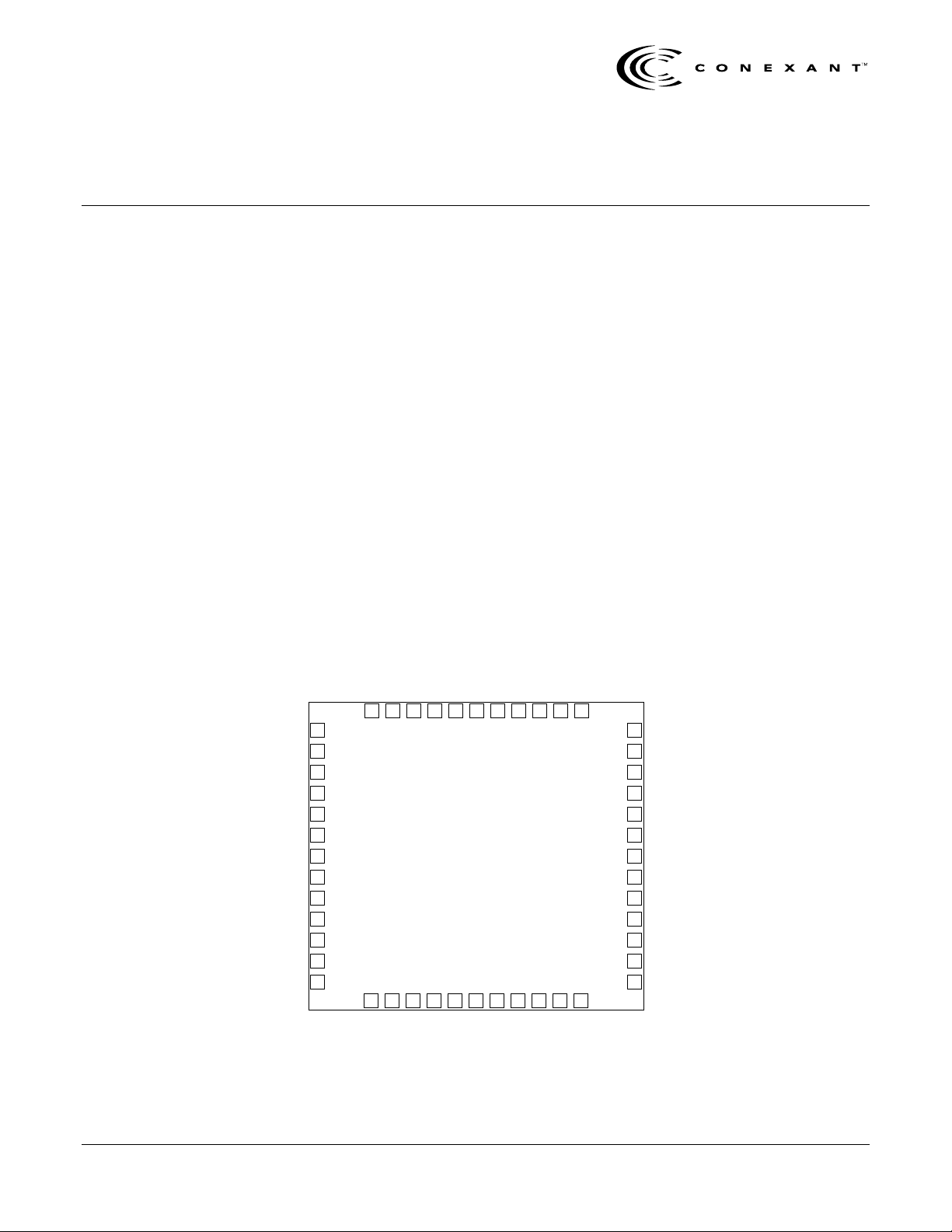
The CX74036 48-pin, 7x7 Land Grid Array (LGA) package pin configuration is
shown in Figure 1. A block diagram of the CX74036 is shown in Figure 2.
LNA_OH
LNA_OL
VCC2_LNAH
VCC2_LNAL
VCC1_LNA
NC2
LNA_INL
LNA_INH
NC1
Features
• Front-end to baseband in one IC
• Inphase and Quadrature (I/Q) demodulator
• 3 V supply operation
• Low current consumption
• LNA gain switch with current reduction
• IF LO synthesizer with Voltage Controlled
Oscillator (VCO) (requires external tank)
• 70 dB Variable Gain Amplifier (VGA) dynamic
range
• Low Noise Figure (NF) and high 3rd order Input
Intercept Point (IIP3) mixers
Applications
• Cellular and/or PCS band phones
• TDMA and/or AMPS mode phones
• Portable battery powered radio equipment
EXT_LO
IF_O +
Data Sheet
LNA_G
MXIH
MIXIL
BAND
CHIP_EN
LOIH
LOIL
VCC_MX
STANDBY
IQ/IF
MXOUT+
MXOUT-
MX2I+
1
2
3
4
5
6
7
8
9
10
11
12
13
MX2I-
45464748 44 43 42 41 40 39 38
17161514 18 19 20 21 22 23 24
Vvga
VCC_IF
MX2OUT
IFBYPASS
VGAI-
VCC_VGA
VGAI+
FB_CAP
37
36
35
34
33
32
31
30
29
28
27
26
25
CLK
LATCH_EN
101105A-1_082500
Figure 1. CX74036 48-Pin, 7x7 LGA Package Pin Configuration
Conexant – Proprietary
Data Subject to Change October 17, 2000
IF_O Q-
Q+
I-
I+
EXT_LOIN
VCC_VCO
VCO-
VCO+
VCC_SYN
LP_FIL
REFIN
DATA
Doc. No. 101105A
Page 2
CX74036 Receive RF IC
Image Rejection Filter
PCS RF InCell RF In
CX74036
RX RFIC
Cell LO
Image Rejection Filter
1st IF S A W
PCS LO
450 KHz
1st IF L O
÷P
VHF
Synth
19.44 MHz Ext.1.8 MHz
Power
Management
÷ 4
IF Bu ffe r
Vvga
Vcc
Standby
CLK
DATA
EN
LNA Gain
Interface
101105A-2_101200
Band Select
Power Down
VCO/REFIN
I
IQ/
IF
Q
IF Ou t
Figure 2. CX74036 Functional Block Diagram
Technical Description
Low Noise Amplifiers:
independent LNAs for the cellular and PCS bands. The gain of
both LNAs can be switched off to a loss mode via one command
line interface. Only one LNA is powered at any given time.
Control is done by an external band-select control signal. The
input and output matches are external to the chip. The LNAs’
parameters, Noise Figure (NF), and gain are chosen to provide
an excellent balance between system sensitivity and IIP3
requirements to achieve maximum dynamic range. Both LNA
outputs are ported off-chip to allow for image filtering before
being fed to the RF mixer inputs.
RF Mixers:
The mixers are designed to operate with a low LO
input power level of –10 dBm. This eliminates the requirement of
buffer amplifiers for the external VCO. Cellular band mixer high
gain and low NF performance allow for the cellular LNA gain to
be lower, which saves current consumption. Both mixers are
designed to provide high suppression of one-half IF response.
The outputs of both mixers share a common interface path to
the external IF Surface Acoustic Wave (SAW) filter, which
reduces complexity and cost. The RF mixer load configuration is
shown in Figure 3. Inductors can be Surface Mount Multilayer
Chip (SMMC) components.
First IF Mixer
: This mixer begins the common signal path for
both cellular and PCS band modes. Input and output impedance
are set to values that are close to the most commonly available
SAW and ceramic filters.
The CX74036 contains two
Vcc
330 nH
1200 pF
+
RF Mixers
Output
10 K
Ω
to IF S A W
Filter
-
330 nH
Vcc
Figure 3. RF Mixer Load Configuration
Variable Gain Amplifier:
dynamic range to satisfy the high system dynamic range
requirement. With the inclusion of the LNA gain switch, the
system dynamic range is extended to more than 95 dB.
I/Q Demodulator:
Using digital circuitry generates a stable
quadrature LO signal, on-chip direct connection to the VGA
output, on-chip LO source, and lowpass filtering for each
channel. This, in turn, provides a high performance I/Q
demodulator with very low amplitude and phase offsets. The
output signal quality is compatible with many baseband interface
requirements.
1200 pF
101105A-3_101100
The VGA itself provides 70 dB of
2
Conexant – Proprietary
101105A
Data Subject to Change October 17, 2000
Page 3
Receive RF IC CX74036
VHF Synthesizer and Oscillator:
The on-chip VHF synthesizer
and an oscillator with an added external tank circuit generate
the required second IF LO signal for conversion down to the
standard second IF signal. A programmable divide circuit is also
included to generate the LO for the I/Q demodulator. Depending
on the frequency plan used, an option is provided to inject an
external LO source for the I/Q demodulator.
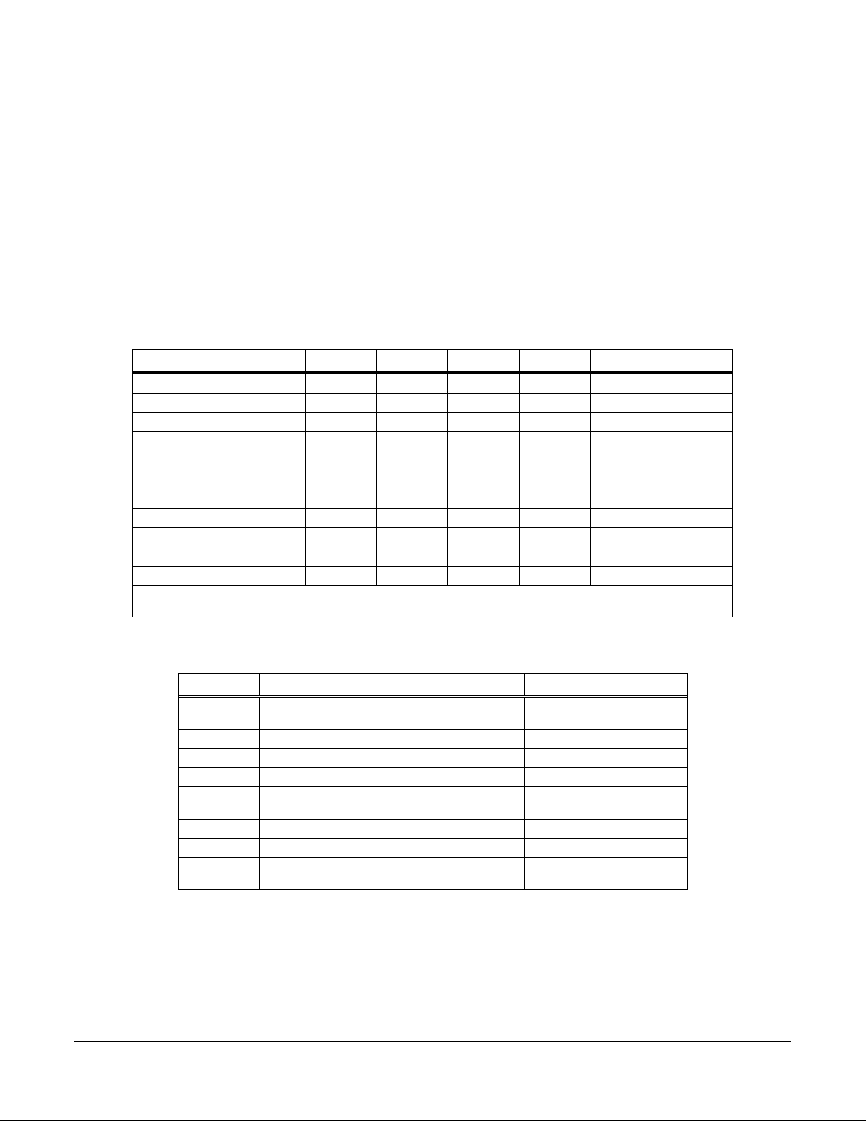
Control Logic Truth Table.
The Control Logic Truth Table is
shown in Table 1.
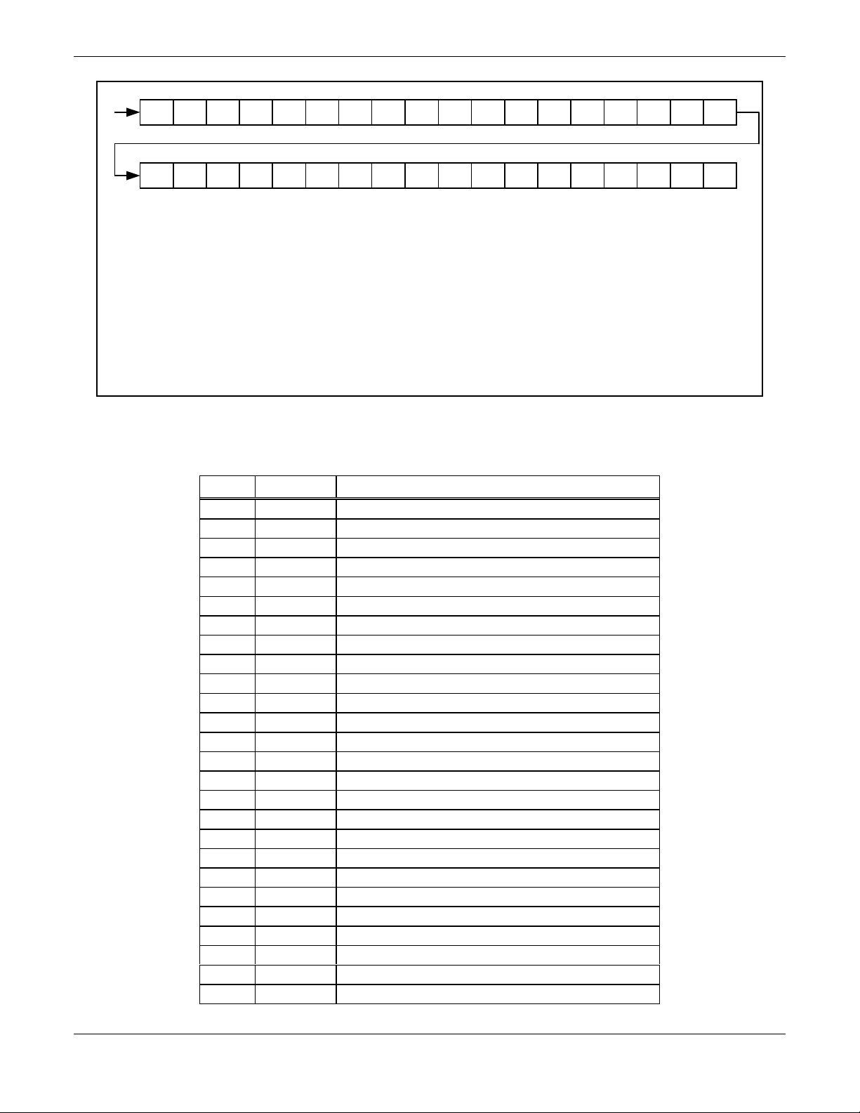
3-Wire Bus Programming.
The 3-wire bus programming data
is included in Table 2. The 3-wire programming data pattern
diagram is shown in Figure 4.
Table 1. Control Logic Truth Table
Mode LNA_G BAND CHIP_EN STANDBY IQ/IF LO_EXT
Active, Low Band, LNA High Gain, IQ101101
Active, High Band, LNA High Gain, IQ111101
Active, Low Band, LNA Low Gain, IQ001101
Active, High Band, LNA Low Gain, IQ011101
Active, Low Band, LNA High Gain, IF101111
Active, High Band, LNA High Gain, IF111111
Active, Low Band, LNA Low Gain, IF001111
Active, High Band, LNA Low Gain, IF011111
Standby --- --- 0 1 --- 1
External LO Mode --- --- 1 --- --- 0
Sleep --- --- 0 0 --- 0
Note.
Synthesizer prescaler and charge pump can be turned off via programming from the 3-wire bus. This mode can be used when driv i ng
the IF Mixer with an external synthesizer.
Electrical and Mechanical Specifications ________________
The signal pin assignments, names, and descriptions are found
in Table 3. Absolute maximum ratings are provided in Table 4,
the recommended operating conditions are specified in Table 5.
Electrical characteristics are shown in Table 6.
Figure 6 provides the 48-Pin, 7x7 LGA package dimensions.
ESD Sensitivity
The CX74036 is a static-sensitive electronic device. Do not
operate or store near strong electrostatic fields. Take proper
ESD precautions.
Table 2. 3-Wire Bus Programming Data
Bit Number Function Programming
00 Select VCO or Reference Input to Programming Counter “0” = Reference Input
01 – 08 Synthesizer M Counter Programming, MB0 – MB7
09 – 12 Synthesizer A Counter Programming, AB0 – AB3
13 – 23 Synthesizer Reference C ounter Programming, RB0 – RB10
24 Charge Pump P olarity “0” = Ground Referenced Varactor
25 – 32 Programmable M Counter Programming, M2B0 – M2B1
33 – 34 Programmable A Counter Programming, A2B0 – A2B1
35 Synthesizer Power down (For External Synt hesizer Mode) “0” = Internal Synthesizer
101075A
October 17, 2000 Data Subject to Change
Conexant – Proprietary
“1” = VCO Input
“1” = VCC Referenced Varactor
“1” = External Synthesizer
3
Page 4
CX74036 Receive RF IC
MSB
SPD
35
34
A2B033M2B732M2B631M2B5
A2B1
30
M2B4
29
28
M2B227M2B126M2B025CPP
M2B3
24
RB10
23
22
RB821RB720RB619RB5
RB9
18
RB4
17
16
RB215RB114RB013AB3
RB3
12
AB2
11
10
AB009MB708MB607MB5
AB1
06
05
MB4
04
MB203MB102MB001VRS
MB3
00 = First bit shifted in (LSB)
35 = Last bit shifted in (MSB)
VRS = Select VCO or Reference Input to Programmable Counter
"0" = Reference Input
"1" = VCO Input
MB0 - MB 7: Programming for Synthesizer M Counter: MB0 (LSB), MB7 = (MSB)
AB0 - AB3: Programming for Synthesizer A Counter: AB0 (LSB), AB7 = (MS B)
RB0 - RB10: Programming for Synthesizer R Counter: RB0 (LSB), RB10 = (MSB ). CPP = Change P um p Polarity,
"0" = G rou nd R efe ren ce
M2B0 - M2B7: Programming for LO Divider M Counter: M2B0 (LSB), M2B7 = (MSB)
A2B0 - A2B7: Programming for LO Divider A Counter: A2B0 (LSB), A2B1 = (MSB)
SPD = Sy nthesizer Power Down (for External Synthesizer Mode)
"1" = Inte rnal S y n the siz er,
"0"= E x terna l S yn the s ize r
101105A-4_101200
Figure 4. 3-Wire Programming Data Pattern
Table 3. Signal Pin Names and Definitions (1 of 2)
Pin No. Signal Name Description
1 LN A_G LNAs gain control command
2 MXIH 1900 MHz band mixer Input
3 MIXIL 800 MHz band mix er Input
4 BAND 800 MHz/1900 MHz band select command
5 CHIP_EN Chip power down select command
6 LOIH 1900 MHz RF mixer LO input
7 LOIL 800 MHz RF mixer LO input
8VCC_MX RF mixer VCC
9 ST ANDBY Control signal to enable RF LO buffers and VHF synthesi zer
10 IQ/IF I/Q or IF output select command
11 MXOUT+ RF mixer output. Open Collector.
12 MXOUT- RF mixer output. Open Collector.
13 MX2I+ IF mixer input
14 MX2I- IF mixer input
15 VCC_IF IF section VCC
16 IFBYPASS IF mixer bias decoupling
17 MX2OUT IF mixer output
18 Vvga Analog volta ge input for VGA gain control
19 VCC_VGA VGA section VCC
20 VGAI- VGA input
21 VGAI+ VGA input
22 FB_CAP VGA DC feedback fil ter capacitor c onnection
23 LATCH_EN Enable input lin e for internal synthesizer programming
24 CLK Serial clock input line for internal synthesizer programming
25 DATA Serial data input line for internal synt hesizer programming
26 REFIN 19.44 MHz reference oscillator input. Requires VCC/2 DC bias.
LSB
00
4
Conexant – Proprietary
101105A
Data Subject to Change October 17, 2000
Page 5

Receive RF IC CX74036
Table 3. Signal Pin Names and Definitions (2 of 2)
Pin No. Signal Name Description
27 LP_FIL IF PLL exter nal loop filter connection
28 VCC_SYN Synthesizer secti on VCC
29 VCO+ IF VCO external tank circui t connection
30 VCO- IF VCO external tank circuit connectio n
31 VCC_VCO VCO section VCC
32 EXT_LOIN External LO input for quadrature detector. Requires VCC/2 DC bias.
33 I+ I Channel data output
34 I– I Channel data output
35 Q+ Q Channel data output
36 Q– Q Channel data output
37 IF_O– Buffered IF output
38 IF_O+ Buffered IF output
39 EXT_LO Programmable counter ON/OFF control signal for choosing between
40 NC1 No connect
41 LNA_INH 1900 MHz band LNA input
42 LNA_INL 800 MHz band LNA input
43 NC2 No connect
44 VCC1_LNA Bias VCC for LNAs
45 VCC2_LNAL VCC for cellular band LN A.
46 VCC2_LNAH VCC for PCS band LN A.
47 LNA_OL 800 MHz band LNA output. Requires external matching and AC coupling.
48 LNA_OH 1900 MHz band LNA output. Requires external mat ching and AC coupling.
Internal and External demodulator LO.
Table 4. Absolute Maximum Ratings
Parameter Symbol Minimum Typical Maximum Units
Supply volta ge VCC –0.3 +3.6 V
Input voltag e range –0.3 VCC V
LNA input power +5 dBm
Power dissipation 600 mW
Ambient operat ing temperature –40 +85 °C
Storage temperature –40 +125 °C
101105A
Conexant – Proprietary
October 17, 2000 Data Subject to Change
5
Page 6

CX74036 Receive RF IC
Table 5. Recommended Operating Conditions
Parameter Symbol Minimum Typical Maximum Units
Supply volta ge 2.7 3.0 3.6 V
Logic level high 1.9 V
Logic level low 0.8 V
Supply curre nt in cellular TDMA/AMPS, high gain 30 mA
Supply current in cellular TDMA/AMPS, low gain 28 mA
Supply curre nt in PCS TDMA, high gain 33 mA
Supply current in PCS TDMA, low gain 30 mA
Supply curre nt in cellular I F, high gain 29 mA
Supply curre nt in PCS IF, high gain 32
Supply current in sleep mode TBD
µ
A
Table 6. Electrical Characteristics (1 of 5)
LNA 800
MIX 800
A
= 25 oC
2
15
9
8
–15
91011dB
14
13
16
–15
≥
0/ ≥ –25
10 dBm
TBD
50
≥
30/ ≥ –15
8.5 9.0
15 dBm
450
2.3
2.75
20
17 dB
10
dB
dBm
Ω
Ω
dB
dB
Ω
VCC = 3.0 V, T
Parameter Symbol Test Conditions Minimum Typical Maximum Units
Input freque ncy band 869 894 MHz
Noise figure, high gain
Noise figure, low gain
High gain
Low gain
Output P1dB At high/low gain
Output IP3, high gain
Output IP3, low gain
Input impedance External match and
Output impedance Internal match and
Output return loss –14 dB
Reverse isol ation At high/low g ain
Input damage threshold 10 dBm
Switched gain, current reduction 1.5 mA
Input freque ncy band 869 894 MHz
Output frequ ency band 120 180 MHz
LO frequency band 989 1074 MHz
Power gain
Noise figure
Output IP3
Output P1dB 5dBm
Input impedance External match to 50
15 to 50 °C
–40 to +85 °C
–40 to +85 °C
15 to 50 °C
–40 to +85 °C
AC coupled
internal AC coupled
Differential gain to
400 Ω load. –40 to
+85 °C
15 to 50 °C
–40 to +85 °C
15 to 50 °C
–40 to +85 °C
Ω
and AC coupled.
6
Conexant – Proprietary
101105A
Data Subject to Change October 17, 2000
Page 7

Receive RF IC CX74036
Table 6. Electrical Characteristics (2 of 5)
VCC = 3.0 V, T
A
= 25 oC
Parameter Symbol Test Conditions Minimum Typical Maximum Units
MIX 800 (continued)
Mixer spurious performanc e:
2x(LO – RF); (LO – RF)/2
3x(LO – RF); (LO – RF)/3
Output impedance
LO input port impedance
LO input port load isolation Active/st andby
Required LO level –13 –10 –5 dBm
LO to RF port is olation Referenced to LO
LO to IF port isolation Referenced to LO
LO = –10 dBm
RF = –50 dBm
Set externally using
defined cir cuit
topology.
Internal match.
External AC coupled
transition
input pin
input pin
–59 –60
–60
400
50
–20 dB
30 dB
20 dB
dBc
dBc
Ω
Ω
LNA 1900
Input freque ncy band 1930 1990 MHz
Noise figure, high gain
Noise figure, low gain
High gain
Low gain
Output P1dB
Output IP3, high gain
Output IP3, low gain
Input impedance External match and
Output impedance Internal match and
Output return loss -14 dB
Reverse isol ation At high/low g ain
Input damage threshold 10 dBm
Switched gain, current reduction 2.5 mA
15 to 50 °C
–40 to +85 °C
–40 to +85 °C
15 to 50 °C
–40 to +85 °C
AC coupled.
internal AC coupled.
15
9
8
–15
2.5
16
–15
≥
0/ ≥ –25
10 dBm
TBD
50
≥
30/ ≥ –15
2.8
3.3
18
17 dB
dB
dBm
Ω
Ω
dB
MIX 1900
Input freque ncy band 1930 1990 MHz
Output frequ ency band 120 180 MHz
LO frequency band 2050 2170 MHz
Power gain
Noise figure
Output IP3
Output P1dB 5dBm
Input impedance External match to 50
Mixer spurious performanc e:
2x(LO – RF); (LO – RF)/2
3x(LO – RF); (LO – RF)/3
–40 to +85 °C
15 to 50 °C
–40 to +85 °C
15 to 50 °C
–40 to +85 °C
Ω
and AC coupled.
LO = –10 dBm
RF = –50 dBm
91011dB
9.0 10.3
14
13
–59 –60
15 dBm
200
–60
11
dB
Ω
dBc
dBc
101105A
Conexant – Proprietary
October 17, 2000 Data Subject to Change
7
Page 8

CX74036 Receive RF IC
Table 6. Electrical Characteristics (3 of 5)
MIX-2
Ω
Ω
VGA 450
A
= 25 oC
400
50
–20 dB
30 dB
20 dB
14 15 16 dB
12 13
400
1
0
0.25 2.5 V
2dBm
300 mVp-p
54
70
–10 dBm
14
–40 dBm
–30 dBm
15 dB
Ω
Ω
dB
Ω
Ω
dB
dB
Ω
VCC = 3.0 V, T
Parameter Symbol Test Conditions Minimum Typical Maximum Units
MIX 1900 (continued)
Output impedance Set externally using
LO input port impedance Internal match.
LO input port load isolation
Required LO level –13 –10 –5 dBm
LO to RF port is olation Referenced to LO
LO to IF port isolation Referenced to LO
Input freque ncy range 120 180 MHz
Output frequ ency 450 kHz
Power gain
Noise figure
Input impedance Differential, possible
Output P1dB –8 dBm
Output IP3
Required LO level for external source High input
LO leakage at RF port
LO leakage at IF port
Output impedance Single-ended 1.8k 2k 2.2k
Frequency range 300 450 500 kHz
Dynamic range 70 dB
Maximum voltage gain
Maximum power gain
Input noise figure, maximum gain
Input noise figure, minimum gain 43
Input P1dB @ Gai n = 0 dB –20 dBm
Output IP3 @ Gain = 0 dB IP3 will remain
Input impedance Differential 2k
Gain slope 45 dB/V
VGA control Analog control
defined cir cuit
topology.
External AC coupled
Active/standby
transition
input pin
input pin
–40 to +85 °C
15 dB of power gain
= 22 dB of Volt g ain
15 to 50 °C
–40 to +85 °C
to use single-ended
also
15 to 50 °C
–40 to +85 °C
impedance. In place
of the internal VCO
Assuming 50
calculation or match
Assuming 50
calculation or match
constant over th e
entire gain range
voltage
8
Conexant – Proprietary
101105A
Data Subject to Change October 17, 2000
Page 9

Receive RF IC CX74036
Table 6. Electrical Characteristics (4 of 5)
VCC = 3.0 V, T
A
= 25 oC
Parameter Symbol Test Conditions Minimum Typical Maximum Units
I/Q Demod + LFAMP
Voltage gain 30 dB
Noise figure 25 dB
Filter response
Input P1dB –20 dBm
Output load termination
Output signal level
Output IP3 cal culated using 50
I/Q gain imbal ance
I/Q phase imbalance 2degrees
DC offset:
I to /I and Q to /Q
I channel to Q c hannel
I and Q to DC bias
Ω
Differential . 2.0 Vp-p
represents 1 dB
compression point.
15 to 50 °C
– 40 to + 85 °C
18
16
2 poles @
200 kHz
10 kΩ // 5 pF
0.5 2.0 Vp-p
20 dBm
±
0.25
20
30
8
dB
mV
mV
mV
IF Buffered Output
Voltage gain 20 dB
Output signal level Diff erential 0.16 Vp-p
Frequency 450 kHz
PLL Synthesizer
Input reference frequenc y 14.40 19.44 MHz
Reference divider ratio St eps of unity 18 2047
Feedback divider input frequency 90 250 MHz
Feedback divider ratio
Phase detector noise floor –154 dBc/Hz
Phase detector gain 0.32 mA/rad
16/17 prescaler ,
steps of unity
256 2667
IF VCO
Frequency 90 150 250 MHz
Tuning sensitivity 10 MHz/V
Harmonic levels TBD dBc
Phase noise @ 60 kHz External tank
circuitry, uses 0603
size multilayer
resonator inductor.
–40 to 85 °C
–113 –110 dBc/Hz
Programmable Divi der (Div-P)
Input frequency From internal VCO
Output frequ ency 1.8 MHz
Counter ratio 8 255
External input level
or reference
oscillator input
(REFIN)
Internal divider
disabled
150 or 19.44
input
250 mVp-p
MHz
101105A
Conexant – Proprietary
October 17, 2000 Data Subject to Change
9
Page 10

CX74036 Receive RF IC
Parameter Symbol Test Conditions Minimum Typical Maximum Units
Data to clock setup time (See Figure 5) T
Data to clock hold time (See Figure 5) T
Clock pulse wi dth high (See Figure 5) T
Clock pulse width low (See Figure 5) T
Clock to load e nable setup time (See Figure 5) T
Load enable pulse width (See Figure 5) T
Data
CS
t
Clock
CWH
t
CWL
t
Table 6. Electrical Characteristics (5 of 5)
VCC = 3.0 V, T
A
= 25 oC
3-Wire Bus
CS
CH
CWH
CWL
ES
EW
Bit 00
CH
t
50 nsec
100 nsec
50 nsec
50 nsec
50 nsec
50 nsec
Bit 35
ES
t
EW
t
EN
101105A-5_101700
Figure 5. 3-Wire Bus Timing Diagram
10
Conexant – Proprietary
101105A
Data Subject to Change October 17, 2000
Page 11

Receive RF IC CX74036
Pin 1
7.00 – 0.10
1.20 – 0.10
0.30 – 0.05
7.00 – 0.10
Top View
0.300 – 0.05
Mold
Substrate
0.355 – 0.05
3.450
Bottom View
Pin 1
indication
Solder Mask
Exposed Metal
2.225
R
3.450
0.500
All dimensions are in millimeters
Side View
C924
Figure 6. 48-Pin, 7x7 LGA Package Dimensions
101105A
Conexant – Proprietary
October 17, 2000 Data Subject to Change
11
Page 12

CX74036 Receive RF IC
Ordering Information
Table 7. Ordering Information
Model Name
Receive RF IC CX74036
Manufacturing Part
Number
© 2000, Conexant Systems, Inc. All Rights Reserved.
Information in this docum ent is provided i n connecti on with Conexant Systems, I nc. ("Conexant") products. These materials are provi ded by Conexant as a service to its
customers and may be used for informational purposes only. Conexant assumes no responsibility for errors or omissions in these materials. Conexant may make changes to
specifications and produc t descripti ons at any time, wi thout notice. Conexant makes no commitment to update the informat ion and shall have no responsibility whatsoever for
conflicts or incompatibilities arising from future changes to its specifications and product descriptions.
No license, ex press or implied, by estoppel or otherwise, to any int ellectual property rights is granted by this document . Except as provided in Conexant’s Terms and
Conditions of Sale for such products, Conexant assumes no liability whatsoever.
THESE MATERI ALS ARE PROVIDED "AS IS" WITHOUT WARRANTY OF ANY KIND, EITHER EXPRESS OR IMPLIED, RELATING TO SALE AND/OR USE OF
CONEXANT PRODUCTS INCLUDI NG LIABILITY OR WARRANTIES RELATING TO FITNESS FOR A PARTICULAR PURPOSE, CONSEQUENTIAL OR INCIDENTAL
DAMAGES, MERCHANTABILITY, OR INFRINGEMENT OF ANY PATENT, COPYRIGHT OR OTHER INTELLE CTUAL PROPERTY RIGHT. CONEX ANT FURTHER DOES
NOT WARRANT THE ACCURACY OR COMPLETENESS OF THE INFORMATION, TEXT, G RAPHICS OR OTHER ITEMS CONTAI NED WITHIN THESE MATERIALS.
CONEXANT SHALL NOT BE LIABLE FOR ANY SPECI AL, INDIRECT, I NCIDENTAL, OR CONSEQUENTIAL DAMAGES, INCLUDING WITHOUT LIMITATION, LOST
REVENUES OR LOST PROFITS, WHICH MAY RESULT FROM THE USE OF THESE MATERIALS.
Conexant products are not intended for use in medical, lifesaving or life sustaining applications. Conexa nt customers using or selling Conexant products for use in such
applications do so at their own risk and a gree to fully indemnify Conexant for any damages resul ting from such improper us e or sale.
The following are trademarks of Conexant Systems, Inc.: Conexant™, the Conexant C symbol, and “ W hat’s Next in Communications Technologies”™. Product names or
services l isted in this publication are f or identific ation purposes only, and may be trademarks of third parties. Third-pa rty brands and names are the property of their
respective owners.
Additional information, posted at www.conexant.com, is incorporated by reference.
Reader Respo nse
For technical questions, contact your local Conexant sales office or field appl ications engineer.
12
: Conexant strives to pr oduce quality documentati on and welcomes your feedback. Please s end comments and suggestions to tech.pubs@conexant.com.
Conexant – Proprietary
101105A
Data Subject to Change October 17, 2000
Page 13

Further Information
literature@conexant.com
(800) 854-8099 (North
America)
(949) 483-6996 (International)
Printed in USA
World Headquarters
Conexant Systems, Inc.
4311 Jamboree Roa d
Newport Beach, CA
92660-3007
Phone:(949) 483-4600
Fax 1: (949) 483-4078
Fax 2: (949) 483-4391
Americas
U.S. Northwest/
Pacific Northwest – Santa
Clara
Phone:(408) 249-9696
Fax: (408) 249-7113
U.S. Southwest – Los Angeles
Phone:(805) 376-0559
Fax: (805) 376-8180
U.S. Southwest – Orange
County
Phone:(949) 483-9119
Fax: (949) 483-9090
U.S. Southwest – San Diego
Phone:(858) 713-3374
Fax: (858) 713-4001
U.S. North Central – Illinois
Phone:(630) 773-3454
Fax: (630) 773-3907
U.S. South Central – Texas
Phone:(972) 733-0723
Fax: (972) 407-0639
U.S. Northeast –
Massachusetts
Phone:(978) 367-3200
Fax: (978) 256-6868
U.S. Southeast – North
Carolina
Phone:(919) 858-9110
Fax: (919) 858-8669
U.S. Southeast – Florida/
South America
Phone:(727) 799-8406
Fax: (727) 799-8306
U.S. Mid-Atlantic –
Pennsylvania
Phone:(215) 244-6784
Fax: (215) 244-9292
Canada – Ontario
Phone:(613) 271-2358
Fax: (613) 271- 2359
Europe North – England
Phone:+ 44 (0)118 920 9500
Fax: +44 (0)118 920 9595
Europe – Israel/Greec e
Phone:+ 972 9 9524000
Fax: +97 2 9 9573732
Europe South – France
Phone:+33 1 41 44 36 51
Fax: +33 1 41 44 36 90
Europe Mediterranean – Italy
Phone:+39 02 93179911
Fax: +39 02 93179913
Europe – Sweden
Phone:+46 (0) 8 5091 4319
Fax: +46 (0) 8 590 041 10
Europe – Finland
Phone:+358 (0) 9 85 666 4 35
Fax: +358 (0) 9 85 666 220
Asia – Pacific
Taiwan
Phone:(886-2) 2-720-0282
Fax: (886-2) 2-75 7-6760
Australia
Phone:(61-2) 9869 4088
Fax: (61-2) 9869 4077
China – Central
Phone:86-21-6361-2515
Fax: 86-21-6361-2516
China – South
Phone:(852) 2 827-0181
Fax: (852) 2 827-6488
China – South (Satellite)
Phone:(86) 755- 51 8- 2 495
China – North
Phone:(86-10) 8529-9777
Fax: (86-10) 8529- 9778
India
Phone:(91-11) 6 92-4789
Fax: (91-11) 692- 4712
Korea
Phone:(82-2) 565-2880
Fax: (82-2) 565-1440
Korea (Satellite)
Phone:(82-53) 7 45-2880
Fax: (82-53) 745- 1440
Singapore
Phone:(65) 737 7355
Fax: (65) 737 9077
Japan
Phone:(81-3) 5371 1520
Fax: (81-3) 5371 1501
Europe
Europe Central – Germany
Phone:+49 89 829-1320
Fax: +49 89 834-2734
www.conexant.com
 Loading...