

Page 1

CX20671
Free Datasheet http://www.datasheet4u.com/
Vendor P/N is CX20671-21Z , Page. 10
Pin Define : Page. 18
Dimension : Page. 42
Low-Power Codec SoC with
Integrated Class-D Stereo
Amplifier for High Definition
Audio
Data Sheet
DSH-202291p1
July 2010
Page 2
Revision History
Free Datasheet http://www.datasheet4u.com/
Revision Date Description
A February 19, 2010 Initial release
B March 11, 2010 Revision B release
C March 29, 2010 Revision C release
D May 25, 2010 Revision D release
E May 27, 2010 Revision E release
p1 July 22, 2010 Preliminary p1 release
*Changed all occurrences of Ns to ns
(representing nanoseconds) in Tables 17-19.
*Removed “Audio only” from Table 21.
*Added SPDIF Out feature.
*Added new bullet to the list on page 32,
Section 2.5.1.
*Changed EPSS-supported items in
Sections 3.2.2- 3.2.14 from green to bold-type.
*Added further information to the second-to-the last bullet (DVDD_3.3) on page 32.
*Updated to include information on -21Z
devices.
© 2010, Conexant Systems, Inc.
All Rights Reserved.
Information in this document is provided in connection with Conexant Systems, Inc. (“Conexant”) products. These materials are provided by
Conexant as a service to its customers and may be used for informational purposes only. Conexant assumes no responsibility for errors or
omissions in these materials. Conexant may make changes to this document at any time, without notice. Conexant advises all customers to
ensure that they have the latest version of this document and to verify, before placing orders, that information being relied on is current and
complete. Conexant makes no commitment to update the information and shall have no responsibility whatsoever for conflicts or
incompatibilities arising from future changes to its specifications and product descriptions.
No license, express or implied, by estoppel or otherwise, to any intellectual property rights is granted by this document. Except as provided in
Conexant’s Terms and Conditions of Sale for such products, Conexant assumes no liability whatsoever.
THESE MATERIALS ARE PROVIDED “AS IS” WITHOUT WARRANTY OF ANY KIND, EITHER EXPRESS OR IMPLIED, RELATING TO SALE
AND/OR USE OF CONEXANT PRODUCTS INCLUDING LIABILITY OR WARRANTIES RELATING TO FITNESS FOR A PARTICULAR
PURPOSE, CONSEQUENTIAL OR INCIDENTAL DAMAGES, MERCHANTABILITY, OR INFRINGEMENT OF ANY PATENT, COPYRIGHT OR
OTHER INTELLECTUAL PROPERTY RIGHT. CONEXANT FURTHER DOES NOT WARRANT THE ACCURACY OR COMPLETENESS OF
THE INFORMATION, TEXT, GRAPHICS OR OTHER ITEMS CONTAINED WITHIN THESE MATERIALS. CONEXANT SHALL NOT BE
LIABLE FOR ANY SPECIAL, INDIRECT, INCIDENTAL, OR CONSEQUENTIAL DAMAGES, INCLUDING WITHOUT LIMITATION, LOST
REVENUES OR LOST PROFITS, WHICH MAY RESULT FROM THE USE OF THESE MATERIALS.
Conexant products are not intended for use in medical, lifesaving or life sustaining applications. Conexant customers using or selling Conexant
products for use in such applications do so at their own risk and agree to fully indemnify Conexant for any damages resulting from such
improper use or sale.
®
The following are trademarks of Conexant Systems, Inc.: Conexant
publication are for identification purposes only, and may be trademarks of third parties. Third-party brands and names are the property of their
respective owners.
and the Conexant C symbol. Product names or services listed in this
For additional disclaimer information, please consult Conexant’s Legal Information posted at www.conexant.com which is incorporated by
reference.
Conexant Lead-free products are China RoHS Compliant:
Reader Response: Conexant strives to produce quality documentation and welcomes your feedback. Please send comments and suggestions
to tech.pubs@conexant.com. For technical questions, contact your local Conexant sales office or field applications engineer.
2 Conexant DSH-202291p1
Conexant Proprietary and Confidential 7/22/10
Page 3

Contents
Free Datasheet http://www.datasheet4u.com/
Figures. . . . . . . . . . . . . . . . . . . . . . . . . . . . . . . . . . . . . . . . . . . . . . . . . . . . . . . . . . . . . . . 5
Tables. . . . . . . . . . . . . . . . . . . . . . . . . . . . . . . . . . . . . . . . . . . . . . . . . . . . . . . . . . . . . . . . 7
1 Introduction . . . . . . . . . . . . . . . . . . . . . . . . . . . . . . . . . . . . . . . . . . . . . . . . . . . . . . . 9
1.1 Overview . . . . . . . . . . . . . . . . . . . . . . . . . . . . . . . . . . . . . . . . . . . . . . . . . . . . . . . . . . . . . . . . . 9
1.2 CX20671 Audio Codec Features . . . . . . . . . . . . . . . . . . . . . . . . . . . . . . . . . . . . . . . . . . . . . 11
1.3 System Compatibility. . . . . . . . . . . . . . . . . . . . . . . . . . . . . . . . . . . . . . . . . . . . . . . . . . . . . . . 12
1.4 Hardware Qualification Process . . . . . . . . . . . . . . . . . . . . . . . . . . . . . . . . . . . . . . . . . . . . . . 12
2 Hardware Interface . . . . . . . . . . . . . . . . . . . . . . . . . . . . . . . . . . . . . . . . . . . . . . . . 15
2.1 General . . . . . . . . . . . . . . . . . . . . . . . . . . . . . . . . . . . . . . . . . . . . . . . . . . . . . . . . . . . . . . . . . 15
2.1.1 HD Audio Host Interface . . . . . . . . . . . . . . . . . . . . . . . . . . . . . . . . . . . . . . . . . . . . . . 15
2.1.2 Control Signals. . . . . . . . . . . . . . . . . . . . . . . . . . . . . . . . . . . . . . . . . . . . . . . . . . . . . . 15
2.1.3 Audio Signals . . . . . . . . . . . . . . . . . . . . . . . . . . . . . . . . . . . . . . . . . . . . . . . . . . . . . . . 15
2.2 CX20671 Block Diagram. . . . . . . . . . . . . . . . . . . . . . . . . . . . . . . . . . . . . . . . . . . . . . . . . . . . 16
2.3 CX20671 Pin Assignments, Signal Definitions, and Electrical Characteristics . . . . . . . . . . . 17
2.4 Device Performance Specifications . . . . . . . . . . . . . . . . . . . . . . . . . . . . . . . . . . . . . . . . . . . 27
2.5 Power Management and Power Consumption . . . . . . . . . . . . . . . . . . . . . . . . . . . . . . . . . . . 32
2.5.1 Power Management. . . . . . . . . . . . . . . . . . . . . . . . . . . . . . . . . . . . . . . . . . . . . . . . . . 32
2.5.2 Power Supply Current Consumption . . . . . . . . . . . . . . . . . . . . . . . . . . . . . . . . . . . . . 33
2.5.3 Integrated Low-Dropout Regulators. . . . . . . . . . . . . . . . . . . . . . . . . . . . . . . . . . . . . . 36
2.6 Integrated High-Pass Filter . . . . . . . . . . . . . . . . . . . . . . . . . . . . . . . . . . . . . . . . . . . . . . . . . . 37
2.7 AC Timing Characteristics. . . . . . . . . . . . . . . . . . . . . . . . . . . . . . . . . . . . . . . . . . . . . . . . . . . 39
2.7.1 Digital Microphone . . . . . . . . . . . . . . . . . . . . . . . . . . . . . . . . . . . . . . . . . . . . . . . . . . . 39
2.7.2 HD Audio Clocks . . . . . . . . . . . . . . . . . . . . . . . . . . . . . . . . . . . . . . . . . . . . . . . . . . . . 40
2.7.3 Data Output and Input . . . . . . . . . . . . . . . . . . . . . . . . . . . . . . . . . . . . . . . . . . . . . . . . 41
2.8 CX20671 Package Dimensions . . . . . . . . . . . . . . . . . . . . . . . . . . . . . . . . . . . . . . . . . . . . . . 42
3 HD Audio Interface . . . . . . . . . . . . . . . . . . . . . . . . . . . . . . . . . . . . . . . . . . . . . . . . 43
3.1 HD Audio Interface Overview . . . . . . . . . . . . . . . . . . . . . . . . . . . . . . . . . . . . . . . . . . . . . . . . 43
3.2 Verbs. . . . . . . . . . . . . . . . . . . . . . . . . . . . . . . . . . . . . . . . . . . . . . . . . . . . . . . . . . . . . . . . . . . 44
3.2.1 Node ID 00: Root Node . . . . . . . . . . . . . . . . . . . . . . . . . . . . . . . . . . . . . . . . . . . . . . . 45
3.2.2 Node ID 01: Audio Function Group . . . . . . . . . . . . . . . . . . . . . . . . . . . . . . . . . . . . . . 45
3.2.3 Node ID 10, 11: DAC 1, DAC 2 Widget . . . . . . . . . . . . . . . . . . . . . . . . . . . . . . . . . . . 47
3.2.4 Node ID 12: S/PDIF Output Widget . . . . . . . . . . . . . . . . . . . . . . . . . . . . . . . . . . . . . . 49
3.2.5 Node ID 13: PC Beep Generator Widget . . . . . . . . . . . . . . . . . . . . . . . . . . . . . . . . . . 50
3.2.6 Node ID 14, 15, and 16: ADC1, ADC2, and ADC3 Widgets . . . . . . . . . . . . . . . . . . . 51
DSH-202291p1 Conexant 3
7/22/10 Conexant Proprietary and Confidential
Page 4

CX20671 Data Sheet
Free Datasheet http://www.datasheet4u.com/
3.2.7 Node ID 17 and 18: Selector Widgets . . . . . . . . . . . . . . . . . . . . . . . . . . . . . . . . . . . . 53
3.2.8 Node ID 19: Port A Pin Widget . . . . . . . . . . . . . . . . . . . . . . . . . . . . . . . . . . . . . . . . . 54
3.2.9 Node ID 1A: Port B Widget . . . . . . . . . . . . . . . . . . . . . . . . . . . . . . . . . . . . . . . . . . . . 55
3.2.10 Node ID 1B: Port C Widget . . . . . . . . . . . . . . . . . . . . . . . . . . . . . . . . . . . . . . . . . . . . 57
3.2.11 Node ID 20: Port H, S/PDIF Digital Pin Widget . . . . . . . . . . . . . . . . . . . . . . . . . . . . . 59
3.2.12 Node ID 23: Port J Digital Microphone Widget . . . . . . . . . . . . . . . . . . . . . . . . . . . . . 61
3.2.13 Node ID 1F: Port G Widget . . . . . . . . . . . . . . . . . . . . . . . . . . . . . . . . . . . . . . . . . . . . 62
3.2.14 Node ID 24: Mixer Widget . . . . . . . . . . . . . . . . . . . . . . . . . . . . . . . . . . . . . . . . . . . . . 63
3.2.15 Node ID 25, 27: Vendor (Device Test) Widgets . . . . . . . . . . . . . . . . . . . . . . . . . . . . . 64
3.3 Unsolicited Messages . . . . . . . . . . . . . . . . . . . . . . . . . . . . . . . . . . . . . . . . . . . . . . . . . . . . . . 65
3.3.1 Audio Unsolicited Messages . . . . . . . . . . . . . . . . . . . . . . . . . . . . . . . . . . . . . . . . . . . 65
4 Conexant DSH-202291p1
Conexant Proprietary and Confidential 7/22/10
Page 5

Figures
Free Datasheet http://www.datasheet4u.com/
Figure 1. CX20671 Devices and Major Signal Interfaces . . . . . . . . . . . . . . . . . . . . . . . . . . . . . . . 10
Figure 2. CX20671 Block Diagram . . . . . . . . . . . . . . . . . . . . . . . . . . . . . . . . . . . . . . . . . . . . . . . . 16
Figure 3. CX20671 40-QFN Hardware Interface Signals . . . . . . . . . . . . . . . . . . . . . . . . . . . . . . . . 17
Figure 4. CX20671 40-QFN Pad Signals . . . . . . . . . . . . . . . . . . . . . . . . . . . . . . . . . . . . . . . . . . . . 18
Figure 5. Output Butter for 3.3 V Signaling . . . . . . . . . . . . . . . . . . . . . . . . . . . . . . . . . . . . . . . . . . 26
Figure 6. CX20671 Output Buffer for 1.5 V Signaling . . . . . . . . . . . . . . . . . . . . . . . . . . . . . . . . . . 26
Figure 7. Class-D Speaker Amplifier Magnitude Frequency Response (16 bit, 48 kHz) . . . . . . . . 29
Figure 8. CX20671 THD+N versus Frequency, for Class-D Amplifier Output . . . . . . . . . . . . . . . . 30
Figure 9. CX20671 Power Supply Rejection, for Class-D Amplifier Output . . . . . . . . . . . . . . . . . . 30
Figure 10. CX20671 Power Supply Rejection, for Headphone Amplifier Output . . . . . . . . . . . . . . . 31
Figure 11. CX20671 Class-D Output Power vs. Load (1% THD) . . . . . . . . . . . . . . . . . . . . . . . . . . . 31
Figure 12. High-Pass Filter Response . . . . . . . . . . . . . . . . . . . . . . . . . . . . . . . . . . . . . . . . . . . . . . . 38
Figure 13. Digital Mic Clock Timing Waveform . . . . . . . . . . . . . . . . . . . . . . . . . . . . . . . . . . . . . . . . 39
Figure 14. BIT_CLK and SYNC Timing Waveforms . . . . . . . . . . . . . . . . . . . . . . . . . . . . . . . . . . . . 40
Figure 15. Data Output and Input Timing Waveforms . . . . . . . . . . . . . . . . . . . . . . . . . . . . . . . . . . . 41
Figure 16. CX20671 40-QFN Package Drawing . . . . . . . . . . . . . . . . . . . . . . . . . . . . . . . . . . . . . . . 42
DSH-202291p1 Conexant 5
7/22/10 Conexant Proprietary and Confidential
Page 6

CX20671 Data Sheet
Free Datasheet http://www.datasheet4u.com/
6 Conexant DSH-202291p1
Conexant Proprietary and Confidential 7/22/10
Page 7

Tables
Free Datasheet http://www.datasheet4u.com/
Table 1. CX20671 Models and Functions . . . . . . . . . . . . . . . . . . . . . . . . . . . . . . . . . . . . . . . . . . . 10
Table 2. CX20671 Pad Signals . . . . . . . . . . . . . . . . . . . . . . . . . . . . . . . . . . . . . . . . . . . . . . . . . . . 19
Table 3. CX20671 Pad Signal Definitions . . . . . . . . . . . . . . . . . . . . . . . . . . . . . . . . . . . . . . . . . . . 20
Table 4. Absolute Maximum Ratings . . . . . . . . . . . . . . . . . . . . . . . . . . . . . . . . . . . . . . . . . . . . . . . 23
Table 5. DC Characteristics –Digital Microphone . . . . . . . . . . . . . . . . . . . . . . . . . . . . . . . . . . . . . 24
Table 6. DC Characteristics – TTL Compatible (EAPD#, GPIOs) . . . . . . . . . . . . . . . . . . . . . . . . . 24
Table 7. Host Signal Characteristics – HD Audio . . . . . . . . . . . . . . . . . . . . . . . . . . . . . . . . . . . . . 25
Table 8. CX20671 Analog Performance Characteristics. . . . . . . . . . . . . . . . . . . . . . . . . . . . . . . . 27
Table 9. Power Management . . . . . . . . . . . . . . . . . . . . . . . . . . . . . . . . . . . . . . . . . . . . . . . . . . . . 32
Table 10. Device Power State Mapping . . . . . . . . . . . . . . . . . . . . . . . . . . . . . . . . . . . . . . . . . . . . . 33
Table 11. CX20671 DC Supply Voltages . . . . . . . . . . . . . . . . . . . . . . . . . . . . . . . . . . . . . . . . . . . . 33
Table 12. D0 (S0) Full-Duplex Power Consumption . . . . . . . . . . . . . . . . . . . . . . . . . . . . . . . . . . . . 34
Table 13. Pre-ECR15B D-States Power Consumption With Class Driver. . . . . . . . . . . . . . . . . . . . 35
Table 14. Pre-ECR15B D-States Power Consumption With Conexant Driver . . . . . . . . . . . . . . . . 35
Table 15. EPSS ECR15B D-States Power Consumption with Conexant Driver . . . . . . . . . . . . . . . 36
Table 16. Digital Mic Timing Parameters. . . . . . . . . . . . . . . . . . . . . . . . . . . . . . . . . . . . . . . . . . . . . 39
Table 17. BIT_CLK and SYNC Timing Parameters. . . . . . . . . . . . . . . . . . . . . . . . . . . . . . . . . . . . . 40
Table 18. HD Audio Output Valid Delay Timing Parameters. . . . . . . . . . . . . . . . . . . . . . . . . . . . . . 41
Table 19. HD Audio Input Setup and Hold Timing Parameters . . . . . . . . . . . . . . . . . . . . . . . . . . . . 41
Table 20. Package Dimensions. . . . . . . . . . . . . . . . . . . . . . . . . . . . . . . . . . . . . . . . . . . . . . . . . . . . 42
Table 21. Root Node Parameters and Responses . . . . . . . . . . . . . . . . . . . . . . . . . . . . . . . . . . . . . 45
Table 22. Audio Function Group Node Parameters and Responses. . . . . . . . . . . . . . . . . . . . . . . . 45
Table 23. DAC 1, DAC2 Widget Parameters and Responses. . . . . . . . . . . . . . . . . . . . . . . . . . . . . 47
Table 24. S/PDIF Output Widgets Parameters and Responses . . . . . . . . . . . . . . . . . . . . . . . . . . . 49
Table 25. Beep Generator Widget Parameters and Responses . . . . . . . . . . . . . . . . . . . . . . . . . . . 50
Table 26. ADC Widget Parameters and Responses . . . . . . . . . . . . . . . . . . . . . . . . . . . . . . . . . . . . 51
Table 27. Selector Widgets Parameters and Responses . . . . . . . . . . . . . . . . . . . . . . . . . . . . . . . . 53
Table 28. Port A Pin Widget Parameters and Responses. . . . . . . . . . . . . . . . . . . . . . . . . . . . . . . . 54
Table 29. Port B Pin Widget Parameters and Responses. . . . . . . . . . . . . . . . . . . . . . . . . . . . . . . . 55
Table 30. Port C Pin Widget Parameters and Responses. . . . . . . . . . . . . . . . . . . . . . . . . . . . . . . . 57
Table 31. S/PDIF Pin Widgets Parameters and Responses . . . . . . . . . . . . . . . . . . . . . . . . . . . . . . 59
Table 32. Port J Pin Widget Parameters and Responses . . . . . . . . . . . . . . . . . . . . . . . . . . . . . . . . 61
Table 33. Port G Pin Widget Parameters and Responses . . . . . . . . . . . . . . . . . . . . . . . . . . . . . . . 62
Table 34. Mixer Widget Parameters and Responses . . . . . . . . . . . . . . . . . . . . . . . . . . . . . . . . . . . 63
Table 35. Vendor (Device Test) Widget Parameters and Responses. . . . . . . . . . . . . . . . . . . . . . . 64
Table 36. Audio Unsolicited Messages Tag Fields . . . . . . . . . . . . . . . . . . . . . . . . . . . . . . . . . . . . . 65
Table 37. Audio Unsolicited Messages Bit Coding and Sources. . . . . . . . . . . . . . . . . . . . . . . . . . . 65
DSH-202291p1 Conexant 7
7/22/10 Conexant Proprietary and Confidential
Page 8

Tables CX20671 Data Sheet
Free Datasheet http://www.datasheet4u.com/
8 Conexant DSH-202291p1
Conexant Proprietary and Confidential 7/22/10
Page 9

1
Free Datasheet http://www.datasheet4u.com/
Introduction
1.1 Overview
Conexant's CX20671 HD Audio codec SoC is a low-power,102 dB SNR, highperformance audio codec with integrated 2-WRMS (per channel) stereo speaker
amplifier with Spread Spectrum EMI dispersion technology. Two independent pairs of
DACs and three independent pairs of ADCs support Multi-Streaming and Real Time
Communications applications. The audio fidelity of the device exceeds Microsoft WLP
4.0 Desktop and Notebook Premium Logo requirements. Additionally, the device
achieves a high level of integration by featuring an integrated 5 V to 3.3 V Low-dropout
(LDO) voltage regulator that guarantees high performance analog audio performance
without incurring external BOM, and an integrated 3.3 V to 1.8 V low-dropout voltage
regulator used to power internal digital blocks.
The device features a ProCoustic capless headphone driver. This high-output power
headphone driver delivers 50 mW per channel into a 32
for an external headphone amplifier and DC-blocking capacitors, and produces a full
range frequency response without sacrificing the output level. The ProCoustic
headphone driver provides a true high-definition listening experience from the PC for
the audio aficionado. All output ports feature PopShield circuitry that eliminates pops
or clicks.
The CX20671 also features Conexant's D-Flex power management scheme, which
allows the system to exceed the power savings specified in the Intel ECR 15B
requirement. The entire audio SOC consumes 16.79 mW during S0-idle. The internal
Wake-on-PC-Beep logic resumes the analog paths for the external PC-Beep to
propagate through to the output ports.
The CX20671 features one single-bit stream digital microphone interface, which
allows interfacing to two digital microphones for dual microphone array
implementations. The Digital Microphone Interface (DMI) is optimized with a hardware
DC-level filter, which compensates for digital microphones with DC offset limitations.
Conexant has qualified many digital microphones and listed them on the Approved
Vendor List (AVL), providing the OEM and the ODM with more selections and
flexibility. The audio codec features an independent SPDIF out supporting sample
rates up to 96 kHz, 16-24-bit resolution.
The device is compliant with Intel's High Definition Audio Specification (Revision 1.0),
as well as the ECR 15B power management scheme.
Conexant offers the most comprehensive software options:
In-house developed Voice Processing Algorithms enhances the clarity of VoIP calls
SoftEQ with Dynamic Range Compression improves the sound quality of low cost
3D Expander widens the audio stage for fuller and richer sound.
Audio Director augments multi-streaming capability; and third-party end point
Ω load, eliminating the need
and improves the accuracy of voice commands and dictation.
speakers.
redirection/switching (i.e., HDMI and Bluetooth). Third party software APO support
includes SRS, Dolby, Creative Labs, and others.
DSH-202291p1 Conexant 9
7/22/10 Conexant Proprietary and Confidential
Page 10
Introduction CX20671 Data Sheet
CX20671
Audio Codec
40-QFN
Core Logic
Digital Mic 1/2 (Port J)
Mic In (w/Bias)/Line In (Port B)
Mic In (w/Bias)/Line In/Line Out
(Port C)
HDA Bus
GPIO0/EAPD#
GPIO1/SPK_MUTE#
ProCoustic HP Out/Line Out (Port A)
Class-D Amp Out (Port G)
Jack Sense A
SPDIF (Port H)
Free Datasheet http://www.datasheet4u.com/
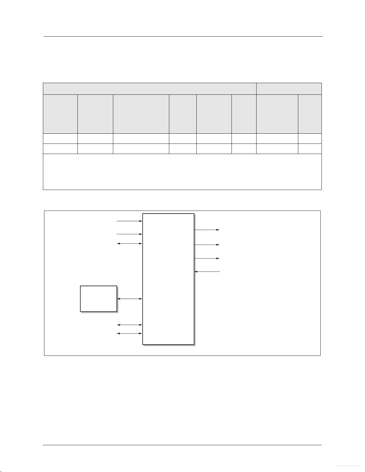
Table 1 shows the different devices and the functions that are supported for each.
Figure 1 illustrates the CX20671 devices and major signal interfaces.
Table 1. CX20671 Models and Functions
Model/Order/Part Numbers Supported Functions
SmartDAA4
Line Side
Device (LSD)
[16-Pin QFN]
Part Number
V.92
Modem
Number of
DACs/ADCs
Device Set
Order
Number
Audio Codec
Part Number
Codec Revision
Audio
Codec
Package
Type
CX20671-11Z CX20671 -11Z 40-QFN None N 4/6 2
CX20671-21Z CX20671 -21Z 40-QFN None N 4/6 2
GENERAL NOTES:
1. Supported functions (Y = Supported; N = Not supported).
2. All devices are lead-free (Pb-free) and RoHS-compliant, and are compatible with leaded reflow processes.
3. Contact local Conexant Sales office for advanced software options.
Figure 1. CX20671 Devices and Major Signal Interfaces
Digital
Mic
10 Conexant DSH-202291p1
Conexant Proprietary and Confidential 7/22/10
Page 11

CX20671 Data Sheet Introduction
Free Datasheet http://www.datasheet4u.com/
1.2 CX20671 Audio Codec Features
24-bit, two pairs of independent DACs and three pairs of independent ADCs
ProCoustic headphone driver, which delivers 50 mW into 32 Ω load with no pop,
eliminating the need for an external amplifier and DC-blocking capacitors
Integrated 5 V to 3.3 V low-dropout voltage regulator for improved audio
performance, eliminating need for external regulator or power transistor
Integrated 3.3 V to 1.8 V low-dropout voltage regulator, used to power digital
blocks
Integrated 2 WRMS (per channel) class-D stereo speaker amplifier with Spread
Spectrum and 10-kV ESD withstand capability
Digital Microphone interface with internal MIC boost supporting 2 digital
microphone elements
Independent Sony Philips Digital Interface (SPDIF) Output supporting sample rates
44.1 kHz, 48 kHz, and 96 kHz, 16, 20, and 24-bit resolution
Internal microphone boost
– Digital: 0, 12, 24, 36, 48 dB
– Analog: 0, 10, 20, 30, 40 dB
Microphone Security Control (Contact Conexant Sales/FAE for additional
information).
Exceeds Vista/Windows 7 Desktop and Notebook Premium Logo Requirements,
WLP4.0
D-Flex power management exceeds Intel ECR 15B requirements, and features
Wake-On-PCBeep functionality
Hardware Headphone limiter bit (supports GS Mark EN50332-2)
Compliant with Intel High Definition Audio Specification Rev. 1.0
Supports both 1.5 V and 3.3 V signaling with the core logic chipset
Retaskable ports
– Configure between Headphone and Line-out or between Mic and Line-in
Independent sampling rate for DAC and ADC; supports audio formats ranging from
16-bit, 44.1 kHz to 24-bit, 192 kHz
Pop Shield: pops and clicks reduction circuitry, including class-D speaker outputs
Jack sense detects up to four jacks using only one sense pin
Digital Mixer
+3.3 V analog and I/O operation; uses Vaux for power management modes
Audio Director for Headphone and Internal Speakers Redirection (optional).
– Supporting Classic Mode
– Vista/Windows 7 Multi-Stream
– Custom Multi-Stream Mode
Voice Processing Algorithms (optional)
DSH-202291p1 Conexant 11
7/22/10 Conexant Proprietary and Confidential
Page 12

Introduction CX20671 Data Sheet
Free Datasheet http://www.datasheet4u.com/
– End-to-end Noise Reduction (patent pending)
– Multi-band Acoustic Echo Cancellation
– Side Noise Rejection Beam Forming
SmartAudio GUI (optional) - advanced audio control
Digital Parametric SmartEQ with Dynamic Compression DSP (optional)
– Enhances the sound quality on low cost speakers
– Night Mode
3D Expander
Third Party Logo Software support includes
–SRS
– Dolby
– Creative Labs
– ForteMedia
– Andrea
– MaaxAudio
– Virage Logic
Supports 32-bit/64-bit Windows OS and Linux
Available in 40-pad thermally-enhanced QFN package
1.3 System Compatibility
System compatibility
– Windows XP/Vista/Windows 7 operating system on a 1 GHz-based computer
with 512 MB RAM, or equivalent
– Microsoft Vista/Windows 7 Premium Logo compliant, WLP4.0
– Linux Kernel (contact local Conexant Sales Office for details)
1.4 Hardware Qualification Process
The Hardware Qualification Process (HQP) is intended to improve the quality and
reliability of ODM custom boards being shipped to PC OEMs. The goals of this
process are to:
Eliminate common design mistakes
Ensure boards perform well and pass DTM Fidelity requirements with good margin
Eliminate potential manufacturing issues that may result from a marginal design
Eliminate country specific issues
Eliminate common INF problems
Converge towards standard designs
12 Conexant DSH-202291p1
Conexant Proprietary and Confidential 7/22/10
Page 13

CX20671 Data Sheet Introduction
Free Datasheet http://www.datasheet4u.com/
The HQP includes review of schematics, board layout, and BOM (Bill of Material). All
boards must meet the pre-defined criteria. Contact the local Conexant Sales office for
more details about the HQP process.
HQP must be performed for all OEM designs.
DSH-202291p1 Conexant 13
7/22/10 Conexant Proprietary and Confidential
Page 14

Introduction CX20671 Data Sheet
Free Datasheet http://www.datasheet4u.com/
14 Conexant DSH-202291p1
Conexant Proprietary and Confidential 7/22/10
Page 15

2
Free Datasheet http://www.datasheet4u.com/
Hardware Interface
2.1 General
2.1.1 HD Audio Host Interface
The HD Audio host interface conforms to HD Audio (Rev. 1.0)
The supported HD Audio signals are as follows:
Bit Clock (BIT_CLK), input
Frame Sync (SYNC), input
Serial Data Output (SDATA_OUT), input
Serial Data Input (SDATA_IN), input/output
Master Hardware Reset (RESET#), input
2.1.2 Control Signals
Control signals supported from straps or the host are as follows:
External Amplifier Power Down (EAPD#), output
Class-D speaker mute (SPK_MUTE#), input
Jack sensing (SENSEA), input
General-purpose inputs/outputs (GPIO0, GPIO1)
2.1.3 Audio Signals
Audio interface signals supported are as follows:
Port A (PORTA_L and PORTA_R), ProCoustic headphone output/line output
Port B (PORTB_L and PORTB_R), microphone input/line input, with microphone
bias voltage
Port C (PORTC_L and PORTC_R), microphone input/line input/line output, with
microphone bias voltage
Port G (LEFT+ and RIGHT+), Class-D speaker amplifier stereo output
Digital Stereo Microphone (DIGITAL_MIC_1/2), digital microphone input, dual
array
PC Speaker Beep pass-through (PC_BEEP), input
Sony Philips Digital Interface (SPDIF) Output
DSH-202291p1 Conexant 15
7/22/10 Conexant Proprietary and Confidential
Page 16
Hardware Interface CX20671 Data Sheet
HDA
Link
Inter fac
e
Reset#
BIT_CLK
SYNC
SDI
SDO
GPIO0/EAPD#
GPIO1/SPK_MUT E
#
CLOCK
Digital
Microphon
e
1A
1B
MIC/LINE IN
MIC/LINE I/O
MIC BIAS
MIC BIAS
Port B
Port
C
DA
C
10
DAC
11
1F
Port G
19
Port A
HP
LINE OUT
CLASS_D
AM
P
PC BEEP
BEEP
13
SENSE A
DATA 1/2
23
Port
J
Boos
t
17
18
ADC
14
ADC
15
ADC
16
24
12
20
Port
H
SPDIF
DCO
Free Datasheet http://www.datasheet4u.com/
2.2 CX20671 Block Diagram
Figure 2 provides a simplified block diagram of the CX20671.
Figure 2. CX20671 Block Diagram
16 Conexant DSH-202291p1
Conexant Proprietary and Confidential 7/22/10
Page 17
CX20671 Data Sheet Hardware Interface
SPDIF
PC_BEEP
DM IC_1/2
DMIC_CLK0
LEFT -
LEFT +
RIGHT-
RIGHT+
PORT A_L
PORT A_R
NC
NC
PORT B_L
PORT B_R
PORT C_L
PORT C_R
B_BIAS
C_BIAS
SENSEA
FILT_1.65
39
10
1
40
13
11
14
16
22
23
24
25
34
35
30
31
33
32
36
29
SYNC
BIT_CLK
SDATA_ OU T
SDATA_ IN
RESET#
GPIO 0/EAPD #
GPIO 1/SPK _MU T E#
FLY_P
FLY_N
AVEE
AVDD _HP
VDD _IO
VAUX _3.3
DVDD_3.3
FILT_1.8
AVDD _5V
AVDD _3.3
RPW R_5.0
LPW R_5 .0
CLASS-D_REF
GND
8
5
4
6
9
38
37
19
20
21
26
7
2
18
3
28
27
15
12
17
4
1
Charge Pum p Flying C ap
Class-D Am
p
Reference Voltag
e
Mic Bias
Jack Sens
e
HD A Bus
Signal
s
HD A Bus Signaling Voltage
Standby Supply Voltage
+3.3V S upply Voltage for Digital
+1.8V Core R egulator Bypas
s
GPIO
s
-2.0 V or -2.6 V C h arg e Pu m p B y pas s
+3.3V Headphone Pow e
r
Pin 4 1 refers to
exposed
ground paddl
e
5V -to-3.3V Regulator Input
5V-to-3.3V Regulator Outpu
t
Class-D Am p Right C h. Supply
Class-D Am p Left C h. Supply
Class-D Ref. Voltag
e
Audio Signal
s
PC_Beep
DM IC Interfac
e
NC
NC
CX20671
40-Pin QFN
S/PDIF Out
Free Datasheet http://www.datasheet4u.com/
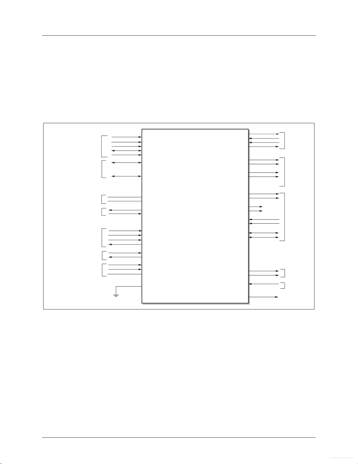
2.3 CX20671 Pin Assignments, Signal Definitions, and Electrical Characteristics
The CX20671 40-QFN device signals are shown by major interface in Figure 3, by pin
number in Figure 4, and are listed by pin number in Table 2.
Hardware interface signals are defined in Table 3.
Figure 3. CX20671 40-QFN Hardware Interface Signals
DSH-202291p1 Conexant 17
7/22/10 Conexant Proprietary and Confidential
Page 18
Hardware Interface CX20671 Data Sheet
1
2
3
4
5
6
7
8
9
1
0
1
1
1
2
1
3
1
4
1
5
1
6
1
7
1
8
1
9
2
0
4
0
3
9
3
8
3
7
3
6
3
5
3
4
3
3
3
2
3
1
D
M
IC
1
/2
V
A
U
X
_
3
.3
F
I
L
T
_
1
.8
S
D
A
T
A
_
O
U
T
B
I
T
_
C
L
K
S
D
A
T
A
_
I
N
V
D
D
_
IO
S
Y
N
C
R
E
S
E
T
#
P
C
_
B
E
E
P
P
O
R
T
C
_
L
F
I
L
T
_
1
.6
5
A
V
D
D
_
5
V
A
V
D
D
_
3
.
3
A
V
D
D
_
H
P
N
C
N
C
P
O
R
T
A
_
R
P
O
R
T
A
_
L
A
V
E
E
D
M
I
C
_
C
L
K
G
P
IO
0
/
E
A
P
D
#
G
P
IO
1
/
S
P
K
_
M
U
T
E
#
S
E
N
S
E
_
A
P
O
R
T
B
_
R
P
O
R
T
B
_
L
B
_
B
IA
S
C
_
B
I
A
S
P
O
R
T
C
_
R
L
E
F
T
+
L
P
W
R
_
5
.0
L
E
F
T
-
R
IG
H
T
-
R
P
W
R
_
5
.0
R
IG
H
T
+
C
L
A
S
S
-
D
_
R
E
F
D
V
D
D
_
3
.3
F
L
Y
_
P
F
L
Y
_
N
3
0
2
9
2
8
27
2
6
2
5
2
4
2
3
2
2
2
1
CX20671
SPDIF
CONEXANT
TM
Free Datasheet http://www.datasheet4u.com/
Pin Define
Please help add Pin41 GND for Thermal Pad
Figure 4. CX20671 40-QFN Pad Signals
18 Conexant DSH-202291p1
Conexant Proprietary and Confidential 7/22/10
Page 19

CX20671 Data Sheet Hardware Interface
Free Datasheet http://www.datasheet4u.com/
Table 2. CX20671 Pad Signals
Pad Number Signal Name Pad Number Signal Name
1 DMIC_1/2 21 AVEE
2 VAUX_3.3 22 PORTA_L
3 FILT_1.8 23 PORTA_R
4 SDATA_OUT 24 NC
5 BIT_CLK 25 NC
6 SDATA_IN 26 AVDD_HP
7 VDD_IO 27 AVDD_3.3
8 SYNC 28 AVDD_5V
9 RESET# 29 FILT_1.65
10 PC_BEEP 30 PORTC_L
11 LEFT+ 31 PORTC_R
12 LPWR_5.0 32 C_BIAS
13 LEFT- 33 B_BIAS
14 RIGHT- 34 PORTB_L
15 RPWR_5.0 35 PORTB_R
16 RIGHT+ 36 SENSE_A
17 CLASS-D_REF 37 GPIO1/SPK_MUTE#
18 DVDD_3.3 38 GPIO0/EAPD#
19 FLY_P 39 SPDIF
20 FLY_N 40 DMIC_CLK
(1)
41
FOOTNOTES:
(1)
Pad 41 refers to the exposed pad at the bottom of the device. This thermal/electrical pad must be connected to PCB ground plane with
GND (Note 1)
enough vias. It is recommended that a 4x4 grid of such vias be used.
DSH-202291p1 Conexant 19
7/22/10 Conexant Proprietary and Confidential
Page 20
Hardware Interface CX20671 Data Sheet
Free Datasheet http://www.datasheet4u.com/
Table 3. CX20671 Pad Signal Definitions (1 of 4)
Label Pad Number Type
I/O
Type
Signal Name/Description
Power
DVDD_3.3 18 PWR PWR Digital Supply Voltage. +3.3 V. Connect to system
+3.3 V.
VAUX_3.3 2 PWR PWR Standby Supply Voltage. +3.3 V. Connect to system's
+3.3 V Standby supply. This power pin is used to
support Wake-on-Jack functions.
VDD_IO 7 PWR PWR Input/Output Signaling Voltage Supply. Determines
the signaling voltage that is being used on the host
system. When VDD_IO is +1.5 V, the device will use
1.5 V signaling on the HDA interface pins; when
VDD_IO is +3.3 V, the device will use 3.3 V signaling
on the HDA interface pins.
FILT_1.8 3 PWR PWR Internally Regulated Digital Core Supply Voltage.
+1.8 V + 5%. Connect to external decoupling
capacitor.
AVD D_5 V 28 P WR P WR Analog Supply Input Voltage for LDO. +5.0 V.
Connect to system +5.0 V supply.
AVD D_3 .3 2 7 P WR PW R Output Voltage from LDO. +3.3 V +
5%. Connect to
external decoupling capacitor.
AVD D_H P 26 P WR PWR Supply Input Voltage for Headphone Amplifiers.
+3.3 V. Connect to system +3.3 V.
RPWR_5.0 15 PWR PWR Supply Voltage for Class-D Amplifier, Right
Channel. +5.0 V. Connect to LPWR_5.0.
Connect LPWR_5.0/RPWR_5.0 to system +5.0 V
supply through a 0.1 Ω resistor.
LPWR_5.0 12 PWR PWR Supply Voltage for Class-D Amplifier, Left Channel.
+5.0 V. Connect to RPWR_5.0.
Connect LPWR_5.0/RPWR_5.0 to system +5.0 V
supply through a 0.1 Ω resistor.
FLY_N 20 PWR PWR Charge Pump Negative Transfer Charge.
Connected to FLY_P through a 2.2 μF or 1.0 μF
capacitor.
FLY_P 19 PWR PWR Charge Pump Positive Transfer Charge. Connected
to FLY_N through a 2.2 μF or 1.0 μF capacitor.
AVEE 21 PWR PWR Internally Generated Analog Negative Supply.
Connect to external decoupling capacitor.
-2.6 V when HP output set at 1.2 Vrms + 10%
-2.0 V when HP output set at 1.0 Vrms +
10%
20 Conexant DSH-202291p1
Conexant Proprietary and Confidential 7/22/10
Page 21
CX20671 Data Sheet Hardware Interface
Free Datasheet http://www.datasheet4u.com/
Table 3. CX20671 Pad Signal Definitions (2 of 4)
Label Pad Number Type
I/O
Type
Signal Name/Description
Ground
GND 41 GND GND Audio Device Ground. This is thermal/electrical GND
paddle of device. Connect to audio ground.
High Definition Audio Interface
BIT_CLK 5 I Ihd Bit Clock. 24 MHz serial data input bit clock from the
HDA link.
Connect to BITCLK.
SYNC 8 I Ihd Frame Sync. 48 kHz fixed rate sample HDA sync
input. Synchronization pulse from an HDA compliant
controller to all of the HDA compliant codecs on the
link. This signal is nominally 0.167 μs wide pulse that
is used to synchronize the HDA. Reset state = low.
Standard load = 50 pF. SYNC is derived from dividing
BITCLK by 500.
Connect to SYNC.
SDATA_OUT 4 I Ihd
Serial Data Output. Serial input data stream from
an HDA controller. Reset state = low. Standard
load = 50 pF
.
Connect to SDATA_OUT through 33 Ω
SDATA_IN 6 I/O Ohd Serial Data Input. Serial output data stream to the
HDA controller. Functions as an input during codec
initialization. Controller has a weak pull-down resistor
to prevent spurious events in electrically noisy
environments.
Connect to SDATA_IN through 33 Ω
RESET# 9 I Ihdl Master Hardware Reset. Active low HDA link reset
signal. The minimum width of this pulse must be 100
μs.
Connect directly to RESET.
Reference Voltage Connections
FILT_1.65 29 REF REF Analog Reference Voltage. 1.65 V + 5%. Connect to
external decoupling capacitor.
CLASS-D_REF 17 REF REF Class-D Amplifier Reference Voltage. Connect to
RPWR_5.0/LPWR_5.0 voltage supply through
external capacitor.
DSH-202291p1 Conexant 21
7/22/10 Conexant Proprietary and Confidential
Page 22

Hardware Interface CX20671 Data Sheet
Free Datasheet http://www.datasheet4u.com/
Table 3. CX20671 Pad Signal Definitions (3 of 4)
Label Pad Number Type
I/O
Type
Signal Name/Description
General Purpose Input/Outputs
GPIO0/EAPD# 38 I/O It/Ot External Amplifier Power-Down Signal/ General
Purpose I/O. EAPD# is an active-low output.
If EAPD = 0, power down the external amplifier.
If EAPD = 1, power up the external amplifier
GPIO1/SPK_MUTE# 37 I/O It/Ot General Purpose I/O, Class-D Speaker Amplifier Mute
Input. SPK_MUTE# is a active-low input.
Audio Digital Signals
PC_BEEP 10 I Id PC Speaker Beep Pass-Through. Input. Logic-level
BEEP signal needs to be ac-coupled to this pin.
DMIC_1/2 1 I Id Stereo Digital Microphone Data. Input
DMIC_CLK 40 O Od Digital Microphone Clock. Output
SPDIF 39 O It/Ot Sony Philips Digital Interface (SPDIF) output.
Note: For -21Z devices only, a pull-down on this pin
sets PC BEEP gain to -18 dB while the codec is in
RESET.
Audio Analog Signals
These signals connect to analog sources and sinks, including microphones and speakers.
PORTB_L 34 I Ia Microphone Input/Line Input, Left Channel. With
microphone bias voltage.
PORTB_R 35 I Ia Microphone Input/Line Input, Right Channel. With
microphone bias voltage.
B_BIAS 33 REF REF Microphone Bias Voltage for Port B.
PORTC_L 30 I Ia, Oa Microphone Input/Line Input/Line Output, Left
Channel. With microphone bias voltage.
PORTC_R 31 I Ia, Oa Microphone Input/Line Input/Line Output, Right
Channel. With microphone bias voltage.
C_BIAS 32 REF REF Microphone Bias Voltage for Port C.
LEFT+ 11 O Oa Class-D Amplifier Output, Left Channel, Positive.
LEFT- 13 O Oa Class-D Amplifier Output, Left Channel, Negative.
RIGHT+ 16 O Oa Class-D Amplifier Output, Right Channel, Positive.
RIGHT- 14 O Oa Class-D Amplifier Output, Right Channel, Negative.
PORTA_L 22 O Oa Headphone Output/Line Output, Left Channel. This
is a ProCoustic (cap-less) headphone output.
PORTA_R 23 O Oa Headphone Output/Line Output, Right Channel.
This is a ProCoustic (cap-less) headphone output.
22 Conexant DSH-202291p1
Conexant Proprietary and Confidential 7/22/10
Page 23

CX20671 Data Sheet Hardware Interface
Free Datasheet http://www.datasheet4u.com/
Table 3. CX20671 Pad Signal Definitions (4 of 4)
Label Pad Number Type
I/O
Type
Signal Name/Description
SENSE_A 36 I Ia SENSE A Input.
Reserved/Not Used
NC 25 - - Not Used. Leave unconnected.
NC 24 - - Not Used. Leave unconnected.
NC 39 - - Not Used. Leave unconnected.
GENERAL NOTES:
I/O types:
Ia Analog input
Oa Analog output
Od Digital output
Ohd Digital output, HD Audio-compatible
Id Digital input, with pull-down
Ihd Digital input, HD Audio-compatible
It Digital input, TTL-compatible
Table 4 lists the device's absolute maximum ratings.
Table 5 lists the electrical characteristics for the Digital Mic interface.
Table 6 lists the devices' DC characteristics for the TTL-compatible I/Os.
Table 7 lists the host's required DC characteristics for the HD Audio interface signals.
Table 4. Absolute Maximum Ratings
Parameter Symbol Limits Units
Supply Voltage DVDD_3.3 3.6 V
VAUX_3.3 3.6
VDD_IO 3.6/1.65
(1)
AVDD_HP 3.6
AVDD_5V 5.5
RPWR_5.0 5.5
LPWR_5.0 5.5
Digital Input Voltage V
Analog Input Voltage V
DC Clamp Current, Input I
DC Clamp Current, Output I
Storage Temperature Range T
FOOTNOTES:
(1)
Depends on 3.3 volts or 1.5 volts HD Audio signaling level.
ind
ina
ik
ok
stg
-0.7 to 4.0 V
-0.7 to 4.0 V
+ 20 mA
+ 20 mA
-55 to 125 °C
DSH-202291p1 Conexant 23
7/22/10 Conexant Proprietary and Confidential
Page 24

Hardware Interface CX20671 Data Sheet
Free Datasheet http://www.datasheet4u.com/
Table 5. DC Characteristics –Digital Microphone
Parameter Symbol Minimum Typical Maximum Units Notes
Input Voltage Low V
Input Voltage High V
Output Voltage Low V
Output Voltage High V
IL
IH
OL
OH
–0.3 — 0.94 V Max. value adjustable
1.2 — 3.3 V
——0.4V
2.6 — — V
Drive Strength 0.3 4 6.8 mA Adjustable
GENERAL NOTES: Test Conditions unless otherwise stated: DVDD = +3.3 ± 0.165 VDC; TA = 0°C to 70°C.
Table 6. DC Characteristics – TTL Compatible (EAPD#, GPIOs)
Parameter Symbol Minimum Typical Maximum Units Notes
Input Voltage V
Input Voltage Low V
Input Voltage High V
Output Voltage Low V
Output Voltage High V
GPIO Output sink current at 0.4 V
IN
IL
IH
OL
OH
———12mA
——4.0V
–0.5 — 0.8 V
2.0 — Vdd+0.5 V
0—0.4V
2.4 — Vdd V
maximum
GPIO Output source current at 2.97 V
———12mA
minimum
GPIO rise/fall time — — — 4 ns 25% to 75%
GENERAL NOTES: Test Conditions unless otherwise stated: DVDD = +3.3 ± 0.165 VDC; TA = 0°C to 70°C; external load = 50 pF
24 Conexant DSH-202291p1
Conexant Proprietary and Confidential 7/22/10
Page 25

CX20671 Data Sheet Hardware Interface
Free Datasheet http://www.datasheet4u.com/
Table 7. Host Signal Characteristics – HD Audio
Parameter Symbol Minimum Maximum Units Test Conditions
HD Audio Signal Levels at 3.3 V
VDD_IO V
Input High Voltage V
Input Low Voltage V
Output High Voltage V
Output Low Voltage V
Output High Voltage - AC Drive Point V
Output Low Voltage - AC Drive Point V
Input leakage Current I
VDD_IO V
Input High Voltage V
Input Low Voltage V
Output High Voltage V
Output Low Voltage V
CC
IH
IL
OH
OL
OHAC
OLAC
IL
3.135 3.465 V VCC < VDD + 0.5 V
0.65 x V
CC
0.35 x V
0.9 x V
CC
0.10 x V
0.7 x V
CC
0.3 x V
±10 µA 0 < VIN < V
HD Audio Signal Levels at 1.5 V
CC
IH
IL
OH
OL
1.35 1.65 V VCC < VDD + 0.5 V
0.6 x V
CC
0.4 x V
0.9 x V
CC
0.10 x V
V
CC
VI
CC
VI
CC
V
= 500 µA
OUT
VI
VI
= 1500 µA
OUT
= -15 x VCC mA
OUT
= 15 x VCC mA
OUT
CC
V
CC
VI
CC
V
= 500 µA
OUT
VI
= 1500 µA
OUT
Output High Voltage - AC Drive Point V
Output Low Voltage - AC Drive Point V
Input leakage Current I
OHAC
OLAC
IL
0.7 x V
CC
0.3 x V
VI
CC
±10 µA 0 < VIN < V
GENERAL NOTES:
1. The supply voltage refers to the VDD_IO pin.
2. Test Conditions unless otherwise stated: DVDD = +3.135V to +3.465 V; TA = 0 °C to 70 °C.
= -9.38 x VCC mA
OUT
VI
= 9.38 x VCC mA
OUT
CC
DSH-202291p1 Conexant 25
7/22/10 Conexant Proprietary and Confidential
Page 26

Hardware Interface CX20671 Data Sheet
Free Datasheet http://www.datasheet4u.com/
Figure 5. Output Butter for 3.3 V Signaling
Figure 6. CX20671 Output Buffer for 1.5 V Signaling
26 Conexant DSH-202291p1
Conexant Proprietary and Confidential 7/22/10
Page 27

CX20671 Data Sheet Hardware Interface
Free Datasheet http://www.datasheet4u.com/
2.4 Device Performance Specifications
The following tables and graphs illustrate the device’s analog performance.
Table 8. CX20671 Analog Performance Characteristics (1 of 2)
Parameter Minimum Typical Maximum Units
Line Outputs
Full Scale Output Voltage 1.0 Vrms
Dynamic Range (measured with -60 dBFS signal present) 97 dBFS
Total Harmonic Distortion + Noise (THD + N), measured at -3 dBFS -90 -93 dB
Channel Crosstalk -84 dBFS
Analog Frequency Response (+/- 3 dB at 20 Hz, +/- 1 dB at 20000 Hz) 20 20000 Hz
Headphone Output
Full Scale Output Voltage 1.2 Vrms
Dynamic Range (measured with -60 dBFS signal present) 97 dBFS
Total Harmonic Distortion + Noise (THD + N), measured at -3 dBFS -85 dB
Channel Crosstalk -75 dBFS
Analog Frequency Response (+/- 3 dB at 20 Hz, +/- 1 dB at 20000 Hz) 20 20000 Hz
Class-D Speaker Amplifier Outputs
Full Scale Output Voltage (into 4 Ω) 3.96
2.83
Dynamic Range (measured with -60 dBFS signal present) 92 dBFS
Total Harmonic Distortion + Noise (THD + N, measured at -3 dBFS) -70 dBFS
Analog Frequency Response (+/- 3 dB at 20 Hz, +/- 1 dB at 20000 Hz) 20 20000 Hz
Efficiency (Measured at 1 W/Ch) 85 %
4.0
2.90
4.2
3
Vp
Vrms
Line Inputs
Full Scale Input Voltage 1.0 Vrms
Dynamic Range (measured with -60 dBFS signal present) 89 dBFS
Total Harmonic Distortion + Noise (THD + N), measured at -3 dBFS -87 dB
Channel Crosstalk -84 dBFS
Analog Frequency Response (+/- 3 dB at 200 Hz, +/- 1 dB at 20000 Hz) 200 20000 Hz
DSH-202291p1 Conexant 27
7/22/10 Conexant Proprietary and Confidential
Page 28

Hardware Interface CX20671 Data Sheet
Free Datasheet http://www.datasheet4u.com/
Table 8. CX20671 Analog Performance Characteristics (2 of 2)
Parameter Minimum Typical Maximum Units
Line Inputs (continued)
Input Resistance
0 dB
10-40 dB
15.8
5.0
kΩ
Input Capacitance 5 pF
Microphone Inputs
Full Scale Input Voltage (With 20 dB boost)
Full Scale Input Voltage (With boost off)
0.1
1.0
Vrms
Dynamic Range (measured with -60 dBFS signal present) 89 dBFS
Total Harmonic Distortion + Noise (THD + N), measured at - 3 dBFS -83.4 dBFS
Channel Crosstalk (measured at 1 kHz, 0 dB gain) -84 dBFS
Analog Frequency Response (+/- 3 dB at 200 Hz, +/- 1 dB at 20000 Hz) 200 20000 Hz
Input Resistance
0 dB
10-40 dB
15.8
5.0
kΩ
Input Capacitance 5 pF
28 Conexant DSH-202291p1
Conexant Proprietary and Confidential 7/22/10
Page 29

CX20671 Data Sheet Hardware Interface
Free Datasheet http://www.datasheet4u.com/
Figure 7. Class-D Speaker Amplifier Magnitude Frequency Response (16 bit, 48 kHz)
DSH-202291p1 Conexant 29
7/22/10 Conexant Proprietary and Confidential
Page 30

Hardware Interface CX20671 Data Sheet
THD+N vs Frequency
-90.0
-80.0
-70.0
-60.0
-50.0
-40.0
-30.0
-20.0
-10.0
0.0
100 1000 10000 1000 00
Freq (Hz)
THD+N (dBFS)
Class-D Amplifier Supply Rejection
30.0
35.0
40.0
45.0
50.0
55.0
60.0
65.0
70.0
100.0E+0 1.0E+3 10.0E+3 100.0E+3
Frequency (Hz)
Rejec tio n (dB)
5 V Supply
Free Datasheet http://www.datasheet4u.com/
Figure 8. CX20671 THD+N versus Frequency, for Class-D Amplifier Output
Figure 9. CX20671 Power Supply Rejection, for Class-D Amplifier Output
30 Conexant DSH-202291p1
Conexant Proprietary and Confidential 7/22/10
Page 31

CX20671 Data Sheet Hardware Interface
Headphone Amplifier Supply Rejection
30.0
40.0
50.0
60.0
70.0
80.0
90.0
100.0E+0 1.0E+3 10.0E+3 100.0E+3
Frequency (Hz)
Rejec tio n (dB)
3.3 V Su pp ly
Class-D Output Power vs. Load
(1% THD)
0
0.2
0.4
0.6
0.8
1
1.2
1.4
1.6
1.8
2
456789101112
Loa d (Ohm s)
Output Po wer (W)
Free Datasheet http://www.datasheet4u.com/
Figure 10. CX20671 Power Supply Rejection, for Headphone Amplifier Output
Figure 11. CX20671 Class-D Output Power vs. Load (1% THD)
DSH-202291p1 Conexant 31
7/22/10 Conexant Proprietary and Confidential
Page 32

Hardware Interface CX20671 Data Sheet
Free Datasheet http://www.datasheet4u.com/
2.5 Power Management and Power Consumption
2.5.1 Power Management
Advanced power management features allow the device to conserve additional power
by disabling/enabling individual functional blocks. This is shown in Table 9.
Table 9. Power Management
Functional Block D0 (S0-Idle)
D2 (S0-Idle)
Pre-ECR 15B
D3 (S0-Idle)
EPSS ECR
15B
D-Flex
(1)
D3 (S3)
or
D4 (S3)
D3 (S4)
(2)
or
D4 (S4)
DAC On Off Off Flex mode Off Off
ADC On Off Off Flex mode Off Off
Ports On Off Off Flex mode Off Off
Headphone Amps On Off Off Flex mode Off Off
5V LDO OnOnOnOnOff
3
Off
3
Class-D Amp On Off Off Flex mode Off Off
Reference Voltage (1.65 V) On On On On Off Off
Port Sense OnOnOnOnOffOff
HD-Audio Bus OnOnOnOnOffOff
Reg Banks OnOnOnOnOnOff
AVDD_HP Supply On On On On Off
DVDD_3.3 Supply On On On On Off
(3)
(3)
Off
Off
(3)
VDD_IO Supply On On On On On Off
VAUX_3.3 Supply On On On On On Off
FOOTNOTES:
(1)
D-Flex mode requires loading Conexant proprietary driver. D-Flex will conserve additional power by disabling/enabling certain digital and
analog blocks in the codec based on the audio activity.
(2)
In EPSS ECR-15B, the device will be set to D4 when the system goes to S3 or S4.
(3)
The supplies may remain on or off depending on the system.
32 Conexant DSH-202291p1
Conexant Proprietary and Confidential 7/22/10
Page 33

CX20671 Data Sheet Hardware Interface
Free Datasheet http://www.datasheet4u.com/
Table 10. Device Power State Mapping
Device State
(Pre-ECR 15B)
Device State
(EPSS ECR 15B)
System State Wake-up Time Description
D0 D0 S0 -- Device is in Full Power
D1 D1, D2 S0-Idle 1 ms Lower power standby (LP1). Transition time to full
10 ms Lowest power standby (LP2). Transition time to full
D2 D3 S0-Idle
75 ms
D3 D4 S3 200 ms Standby, prepare for shutdown (SD). Transition
D3 D4 S4 200 ms Hibernate, prepare for shutdown (SD). Transition
2.5.2 Power Supply Current Consumption
Table 11 shows the required voltages at the various supply input pins of the devices.
Table 11. CX20671 DC Supply Voltages
power is 1 ms.
power is 10 ms, and additional 75 ms for Full
Fidelity.
time to full power 200 ms.
time to full power 200 ms.
Parameter Symbol Minimum Typical Maximum Units Notes
Digital Voltage Supply DVDD_3.3 3.165 3.3 3.465 V
Standby Voltage Supply VAUX_3.3 3.165 3.3 3.465 V
HDA Bus Signaling Supply, 3.3V VDD_IO 3.165 3.3 3.465 V
HDA Bus Signaling Supply, 1.5 V VDD_IO 1.425 1.5 1.575 V
Class-D Amp Supply, Left Ch. LPWR_5.0 4.75 5.0 5.25 V
Class-D Amp Supply, Left Ch RPWR_5.0 4.75 5.0 5.25 V
Headphone Voltage Supply AVDD_HP 3.165 3.3 3.465 V
5V-to-3.3V Regulator Input AVDD_5V 4.75 5.0 5.25 V
Additionally, the following power-sequencing requirements must be met:
For best performance of audible pop/click suppression, VAUX_3.3 supply should
always ramp up before any of the other power supplies, and should ramp down
after all other power supplies have ramped down. It is highly recommended that
VAUX_3.3 voltage be near its final value before beginning ramp-up of AVDD_5V
rail.
DVDD_3.3 should always be present when AVDD_5V is present. If DVDD_3.3 is
removed when AVDD_5V is present, the device may be damaged.
DSH-202291p1 Conexant 33
7/22/10 Conexant Proprietary and Confidential
Page 34

Hardware Interface CX20671 Data Sheet
Free Datasheet http://www.datasheet4u.com/
All 5 V supplies (AVDD_5V, LPWR_5.0, RPWR_5.0) can be removed while
DVDD_3.3 is present.
To support Wake-On-Jack functionality, VAUX_3.3 and VDD_IO should be
powered from a power supply that is never removed (unless AC power is
removed). If no such support is required, VAUX_3.3 and VDD_IO can be powered
from same supply as DVDD_3.3. Sense resistors should ALWAYS use same
supply as VAUX_3.3 power pin.
The current and power consumption for each of the power pins is shown in Tables 12
through 15.
Table 12. D0 (S0) Full-Duplex Power Consumption
D0 (S0-Full Duplex)
(1)
Pre ECR-15B
Class Driver
Pre ECR-15B
CNXT Driver
EPSS (ECR-15B)
Class Driver
5V Class-D (mA) 1007.3 1008.01 1007.3
5V LDO (mA) 12.7 21.99 12.7
AVDD_HP (mA) 0.4 0.5 0.4
DVDD_3.3 (mA) 0.8 0.7 0.8
VDD_IO (mA) 0.031 0.061 0.031
VAUX_3.3 (mA) 48.7 46.2 48.7
Class-D Power (mW) 5036.50 5040.05 5036.50
LDO Power (mW) 21.59 37.38 21.59
Rest of the chip (mW) 206.68 229.19 206.68
Total Power (mW) 5264.77 5306.62 5264.77
FOOTNOTES:
(1)
Transmitting full-scale sinewave from Class-D, recording using analog microphone.
34 Conexant DSH-202291p1
Conexant Proprietary and Confidential 7/22/10
Page 35

CX20671 Data Sheet Hardware Interface
Free Datasheet http://www.datasheet4u.com/
Table 13. Pre-ECR15B D-States Power Consumption With Class Driver
Pre ECR-15B D-States (Class Driver)
D0 (S0-Idle) D3 (S3)
(1)
D3 (S4)
5V Class-D (mA) 7.6 0.6 0
5V LDO (mA) 18.28 0.95 0
AVDD_HP (mA) 0.5 0.4 0
DVDD_3.3 (mA) 0.7 0.1 0
VDD_IO (mA) 0.035 0.007 0.000
VAUX_3.3 (mA) 46.9 2.2 0
Class-D Power (mW) 38.00 3.00 0.00
LDO Power (mW) 31.08 1.62 0.00
Rest of the chip (mW) 219.17 12.07 0.00
Total Power (mW) 288.25 16.68 0.00
FOOTNOTES:
(1)
In Suspend mode (S3 or S4), the device state will be D3.
Table 14. Pre-ECR15B D-States Power Consumption With Conexant Driver
(1)
Pre ECR-15B D-States (Conexant Driver)
D2 (S0-Idle) D3 (S3)
(1)
D3 (S4)
5V Class-D (mA) 0.6 0.5 0
5V LDO (mA) 1.02 0.99 0
AVDD_HP (mA) 0.4 0.4 0
DVDD_3.3 (mA) 0.1 0.1 0
VDD_IO (mA) 0.036 0.007 0.000
VAUX_3.3 (mA) 6.8 2.1 0
Class-D Power (mW) 3.00 2.50 0.00
LDO Power (mW) 1.73 1.68 0.00
Rest of the chip (mW) 27.57 11.87 0.00
Total Power (mW) 32.31 16.05 0.00
FOOTNOTES:
(1)
In Suspend mode (S3 or S4), the device state will be D3.
(1)
DSH-202291p1 Conexant 35
7/22/10 Conexant Proprietary and Confidential
Page 36

Hardware Interface CX20671 Data Sheet
Free Datasheet http://www.datasheet4u.com/
Table 15. EPSS ECR15B D-States Power Consumption with Conexant Driver
EPSS ECR-15B D-States (Conexant Driver)
D3 (S0-Idle)
(1)
D4 (S3)
(2)
D4 (S4)
5V Class-D (mA) 0.6 0.5 0
5V LDO (mA) 1.02 0.99 0
AVDD_HP (mA) 0.4 0.4 0
DVDD_3.3 (mA) 0.1 0.1 0
VDD_IO (mA) 0.134 0.007 0.000
VAUX_3.3 (mA) 2 2.1 0
Class-D Power (mW) 3.00 2.50 0.00
LDO Power (mW) 1.73 1.68 0.00
Rest of the chip (mW) 12.06 11.87 0.00
Total Power (mW) 16.79 16.05 0.00
FOOTNOTES:
(1)
In S0-Idle mode, the device will be set to D3; BCLK is removed.
(2)
In Suspend mode (S3 or S4), the device state will be D4. In S4 mode, power supplies are removed.
(2)
2.5.3 Integrated Low-Dropout Regulators
The devices feature two integrated low-dropout voltage regulators:
A 5 V to 3.3 V regulator: The output of this voltage regulator (AVDD_3.3) can be
used to power external circuitry (low-power analog for example). However, external
current consumption from the regulator should be limited to no more than 30 mA.
Additionally, caution should be used when powering external circuitry; use filtering
(ferrite bead + capacitor, for example) to prevent the external circuitry from adding
noise to the AVDD_3.3 voltage rail.
A 3.3 V to 1.8 V regulator: The output of this voltage regulator (FILT_1.8) can also
be used to power external circuitry (discrete logic, for example).
36 Conexant DSH-202291p1
Conexant Proprietary and Confidential 7/22/10
Page 37

CX20671 Data Sheet Hardware Interface
Free Datasheet http://www.datasheet4u.com/
2.6 Integrated High-Pass Filter
The CX20671 device features a hardware digital high-pass filter, intended to be used
with the class-D speaker amplifier. The cut-off frequency can be adjusted from 15 Hz
to 945 Hz, in 15-Hz steps (30 Hz to1890 Hz, in 30-Hz steps for -21Z devices),
depending on the value present in the appropriate 6-bit control register. Note that a
setting of 000000b in the control register bypasses the filter.
By default, the high-pass filter is automatically applied to the DAC that is connected
(mapped) to the class-D speaker amplifier. This “DAC tracking” mode can be disabled,
and the high-pass filter can be applied to any DAC, regardless of the port connected to
it. There are two ways to set the high-pass cut-off frequency:
DAC tracking mode: This is the typical mode of operation. This mode needs to be
enabled, as it is not the default mode. The high-pass filter tracks the DAC that is
connected to (mapped to) the class-D amplifier, but the 3 dB frequency is manually
set by writing to the 6-bit control register.
Fully manual mode: This mode needs to be enabled as it is not the default mode.
The cut-off frequency can be set manually writing to the 6-bit control register. The
DAC to which the filter is applied can also be selected manually by writing to the
appropriate control register. Note that no typical application will use this mode.
The high-pass filter response for a specific setting is shown in the figure below. Note
that, since it is a first-order filter, it rolls off at -20 dB/decade, or -6 dB/octave.
DSH-202291p1 Conexant 37
7/22/10 Conexant Proprietary and Confidential
Page 38

Hardware Interface CX20671 Data Sheet
High-Pass Frequency Response
-36
-33
-30
-27
-24
-21
-18
-15
-12
-9
-6
-3
0
1 10 100 1000 10000 100000
Frequency (H z)
Amplitude (dB)
180 Hz High-pas s Response
Free Datasheet http://www.datasheet4u.com/
Figure 12. High-Pass Filter Response
The location of registers used to control the high-pass filter cut-off frequency is in
Node ID 25h (-11Z devices) and Node ID 27h (-21Z devices)—the Vendor Widget. For
additional details, contact Conexant for the application note.
38 Conexant DSH-202291p1
Conexant Proprietary and Confidential 7/22/10
Page 39

CX20671 Data Sheet Hardware Interface
T
TT
su h
DMIC_CLK
DMIC_DATA
Dmic_clk_period
Right Mic Data Left Mic Data Right Mic Data Left Mic Data
Free Datasheet http://www.datasheet4u.com/
2.7 AC Timing Characteristics
2.7.1 Digital Microphone
The Conexant digital microphone interface on the CX20671 consists of a clock and
data pin. The digital mic clock pin provides a 3.072 MHz clock to the digital mic. The
digital mic data pin is an input, accepting multiplexed Pulse Density Modulation (PDM)
data from the digital mic. Timing waveforms are illustrated in Figure 13, and timing
parameters are listed in Table 16.
Contact Conexant Sales FAE for a list of qualified digital microphones.
Figure 13. Digital Mic Clock Timing Waveform
Table 16. Digital Mic Timing Parameters
Parameter Symbol Minimum Typical Maximum Units
DMIC_CLK frequently
DMIC_CLK period T
(1)
Dmic_clk_period
3.0689 3.072 3.0751 MHz
325.19 325.52 325.85 ns
—— 4 ns
DMIC_CLK transition period @ 50 pF
DMIC_CLK transition period @ 20 pF
DMIC_CLK transition period @ 7 pF
DMIC_DATA setup time T
DMIC_DATA hold time T
FOOTNOTES:
(1)
Worst case duty cycle restricted to 40/60.
(2)
Measured between 25% and 75% full scale.
DSH-202291p1 Conexant 39
7/22/10 Conexant Proprietary and Confidential
(2)
(2)
(2)
su
h
——1.9ns
—— 1 ns
—36—ns
0——ns
Page 40

Hardware Interface CX20671 Data Sheet
T
T
T
T
T
clk_period
sync_period
clk_low
clk_high
sync_high
BIT_CLK
SYNC
Free Datasheet http://www.datasheet4u.com/
2.7.2 HD Audio Clocks
The BIT_CLK signal is a 24 MHz clock sourced from the HD Audio controller and
connecting to all codecs on the link.
HD Audio clock waveforms and timing parameters are shown in Figure 14 and
Table 17.
Figure 14. BIT_CLK and SYNC Timing Waveforms
Table 17. BIT_CLK and SYNC Timing Parameters
Parameter Symbol Minimum Typical Maximum Units
BIT_CLK frequency 23.9976 24.0 24.0024 MHz
BIT_CLK period T
BIT_CLK output jitter — 150 500 Ps
BIT_CLK high pulse width
BIT_CLK low pulse width
SYNC frequency
SYNC period T
SYNC high pulse width T
FOOTNOTES:
(1)
47.5–70 pF external load.
(2)
Worst case duty cycle restricted to 40/60.
(3)
The SYNC frequency is equal to the BIT_CLK frequency divided by 500.
(3)
(1) (2)
(1) (2)
clk_period
T
clk_high
T
clk_low
sync_period
sync_high
41.363 41.67 41.971 ns
18.75 — 22.91 ns
18.75 — 22.91 ns
—48—kHz
—20.8—μs
—4 x T
clk_period
— μs
40 Conexant DSH-202291p1
Conexant Proprietary and Confidential 7/22/10
Page 41

CX20671 Data Sheet Hardware Interface
T
hold
T
hold
T
setup
T
co
BIT_CLK
SDATA_OUT
SDATA_IN
Free Datasheet http://www.datasheet4u.com/
2.7.3 Data Output and Input
Data output and input waveforms are illustrated in Figure 15. Timing parameters are
listed in Tables 18 and 19.
Figure 15. Data Output and Input Timing Waveforms
Table 18. HD Audio Output Valid Delay Timing Parameters
Parameter Symbol Minimum Typical Maximum Units
Output Valid Delay from rising edge of BIT_CLK Tco 3 — 11 ns
GENERAL NOTES:
1. Timing is for SDATA and SYNC outputs with respect to BIT_CLK at the device driving the output.
2. 50 pF external load.
Table 19. HD Audio Input Setup and Hold Timing Parameters
Parameter Symbol Minimum Typical Maximum Units
Input Setup at both rising and falling edge of BIT_CLK T
Input Hold at both rising and falling edge of BIT_CLK T
GENERAL NOTES:
1. Timing is for SDATA and SYNC inputs with respect to BIT_CLK at the device latching the input.
2. The CX20671 does not impose a maximum value on the system.
setup
hold
5——ns
5——ns
DSH-202291p1 Conexant 41
7/22/10 Conexant Proprietary and Confidential
Page 42

Hardware Interface CX20671 Data Sheet
Free Datasheet http://www.datasheet4u.com/
Top View
Front View
Side View
Bottom View
Thermal Pad is Pin41 GND
Please follow Wistron rule.
2.8 CX20671 Package Dimensions
The devices are packaged as shown in Table 20.
Table 20. Package Dimensions
Device Package Description
CX20671 40-QFN 6.00/6.00/0.85 0.230/0.500
The package drawing for the device is shown in Figure 16.
Figure 16. CX20671 40-QFN Package Drawing
Package Length/Width/
Overall Height (mm)
Lead Width/Lead Pitch (mm)
42 Conexant DSH-202291p1
Conexant Proprietary and Confidential 7/22/10
Page 43

3
Free Datasheet http://www.datasheet4u.com/
HD Audio Interface
Verbs are commands and queries that are passed from the HD Audio Controller to the
codecs on the HD Audio bus. Responses are data-passed from the HD Audio codec to
the HD Audio Controller. All Controller Verbs must be followed by a Codec Response,
Unsolicited Responses from the codec is data transmitted without a Controller verb
request.
A “1” in the Valid bit position indicates the Response Field contains a valid response. A
“1” in the UnSol bit position is meaningful only when the Valid bit is set and indicates
that the response is Unsolicited rather than in reply to a verb. The 32 actual response
bits vary in format and are each documented in the HD Audio Specification defined by
Intel.
For more information regarding verbs and Controller and Codec Command and
Control protocol, refer to the HD Audio Specification from Intel Corporation.
3.1 HD Audio Interface Overview
The HD Audio interface is a 5-pin interface: Clock (BIT_CLK), serial data in
(SDATA_IN), serial data out (SDATA_OUT), SYNC, and RESET#. The clock is
provided by the controller at a frequency of 24 MHz. The SDATA_OUT signal is
provided by the controller and contains data for every edge of the 24 MHz clock.
Therefore, the CX20671 must sample data on both rising and falling edges of
SDATA_OUT.
Sync not only signals the beginning of the 500 clock frame; it designates the beginning
of the data for each stream and indicates which stream of data will be on SDATA_OUT
next. (Streams do not need to appear in order, the controller may do as it likes.)
Channels are another way of organizing the serial data. Each stream has at least one
channel. Each stream must start with channel 0 and proceed without interruption until
all the assigned channels are exhausted. A stereo pair takes two adjacent channels.
So, if DAC1 is in stereo mode and DAC1 is assigned channel 0 then the left data will
be on channel 0 and the right on channel1. If DAC2 were then assigned channel 2 and
it were also stereo (and the same stream as DAC1) its left data would be on channel 2
and its right on channel 3.
SDATA_IN contains the CX20671 data headed towards the controller. It is only
generated on rising edges. This includes information read from the HD Audio
“registers”, ADC and incoming modem data. Stream and channel is indicated before
the data is transmitted on SDATA_IN. See the HD Audio specification for that format.
SDATA_IN is also responsible for knowing which device number (CAD in the HD
Audio specification). During the last clock of the first sync after a power on reset, the
SDATA_IN is driven high by CX20671 for one clock cycle. This indicates to the
controller the need for a CAD. The CX20671 then stops driving the SDATA_IN signal
and the controller begins to drive it. The controller drives SDATA_IN high through the
DSH-202291p1 Conexant 43
7/22/10 Conexant Proprietary and Confidential
Page 44

HD Audio Interface CX20671 Data Sheet
Free Datasheet http://www.datasheet4u.com/
next sync, and the CAD is assigned by the number of clocks after the fall of sync that it
takes for the SDATA_IN to fall. Then, the interface turns around again, and SDATA_IN
is an output from CX20671 until reset.
The HD Audio specification also contains one other concept that is worth mentioning.
That is the concept of an unsolicited message. Unsolicited messages can occur for a
number of reasons: timers, ringing phones, answers from the CX20548 device to a
register read (etc.). Since the bus has no interrupt, these are taken care of in
unsolicited messages. If the controller was not addressing the CAD assigned to the
CX20671 during the previous frame, and if one of these unsolicited messages is
needed (and enabled), the CX20671 will use the first cycles after the sync on
SDATA_IN to alert the controller to the event. Only one event can be signaled in a
frame.
The CX20671 will send the message once and only once. It does not expect any sort
of acknowledgement from the controller.
3.2 Verbs
This section describes how this device interacts with the Verbs defined in the High
Definition Audio Specification revision 1.0. Each of the following subsections
describes the Verb ID's, parameters/payload, and corresponding responses that apply
to that node.
Each node in the codec is addressed using a Codec Address (CAd), assigned to the
codec during initialization, and the Node's Unique ID (NID). The concatenation of CAd
and NID provide a unique address allowing commands to reference a single specific
node within the audio subsystem.
The entire Verb is formed by pre-pending the CAd and the NID to the Verb ID and
parameter/payload. In the following tables and descriptions, the CAd and NID are not
listed as part of the Verb.
Register values may have up to five letters included with their default value. These
letters indicate which of the possible reset events will force the register to its default
value. The five resets are as follows:
'P' for power-on reset
'R' for HD Audio reset pin assertion
'V' for single verb reset
W' for double verb reset
'D' for D-state change reset
Only the letters in the list will force the register to its default value.
Bold values in the tables below, related to Supported Power States, apply when
Extended Power State Support (EPSS) is enabled. EPSS is enabled by default on
-21Z devices. For -11Z devices, the indication of EPSS support can be enabled in the
Test Registers (Vendor-defined Node 25); it is disabled by default.
44 Conexant DSH-202291p1
Conexant Proprietary and Confidential 7/22/10
Page 45

CX20671 Data Sheet HD Audio Interface
Free Datasheet http://www.datasheet4u.com/
3.2.1 Node ID 00: Root Node
Table 21 describes a root node that has two function groups, an Audio Function Group
(AFG) and a Modem Function Group (MFG).
Table 21. Root Node Parameters and Responses
Description Verb ID Parameter Response Default Value Comment
Get Vendor ID F00h 00h 14F1 5069h CX20671-11Z
Get Vendor ID F00h 00h 14F1 506Eh CX20671-21Z
Get Revision ID F00h 02h 0010 0301h
0010 0000h
Get Subordinate Node Count F00h 04h 0001 0001h
-11Z devices
-21Z devices
Supports Intel HD Audio 1.0
3.2.2 Node ID 01: Audio Function Group
Table 22 describes an Audio Function Group (AFG).
Table 22. Audio Function Group Node Parameters and Responses (1 of 3)
Description Verb ID Parameter Response Default Value Comment
Get Subordinate Node Count F00h 04h 0010 0016h Starting Node is 10h
Node count is 22
Get Function Group Type F00h 05h 0000 0101h Node Type is Audio Function
Group
UnSol Capable is 1
Get Audio Function Group
Capabilities
Get Supported PCM Size,
Rates
F00h 08h 0001 0F0Fh PC Beep generator is present
Input sample delay is 0Fh
Output sample delay is 0Fh
F00h 0Ah 000E 0160h 16, 20, and 24 bit audio formats
supported
44.1, 48, and 96 kHz sample
rates supported
Get Supported Stream
Formats
Get Supported Power States F00h 0Fh C000 001Fh
Get GPIO Count F00h 11h 4000 0004h Four (4) GPIOs with GPIOUnSol
DSH-202291p1 Conexant 45
7/22/10 Conexant Proprietary and Confidential
F00h 0Bh 0000 0001h PCM format is supported
EPSS, clock stop, D0, D1, D2,
4000 001Fh
D3, and D4
Bold is with EPSS supported
(default for -21Z)
capability
Page 46

HD Audio Interface CX20671 Data Sheet
Free Datasheet http://www.datasheet4u.com/
Table 22. Audio Function Group Node Parameters and Responses (2 of 3)
Description Verb ID Parameter Response Default Value Comment
Get Power State F05h 00h 0000 0abch 0000 0633h
(P,W)
Gets power state of node to
which it refers
a = Settings reset
b = Actual power state
c = Requested power state
Settings reset cleared by this
verb or any write to this node
Set Power State 705h 0ah 0000 0000h Sets power state of node to
which it refers
a = Requested power state
Get Unsolicited Response F08h 00h 0000 00aah 0000 0000h
(P,W)
aa = Unsolicited Response
enable and tag
Set Unsolicited Response 708h aah 0000 0000h aa = Unsolicited Response
enable and tag
Get GPIO Data F15h 00h 0000 000ah 0000 0000h
a = GPIO data
(P,W)
Set GPIO Data 715h 0ah 0000 0000h a = GPIO data
Get GPIO Enable F16h 00h 0000 000ah 0000 0000h
a = GPIO enable
(P,W)
Set GPIO Enable 716h 0ah 0000 0000h a = GPIO enable
Get GPIO Direction F17h 00h 0000 000ah 0000 0000h
a = GPIO direction
(P,W)
Set GPIO Direction 717h 0ah 0000 0000h a = GPIO direction
Get GPIO Unsolicited Mask
Enable
Set GPIO Unsolicited Mask
F19h 00h 0000 000ah 0000 0000h
a = UnSol Enable
(P,W)
719h 0ah 0000 0000h a = UnSol Enable
Enable
Get GPIO Sticky Mask F1Ah 00h 0000 000ah 0000 0000h
a = GPIO sticky mask
(P,W)
Set GPIO Sticky Mask 71Ah 0ah 0000 0000h a = GPIO sticky mask
Get Configuration Default F1Ch
F1Dh
F1Eh
F1Fh
00h aabb ccddh 0000 0000h
(P)
aa = Configuration 4
bb = Configuration 3
cc = Configuration 2
dd = Configuration 1
Response is the same to all
Verb IDs
Set Configuration Default 1 71Ch aah 0000 0000h aa = Configuration 1
46 Conexant DSH-202291p1
Conexant Proprietary and Confidential 7/22/10
Page 47

CX20671 Data Sheet HD Audio Interface
Free Datasheet http://www.datasheet4u.com/
Table 22. Audio Function Group Node Parameters and Responses (3 of 3)
Description Verb ID Parameter Response Default Value Comment
Set Configuration Default 2 71Dh aah 0000 0000h aa = Configuration 2
Set Configuration Default 3 71Eh aah 0000 0000h aa = Configuration 3
Set Configuration Default 4 71Fh aah 0000 0000h aa = Configuration 4
Get Subsystem ID F20h
F21h
F22h
F23h
00h aaaa bbcch 14F1 0101h
(P)
aaaa = Subsystem ID
bb = SKU ID
cc = Assembly ID
Response is the same to all
Verb IDs
Set Subsystem ID 1 720h aah 0000 0000h aa = Assembly ID
Set Subsystem ID 2 721h aah 0000 0000h aa = SKU ID
Set Subsystem ID 3 722h aah 0000 0000h aa = Subsystem ID low byte
Set Subsystem ID 4 723h aah 0000 0000h aa = Subsystem ID high byte
Function Reset 7FFh 00h 0000 0000h Soft reset
GENERAL NOTES: The Configuration Default registers in the Audio Function Group Node are not normally used, but can be used to
implement Secure Microphone function. Contact Conexant FAE/Sales to obtain additional information.
3.2.3 Node ID 10, 11: DAC 1, DAC 2 Widget
Table 23 describes a stereo DAC that supports 16, 20, and 24 bit widths and 44.1, 48,
96, and 192 kHz sample rates.
Table 23. DAC 1, DAC2 Widget Parameters and Responses (1 of 2)
Description Verb ID Parameter Response Default Value Comment
Get Converter Format Ah 0000h 0000 aaaah 0000 0011h
aaaa = Converter format
(P,W)
Set Converter Format 2h aaaah 0000 0000h aaaa = Converter format
Get Amplifier Gain/Mute Bh 8000h
A000h
0000 00aah
0000 00bbh
0000 003Ch
(P,W)
aa = Right gain
bb = Left gain
Bit 7 is Mute setting
Set Amplifier Gain/Mute 3h 90aah
A0bbh
B0cch
0000 0000h aa = Right gain
bb = Left gain
cc = Right and Left gain
Get Audio Widget Capabilities F00h 09h 0000 0C1Dh DAC—analog
Get Supported PCM Size, Rates F00h 0Ah 000E 0560h 16, 20, and 24 bit
44.1, 48, 96, and 192 kHz
sample rate
Get Supported Stream Formats F00h 0Bh 0000 0001h PCM format is supported
DSH-202291p1 Conexant 47
7/22/10 Conexant Proprietary and Confidential
Page 48

HD Audio Interface CX20671 Data Sheet
Free Datasheet http://www.datasheet4u.com/
Table 23. DAC 1, DAC2 Widget Parameters and Responses (2 of 2)
Description Verb ID Parameter Response Default Value Comment
Get Supported Power States F00h 0Fh 8000 001Fh
0000 001Fh
EPSS, D0, D1, D2, D3
and D4
Bold is with EPSS
supported (default for
-21Z)
Get Output Amplifier
Capabilities
F00h 12h 8003 4A4Ah Mute capable, 1-dB steps,
step 74 is 0 dB, 74 of 80
steps exposed
Get Power State F05h 00h 0000 0abch 0000 0433h
(P, W)
a = Settings reset
b = Actual state
c = Requested state
Settings reset cleared by
this verb or any write to
this node
Set Power State 705h 0ah 0000 0000h a = Requested state
Get Converter Stream, Channel F06h 00h 0000 00abh 0000 0000h
(P, R, V, W, D)
a = Stream
b = Channel
Set Converter Stream, Channel 706h abh 0000 0000h a = Stream
b = Channel
Get EAPD Enable F0Ch 00h 0000 000ah 0000 0000h
a = Left/right swap
(P, W)
Set EAPD Enable 70Ch 0ah 0000 0000h a = Left/right swap
48 Conexant DSH-202291p1
Conexant Proprietary and Confidential 7/22/10
Page 49

CX20671 Data Sheet HD Audio Interface
Free Datasheet http://www.datasheet4u.com/
3.2.4 Node ID 12: S/PDIF Output Widget
Table 24 describes an S/PDIF DAC that supports 16, 20, and 24 bit widths, and 44.1,
48, and 96 kHz sample rates.
Table 24. S/PDIF Output Widgets Parameters and Responses
Description Verb ID Parameter Response Default Value Comment
Get Converter Format Ah 0000h 0000 aaaah 0000 0011h
aaaa = Converter format
(P, W)
Set Converter Format 2h aaaah 0000 0000h aaaa = Converter format
Get Audio Widget Capabilities F00h 09h 0000 0611h DAC—digital
Get Supported PCM Size, Rates F00h 0Ah 000E 0160h 16, 20, and 24 bit widths
44.1, 48, and 96 kHz sample
rates
Get Supported Stream Formats F00h 0Bh 0000 0005h PCM and AC-3 formats are
supported
Get Supported Power States F00h 0Fh 8000 001Fh
0000 001Fh
EPSS, D0, D1, D2, D3 and D4
Bold is with EPSS supported
(default for -21Z)
Get Power State F05h 00h 0000 0abch 0000 0433h
(P,W)
a = Settings reset
b = Actual state
c = Requested state
Settings reset cleared by this
verb or any write to this node
Set Power State 705h 0ah 0000 0000h a = Requested state
Get Converter Stream, Channel F06h 00h 0000 00abh 0000 0000h
(P,R,V,W,D)
a = Stream
b = Channel
Set Converter Stream, Channel 706h abh 0000 0000h a = Stream
b = Channel
Get S/PDIF Converter Control F0Dh
F0Eh
00h aabb ccddh 0000 0000h
(P,W)
aa = Reserved
bb = Coding mode
cc = Category code
dd = Header information
Set S/PDIF Converter Control 1 70Dh aah 0000 0000h aa = Header information
Set S/PDIF Converter Control 2 70Eh aah 0000 0000h aa = Category code
Set S/PDIF Converter Control 3 73Eh aah 0000 0000h aa = IEC coding type and Keep
Alive Enable
Set S/PDIF Converter Control 4 73Fh 00h 0000 0000h Reserved, read as 0
DSH-202291p1 Conexant 49
7/22/10 Conexant Proprietary and Confidential
Page 50

HD Audio Interface CX20671 Data Sheet
Free Datasheet http://www.datasheet4u.com/
3.2.5 Node ID 13: PC Beep Generator Widget
Table 25 describes a beep generator. PC Beep is a mono signal, so writing either left,
right, or both will set the single gain setting. Reading the left channel will return the
current value; reading the right channel will return all zeros. Beep Generator widget's
output is mixed in with all output ports.
NOTE:
The two entries under Default for “Get Amplifier Gain/Mute” are
because this is a mono widget. Only the left channel request is valid.
Any request, read or write, having to do with only the right channel,
should be ignored and will return 0000 0000h. If both left and right are
present in the request only consider the value from the left side.
This PC Beep Generator Widget is unrelated to the Analog Beep pin.
Refer to the Application Note describing the Analog Beep pin.
Table 25. Beep Generator Widget Parameters and Responses
Description Verb ID Parameter Response Default Value Comment
Get Amplifier Gain/Mute Bh 8000h
A000h
Set Amplifier Gain/Mute 3h 90aah
A0aah
B0aah
Get Audio Widget Capabilities F00h 09h 0070 000Ch PC Beep Generator with
0000 0000h
0000 00aah
0000 0000h aa = Right gain (NA)
0000 0000h
0000 0002h
(P,W)
00 = Right gain (NA)
aa = Left gain -24 dB
aa = Left gain
aa = Left gain
output amplifier
Get PC Beep Output Amplifier
Capabilities
Get Beep Generation F0Ah 00h 0000 00aah 0000 0000h
Set Beep Generation 70Ah aah 0000 0000h aa = Divider
GENERAL NOTES: When the codec is in RESET the PC BEEP gain is -46 dB. A pull-down on SPDIF pin for -21Z devices only will set the
gain to -18 dB while the codec is in RESET.
50 Conexant DSH-202291p1
F00h 12h 000F 0707h 4 dB steps, 8 steps, step 8
is -4 dB
aa = Divider
(P,W)
Conexant Proprietary and Confidential 7/22/10
Page 51

CX20671 Data Sheet HD Audio Interface
Free Datasheet http://www.datasheet4u.com/
3.2.6 Node ID 14, 15, and 16: ADC1, ADC2, and ADC3 Widgets
Table 26 describes a stereo ADC that supports 16-, 20-, and 24-bit widths and 44.1,
48, and 96 kHz sample rates. The ADC has a gain stage and a stereo one-of-four
input selector.
Table 26. ADC Widget Parameters and Responses (1 of 2)
Description Verb ID Parameter Response Default Value Comment
Get Converter Format Ah 0000h 0000 aaaah 0000 0011h
aaaa = Converter format
(P,W)
Set Converter Format 2h aaaah 0000 0000h aaaa = Converter format
Get Amplifier Gain/Mute Bh 000ah
200ah
0000 00bbh
0000 00bbh
0000 004Ah
(P,W)
bb = Right amp gain/mute
bb = Left amp gain/mute
a = Input index (0, 1, 2, 3,
or 4)
Set Amplifier Gain/Mute 3h 5abbh
6abbh
7abbh
0000 0000h bb = Right gain/mute
bb = Left gain/mute
bb = Right & Left gain/
mute
a = Input index (0, 1, 2, 3,
or 4)
Get Audio Widget Capabilities F00h 09h 0010 0D1Bh Audio input, analog
Get Supported PCM Size, Rates F00h 0Ah 000E 0160h 16, 20, and 24 bits
44.1, 48, and 96 kHz
Get Supported Stream Formats F00h 0Bh 0000 0001h PCM only
Get Input Amplifier Capabilities F00h 0Dh 8003 504Ah Mute, 1-dB steps, 80
steps, step 74 is 0 dB
Get Connection List Length F00h 0Eh 0000 0004h Connected to 4 widgets
Get Supported Power States F00h 0Fh 8000 001Fh
0000 001Fh
EPSS, D0, D1, D2, D3
and D4
Bold is with EPSS
supported (default for
-21Z)
Get Connection Select F01h 00h 0000 000ah 0000 0000h
a = Connection Index
(P,W)
Set Connection Select 701h 0ah 0000 0000h a = Connection Index
Get Connection List Entry F02h 00h 2423 1817h Four connections
Get Connection List Entry F02h 04h 0000 0000h Four connections
DSH-202291p1 Conexant 51
7/22/10 Conexant Proprietary and Confidential
Page 52

HD Audio Interface CX20671 Data Sheet
Free Datasheet http://www.datasheet4u.com/
Table 26. ADC Widget Parameters and Responses (2 of 2)
Description Verb ID Parameter Response Default Value Comment
Get Power Sate F05h 00h 0000 0abch 0000 0433h
(P,W)
a = Settings reset
b = Actual state
c = Requested state
Settings reset cleared by
this verb or any write to
this node
Set Power State 705h 0ah 0000 0000h a = Requested state
Get Converter Stream/Channel F06h 00h 0000 00abh 0000 0000h
(P,R,V,W,D)
a = Stream
b = Channel position
Set Converter Stream/Channel 706h abh 0000 0000h a = Stream
b = Channel position
Get EAPD/BTL F0Ch 00h 0000 000a 0000 0000h
a = Left/right swap
(P,W)
Set EAPD/BTL 70Ch 0ah 0000 0000h a = Left/right swap
52 Conexant DSH-202291p1
Conexant Proprietary and Confidential 7/22/10
Page 53

CX20671 Data Sheet HD Audio Interface
Free Datasheet http://www.datasheet4u.com/
3.2.7 Node ID 17 and 18: Selector Widgets
Table 27. Selector Widgets Parameters and Responses
Description Verb ID Parameter Response Default Value Comment
Get Amplifier Gain/Mute Bh 8000h
A000h
Set Amplifier Gain/Mute 3h 900ah
A00ah
B00ah
0000 000ah
0000 000ah
0000 0000h
(P,W)
a = Right gain
a = Left gain
0000 0000h a = Right gain
a = Left gain
a = Right/Left gain
Get Audio Widget Capabilities F00h 09h 0030 050Dh Selector with output amplifier
Get Selector Output Amplifier
Capabilities
F00h 12h 0027 0400h 10-dB steps, 5 steps, step 0 is
0 dB
Get Connection List Length F00h 0Eh 0000 0004h Connected to 4 widgets
Get Supported Power States F00h 0Fh 8000 001Fh
0000 001Fh
EPSS, D0, D1, D2, D3 and D4
Bold is with EPSS supported
(default for -21Z)
Get Connection Select F01h 00h 0000 000ah 0000 0000h
Port B selected
(P,W)
Set Connection Select 701h 0ah 0000 0000h 0 = Port B
1 = Port C
2 = Port E
3 = Port F
Get Connection List Entry F02h 00h 1E1D 1B1Ah Connected to Ports B, C, E,
and F
Get Power Sate F05h 00h 0000 0abch 0000 0433
(P,W)
a = Settings reset
b = Actual state
c = Requested state
Settings reset cleared by this
verb or any write to this node
Set Power State 705h 0ah 0000 0000h a = Requested state
DSH-202291p1 Conexant 53
7/22/10 Conexant Proprietary and Confidential
Page 54

HD Audio Interface CX20671 Data Sheet
Free Datasheet http://www.datasheet4u.com/
3.2.8 Node ID 19: Port A Pin Widget
Table 28 describes a Pin Widget that has a gain stage. The Port A Pin Widget has
selectable headphone or line drive and supports jack sensing.
Table 28. Port A Pin Widget Parameters and Responses (1 of 2)
Description Verb ID Parameter Response Default Value Comment
Get Audio Widget
F00h 09h 0040 0581 Pin Widget – Analog
Capabilities
Get Pin Capabilities F00h 0Ch 0000 001Ch Output, HP, sense (Port A)
Get Connection List Length F00h 0Eh 0000 0002h Connected to 2 widgets
Get Supported Power States F00h 0Fh 8000 001Fh
0000 001Fh
EPSS, D0, D1, D2, D3 and D4
Bold is with EPSS supported
(default for -21Z)
Get Connection Select F01h 00h 0000 000ah 0000 0000h
DAC1 selected
(P,W)
Set Connection Select 701h 0ah 0000 0000h 0 = DAC1
1 = DAC2
Get Connection List Entry F02h 00h 0000 1110h DAC1, DAC2
Get Power Sate F05h 00h 0000 0abch 0000 0433
(P,W)
a = Settings reset
b = Actual state
c = Requested state
Settings reset cleared by this
verb or any write to this node
Set Power State 705h 0ah 0000 0000h a = Requested state
Get Pin Widget Control F07h 00h 0000 00a0h 0000 0000h
(P,W)
a = Headphone and output
enable
Set Pin Widget Control 707h a0h 0000 0000h a = Headphone and output
enable
Get Unsolicited Response F08h 00h 0000 00aah 0000 0000h
(P,W)
aa = Unsolicited enable and
tag
Set Unsolicited Response 708h aah 0000 0000h aa = Unsolicited enable and
tag
Get Pin Sense F09h 00h aFFF FFFF a = Presence detect (bit 31)
F = present, 7 = missing
54 Conexant DSH-202291p1
Conexant Proprietary and Confidential 7/22/10
Page 55

CX20671 Data Sheet HD Audio Interface
Free Datasheet http://www.datasheet4u.com/
Table 28. Port A Pin Widget Parameters and Responses (2 of 2)
Description Verb ID Parameter Response Default Value Comment
Get Configuration Default F1Ch
F1Dh
F1Eh
F1Fh
Set Configuration Default 1 71Ch aah 0000 0000h aa = Configuration 1
Set Configuration Default 2 71Dh aah 0000 0000h aa = Configuration 2
Set Configuration Default 3 71Eh aah 0000 0000h aa = Configuration 3
Set Configuration Default 4 71Fh aah 0000 0000h aa = Configuration 4
00h aabb ccddh Node 19:
0421 401Fh
(P)
aa = Configuration 4
bb = Configuration 3
cc = Configuration 2
dd = Configuration 1
Response is the same to all
Verb IDs
3.2.9 Node ID 1A: Port B Widget
Table 29 describes a stereo input Pin Widget that can be configured to be a line input
or microphone input. There is a microphone boost control and microphone bias. This
Pin Widget supports jack sensing.
Table 29. Port B Pin Widget Parameters and Responses (1 of 2)
Description Verb ID Parameter Response Default Value Comment
Get Audio Widget
Capabilities
Get Pin Capabilities F00h 0Ch 0000 1324h Vref, input, jack sense
Get Supported Power States F00h 0Fh 8000 001Fh
Get Power Sate F05h 00h 0000 0abch 0000 0433
Set Power State 705h 0ah 0000 0000h a = Requested state
Get Pin Widget Control F07h 00h 0000 00aah 0000 0000h
Set Pin Widget Control 707h aah 0000 0000h a = Vref, input enable
Get Unsolicited Response F08h 00h 0000 00aah 0000 0000h
F00h 09h 0040 0481h Pin Widget – Analog
EPSS, D0, D1, D2, D3 and D4
0000 001Fh
(P,W)
(P,W)
(P,W)
Bold is with EPSS supported
(default for -21Z)
a = Settings reset
b = Actual state
c = Requested state
Settings reset cleared by this
verb or any write to this node
a = Vref, input enable
aa = Unsolicited enable and
tag
DSH-202291p1 Conexant 55
7/22/10 Conexant Proprietary and Confidential
Page 56

HD Audio Interface CX20671 Data Sheet
Free Datasheet http://www.datasheet4u.com/
Table 29. Port B Pin Widget Parameters and Responses (2 of 2)
Description Verb ID Parameter Response Default Value Comment
Set Unsolicited Response 708h aah 0000 0000h aa = Unsolicited enable and
tag
Get Pin Sense F09h 00h aFFF FFFF a = Presence detect (bit 31)
F = present, 7 = missing
Get Configuration Default F1Ch
F1Dh
F1Eh
F1Fh
00h aabb ccddh 04A1 902Eh
(P)
aa = Configuration 4
bb = Configuration 3
cc = Configuration 2
dd = Configuration 1
Response is the same to all
Verb IDs
Set Configuration Default 1 71Ch aah 0000 0000h aa = Configuration 1
Set Configuration Default 2 71Dh aah 0000 0000h aa = Configuration 2
Set Configuration Default 3 71Eh aah 0000 0000h aa = Configuration 3
Set Configuration Default 4 71Fh aah 0000 0000h aa = Configuration 4
56 Conexant DSH-202291p1
Conexant Proprietary and Confidential 7/22/10
Page 57

CX20671 Data Sheet HD Audio Interface
Free Datasheet http://www.datasheet4u.com/
3.2.10 Node ID 1B: Port C Widget
Table 30 describes a stereo input Pin Widget that can be configured to be a line input,
microphone input, or line output. There is a microphone boost control and microphone
bias. This Pin Widget supports jack sensing.
NOTE:
The EAPD pin is shared with GPIO_0. In order for the EAPD to be
active, GPIO_0 must have its enable bit set to 0, which disables
GPIO_0.
Table 30. Port C Pin Widget Parameters and Responses (1 of 2)
Description Verb ID Parameter Response Default Value Comment
Get Audio Widget
Capabilities
Get Pin Capabilities F00h 0Ch 0001 1334h EAPD, Vref, input, output, jack
Get Connection List Length F00h 0Eh 0000 0002h Connected to 2 widgets
Get Supported Power
States
Get Connection Select F01h 00h 0000 000ah 0000 0000h
Set Connection Select 701h 0ah 0000 0000h 0 = DAC1
F00h 09h 0040 0581h Pin Widget – Analog
sense
F00h 0Fh 8000 001Fh
0000 001Fh
(P,W)
EPSS, D0, D1, D2, D3 and D4
Bold is with EPSS supported
(default for -21Z)
DAC1 selected
1 = DAC2
Get Connection List Entry F02h 00h 0000 1110h DAC1, DAC2
Get Power Sate F05h 00h 0000 0abch 0000 0433
(P,W)
Set Power State 705h 0ah 0000 0000h a = Requested state
Get Pin Widget Control F07h 00h 0000 00aah 0000 0000h
(P,W)
Set Pin Widget Control 707h aah 0000 0000h aa = Vref, input, output enable
Get Unsolicited Response F08h 00h 0000 00aah 0000 0000h
(P,W)
Set Unsolicited Response 708h aah 0000 0000h aa = Unsolicited enable and tag
Get Pin Sense F09h 00h aFFF FFFF a = Presence detect (bit 31)
DSH-202291p1 Conexant 57
7/22/10 Conexant Proprietary and Confidential
a = Settings reset
b = Actual state
c = Requested state
Settings reset cleared by this
verb or any write to this node
aa = Vref, input, output enable
aa = Unsolicited enable and tag
F = present, 7 = missing
Page 58

HD Audio Interface CX20671 Data Sheet
Free Datasheet http://www.datasheet4u.com/
Table 30. Port C Pin Widget Parameters and Responses (2 of 2)
Description Verb ID Parameter Response Default Value Comment
Get EAPD/BTL F0Ch 00h 0000 000ah 0000 0000h
a = EAPD
(P,W)
Set EAPD/BTL 70Ch 0ah 0000 0000h a = EAPD
Get Configuration Default F1Ch
F1Dh
F1Eh
F1Fh
00h aabb ccddh 21A1 90F0h
(P)
aa = Configuration 4
bb = Configuration 3
cc = Configuration 2
dd = Configuration 1
Response is the same to all
Verb IDs
Set Configuration Default 1 71Ch aah 0000 0000h aa = Configuration 1
Set Configuration Default 2 71Dh aah 0000 0000h aa = Configuration 2
Set Configuration Default 3 71Eh aah 0000 0000h aa = Configuration 3
Set Configuration Default 4 71Fh aah 0000 0000h aa = Configuration 4
58 Conexant DSH-202291p1
Conexant Proprietary and Confidential 7/22/10
Page 59

CX20671 Data Sheet HD Audio Interface
Free Datasheet http://www.datasheet4u.com/
3.2.11 Node ID 20: Port H, S/PDIF Digital Pin Widget
The following table describes a digital output Pin Widget with jack sense.
NOTE:
The two entries in “Get Pin Capabilities” are controlled by an HDMI
enable bit in the Vendor Test Node (25). Power-on reset will default the
HDMI bit to be off (top entry). Writing a 1 to the test bit will add the HDMI
indication to the pin capabilities.
Setting the Pin Widget output enable to 0 (disable output) should act as
if the S/PDIF Vcfg bit was set to 0 and the V bit set to 1. This “mutes” the
transmitter by marking all the data as invalid. But the S/PDIF clock,
header, and data must still be sent. Setting the Pin Widget output
enable to 1 allows the transmitter to behave as requested by the V and
Vcfg bits.
Table 31. S/PDIF Pin Widgets Parameters and Responses (1 of 2)
Description Verb ID Parameter Response Default Value Comment
Get Audio Widget Capabilities F00h 09h 0040 0781h Pin Widget – Digital with jack
sense
Get Pin Capabilities F00h 0Ch 0000 0014h Both nodes are output only
Get Connection List Length F00h 0Eh 0000 0001h Connected to 1 widget
Get Supported Power States F00h 0Fh 8000 001Fh
0000 001Fh
EPSS, D0, D1, D2, D3 and
D4
Bold is with EPSS supported
(default for -21Z)
Get Connection List Entry F02h 00h 0000 0012h
0000 0021h
Get Power Sate F05h 00h 0000 0abch 0000 0433
(P,W)
Set Power State 705h 0ah 0000 0000h a = Requested state
Get Pin Widget Control F07h 00h 0000 00a0h 0000 0000h
(P,W)
Set Pin Widget Control 707h a0h 0000 0000h a = Output enable
Get Unsolicited Response F08h 00h 0000 00aah 0000 0000h
(P,W)
Set Unsolicited Response 708h aah 0000 0000h aa = Unsolicited enable and
S/PDIF1
S/PDIF2
a = Settings reset
b = Actual state
c = Requested state
Settings reset cleared by this
verb or any write to this node
a = Output enable
aa = Unsolicited enable and
tag
tag
DSH-202291p1 Conexant 59
7/22/10 Conexant Proprietary and Confidential
Page 60

HD Audio Interface CX20671 Data Sheet
Free Datasheet http://www.datasheet4u.com/
Table 31. S/PDIF Pin Widgets Parameters and Responses (2 of 2)
Description Verb ID Parameter Response Default Value Comment
Get Pin Sense F09h 00h aFFF FFFF a = Presence detect (bit 31)
F = present, 7 = missing
Get Configuration Default F1Ch
F1Dh
F1Eh
F1Fh
00h aabb ccddh Node 20:
0445 71F0h
(P)
aa = Configuration 4
bb = Configuration 3
cc = Configuration 2
dd = Configuration 1
Response is the same to all
Verb ID’s
Set Configuration Default 1 71Ch aah 0000 0000h aa = Configuration 1
Set Configuration Default 2 71Dh aah 0000 0000h aa = Configuration 2
Set Configuration Default 3 71Eh aah 0000 0000h aa = Configuration 3
Set Configuration Default 4 71Fh aah 0000 0000h aa = Configuration 4
60 Conexant DSH-202291p1
Conexant Proprietary and Confidential 7/22/10
Page 61

CX20671 Data Sheet HD Audio Interface
Free Datasheet http://www.datasheet4u.com/
3.2.12 Node ID 23: Port J Digital Microphone Widget
Table 32 describes a stereo microphone Pin Widget.
Table 32. Port J Pin Widget Parameters and Responses
Description Verb ID Parameter Response Default Value Comment
Get Amplifier Gain/Mute Bh 0000h
2000h
Set Amplifier Gain/Mute 3h 50aah
60aah
70aah
0000 00aah
0000 00aah
0000 0000h
(P,W)
aa = Right gain
aa = Left gain
0000 0000h aa = Right gain
aa = Left gain
aa = Right/Left gain
Get Audio Widget Capabilities F00h 09h 0040 040Bh Pin Widget – Analog
Get Pin Capabilities F00h 0Ch 0000 0020h Input only
Get Input Amplifier
Capabilities
Get Supported Power States F00h 0Fh 8000 001Fh
F00h 0Dh 002F 0400h 12-dB steps, 5 steps, step 0
is 0 dB
EPSS, D0, D1, D2, D3 and
0000 001Fh
D4
Bold is with EPSS supported
(default for -21Z)
Get Power State F05h 00h 0000 0abch 0000 0433
(P,W)
a = Settings reset
b = Actual state
c = Requested state
Settings reset cleared by this
verb or any write to this node
Set Power State 705h 0ah 0000 0000h a = Requested state
Get Pin Widget Control F07h 00h 0000 00a0h 0000 0000h
(P,W)
Set Pin Widget Control 707h a0h 0000 0000h a = Input enable
Get Configuration Default F1Ch
F1Dh
F1Eh
F1Fh
Set Configuration Default 1 71Ch aah 0000 0000h aa = Configuration 1
Set Configuration Default 2 71Dh aah 0000 0000h aa = Configuration 2
Set Configuration Default 3 71Eh aah 0000 0000h aa = Configuration 3
Set Configuration Default 4 71Fh aah 0000 0000h aa = Configuration 4
DSH-202291p1 Conexant 61
7/22/10 Conexant Proprietary and Confidential
00h aabb ccddh 90A7 00F0h
(P)
a = Input enable
aa = Configuration 4
bb = Configuration 3
cc = Configuration 2
dd = Configuration 1
Response is the same to
all Verb IDs
Page 62

HD Audio Interface CX20671 Data Sheet
Free Datasheet http://www.datasheet4u.com/
3.2.13 Node ID 1F: Port G Widget
Table 33 describes a Pin Widget that is a dedicated stereo speaker driver.
Table 33. Port G Pin Widget Parameters and Responses
Description Verb ID Parameter Response Default Value Comment
Get Audio Widget
F00h 09h 0040 0501h Pin Widget – Analog
Capabilities
Get Pin Capabilities F00h 0Ch 0000 0010h Output only
Get Connection List Length F00h 0Eh 0000 0002h Connected to 2 widgets
Get Supported Power States F00h 0Fh 8000 001Fh
0000 001Fh
EPSS, D0, D1, D2, D3 and D4
Bold is with EPSS supported
(default for -21Z)
Get Connection Select F01h 00h 0000 000ah 0000 0000h
DAC1 selected
(P,W)
Set Connection Select 701h 0ah 0000 0000h 0 = DAC1
1 = DAC2
Get Connection List Entry F02h 00h 0000 1110h Connected to DAC1, DAC2
Get Power Sate F05h 00h 0000 0abch 0000 0433
(P,W)
a = Settings reset
b = Actual state
c = Requested state
Settings reset cleared by this
verb or any write to this node
Set Power State 705h 0ah 0000 0000h a = Requested state
Get Pin Widget Control F07h 00h 0000 00a0h 0000 0040h
a = Output enable
(P,W)
Set Pin Widget Control 707h a0h 0000 0000h a = Output enable
Get Configuration Default F1Ch
F1Dh
F1Eh
F1Fh
00h aabb ccddh 9017 0010h
(P)
aa = Configuration 4
bb = Configuration 3
cc = Configuration 2
dd = Configuration 1
Response is the same to all
Verb IDs
Set Configuration Default 1 71Ch aah 0000 0000h aa = Configuration 1
Set Configuration Default 2 71Dh aah 0000 0000h aa = Configuration 2
Set Configuration Default 3 71Eh aah 0000 0000h aa = Configuration 3
Set Configuration Default 4 71Fh aah 0000 0000h aa = Configuration 4
62 Conexant DSH-202291p1
Conexant Proprietary and Confidential 7/22/10
Page 63

CX20671 Data Sheet HD Audio Interface
Free Datasheet http://www.datasheet4u.com/
3.2.14 Node ID 24: Mixer Widget
Table 34 describes a Mixer (Summing) Widget.
Table 34. Mixer Widget Parameters and Responses
Description Verb ID Parameter Response Default Value Comment
Get Amplifier Gain/Mute Bh 000ah
200ah
0000 00bbh
0000 00bbh
0000 0000h
(P,W)
bb = Right amp gain/mute
bb = Left amp gain/mute
a = Input index (0, 1, or 2)
Set Amplifier Gain/Mute 3h 5abbh
6abbh
7abbh
0000 0000h bb = Right gain/mute
bb = Left gain/mute
bb = Right & Left gain/
mute
a = Input index (0, 1, or 2)
Get Audio Widget Capabilities F00h 09h 0020 050Bh Mixer with input amplifier
Get Input Amplifier Capabilities F00h 0Dh 8003 4A4Ah Mute, 1-dB steps, 74
steps, step 74 is 0 dB
Get Connection List Length F00h 0Eh 0000 0002h Connected to 2 widgets
Get Supported Power States F00h 0Fh 8000 001Fh
0000 001Fh
EPSS, D0, D1, D2, D3 and
D4
Bold is with EPSS
supported (default for
-21Z)
Get Connection List Entry F02h 00h 0000 1110h Connected to DAC1,
DAC2
Get Power Sate F05h 00h 0000 0abch 0000 0433
(P,W)
a = Settings reset
b = Actual state
c = Requested state
Settings reset cleared by
this verb or any write to
this node
Set Power State 705h 0ah 0000 0000h a = Requested state
DSH-202291p1 Conexant 63
7/22/10 Conexant Proprietary and Confidential
Page 64

HD Audio Interface CX20671 Data Sheet
Free Datasheet http://www.datasheet4u.com/
3.2.15 Node ID 25, 27: Vendor (Device Test) Widgets
Table 35 describes a Vendor Widget. This node is used for software support and
device testing. Contact Conexant FAE/Sales to get additional documentation
describing the contents and usage of the registers contained here.
Table 35. Vendor (Device Test) Widget Parameters and Responses
Description Verb ID Parameter Response Default Value Comment
Get Timer 900h 00h 0000 00aah 0000 0000h
aa = Bus timer value
(P,W)
Get Timer 100h aah 0000 0000h aa = Bus timer value
Get Test Codec Ah a000h 0000 0bbbh 0000 0000h
(P)
a = Register number
bbb = 12-bit value
Set Test Codec 2h abbbh 0000 0000h a = Register number
bbb = 12-bit value
Get Test Analog Bh a000h 0000 0bbbh 0000 0000h
(P)
a = Register number
bbb = 12-bit value
Set Test Analog 3h abbbh 0000 0000h a = Register number
bbb = 12-bit value
Get Test Digital Ch a000h 0000 0bbbh 0000 0000h
(P)
a = Register number
bbb = 12-bit value
Set Test Digital 4h abbbh 0000 0000h a = Register number
bbb = 12-bit value
Get Audio Widget Capabilities F00h 09h 00F0 0000h Type is vendor-defined
widget
64 Conexant DSH-202291p1
Conexant Proprietary and Confidential 7/22/10
Page 65

CX20671 Data Sheet HD Audio Interface
Free Datasheet http://www.datasheet4u.com/
3.3 Unsolicited Messages
3.3.1 Audio Unsolicited Messages
Table 37 describes all possible bit coding and sources of unsolicited messages for the
audio function group. The “Tag” comes from the unsolicited message tag stored in the
node that generated the event.
Table 36. Audio Unsolicited Messages Tag Fields
[31:26] [25:4] [3:0]
Ta g R e s d at a
Table 37. Audio Unsolicited Messages Bit Coding and Sources
Tag ID Data:3 Data:2 Data:1 Data:0 Description
Node 1 Bus
Timer
Node 19 0 0 0 Jack
Node 1A 0 0 0 Jack
Node 1B 0 0 0 Jack
—GPIO 1
change
GPIO 0
change
change
change
change
0 = jack removed
1 = jack inserted
0 = jack removed
1 = jack inserted
0 = jack removed
1 = jack inserted
DSH-202291p1 Conexant 65
7/22/10 Conexant Proprietary and Confidential
Page 66

HD Audio Interface CX20671 Data Sheet
Free Datasheet http://www.datasheet4u.com/
66 Conexant DSH-202291p1
Conexant Proprietary and Confidential 7/22/10
Page 67

Free Datasheet http://www.datasheet4u.com/
www.conexant.com
General Information:
U.S. and Canada: (888) 855-4562
International: (949) 483-4600
Headquarters – Newport Beach
4000 MacArthur Blvd.
Newport Beach, CA 92660
Page 68

 Loading...