

Page 1
CORPORATION
1P-38
GND
TAB
7
9
V
CC
11,10,8
12
Ω
12
Ω
V
BIAS
V
OUT
1,3,5
V
IN
2,4,6
Gain/Peaking
Control
= 1000
Ω
R
1
Low Cost
Triple CRT Driver
Preliminary Data Sheet
CVA2403T
FEATURES
•• Rise/Fall Ti me. . . . . . . . . . . . . . . . . . . . . . . . . . . . . . . 4.0ns
•• Swing . . . . . . . . . . . . . . . . . . . . . . . . . . . . . . . . . . . 65V
•• Supply Voltage. . . . . . . . . . . . . . . . . . . . . . . . . . . . . . . 90V
•• High Input Impedance
APPLICATIONS
•• CRT driver for up to 82kHz mon itor s
•• Excellent Gray Scale Linearity
•• Emitter Peaki n g Option
•• Adjustabl e Gain
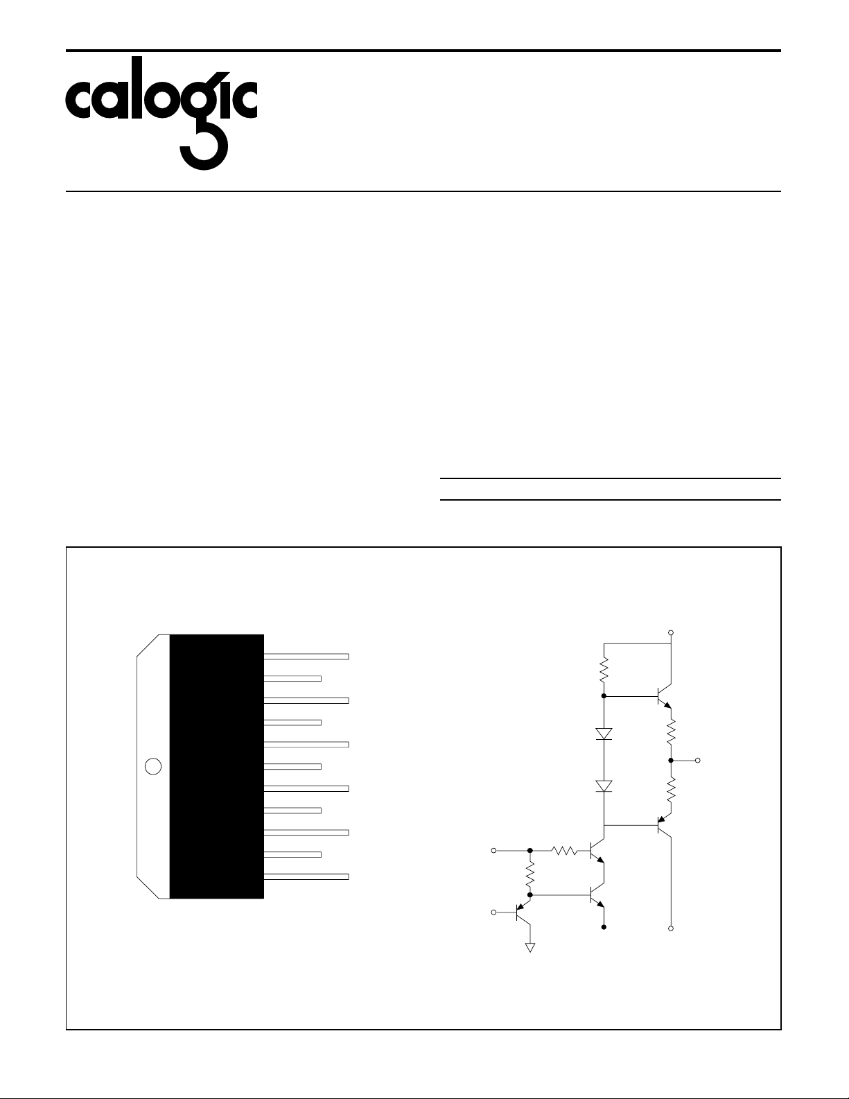
CONNECTION DIAGRAM AND SIM PLIFI ED SCHEM ATIC
TOP VIEW
T11A PACKAGE
11
10
9
8
7
6
5
4
3
2
1
GND = TAB
V
OUT
V
OUT
Gain/Peaking
Control
Gain/Peaking
Control
Gain/Peaking
Control
V
2
V
V
V
V
V
OUT
CC
3
BIAS
IN
IN
IN
1
3
2
1
P-P
1N-22
DESCRIPTION
The CVA2403T is a high input impedance wideband triple
amplifier. The device is specifically designed to drive a CRT
featuring a high speed buffer for easy matching to a pre-amplifier,
no crossover distortion for excellent gray scale linearity, external
emitter peaking to maximize the high frequency gain at the cross
hatch pattern and an adjustable gain for ease of use. This
device can drive monitors with resolutions of 1280 X 1024
(interlaced) with pixel frequencies of 220MHz.
The part is housed in the industry standard 11-lead TO-220
molded power pack age. The heat sink is gr ounded.
ORDERING INFORMATION
Part Package Temperature
o
CVA2403T T11A -20
3
2
1
C to +100oC
CALOGIC CORPOR ATION, 237 Whitney Place, Fremont, California 94539, Telephone: 510-6 56-290 0, FAX: 510-651-3025
Page 2

CVA2403T
GND
TAB
1P-39
V
IN
V
BIAS
C1 = 0.01µF
C2 = 100
µ
F
C3 = 0.1
µ
F
C7 = 120pF
D1, D2 = FHD400
R1 = 62
Ω
R2 = 20
Ω
C4 = 100µF
C6 = 8pF
R2
R1
C6
C4C3
C2C1
D2
D1
VIDEO
INPUT
V 9
CC
1,3,5
7
8,10,11
V
OUT
C7
V
PG
2,4,6
TEKTRONIX
FET PROBE
MODEL 620 1
(CAP. 1.5pF)
CVA2403T
ABSOLUTE MAXIMUM RATINGS
Supply Voltage. . . . . . . . . . . . . . . . . . . . . . . . . . . . . . . . . . 90V
Power Dissipation . . . . . . . . . . . . . . . . . . . . . . . . . . . . . . . 16W
Storage Tempera tu re. . . . . . . . . . . . . . . . . . . -25
o
C to +100oC
CORPORATION
Operating Temperature . . . . . . . . . . . . . . . . . -20
o
C to +100oC
Lead Temperat ure . . . . . . . . . . . . . . . . . . . . . . . . . . . . +300
o
C
DC ELECTRICAL CHARACTERISTICS Vs = 80V, CL = 8pF, DC
INPUT BIAS
= 12V, VIN = 3.4V, V
OUT
= 50V
p-p
. T
CASE
= +25oC.
See Figure 1.
SYMBOL CHARACTERISTICS MIN TYP MAX UNITS
I
cc
V
OUT DC
A
v
AC ELECTRICAL CHARACTERISTICS Vs = 80V, CL = 8pF, DC
Supply Current 30 34 40 mA
Output DC Level 40 45 50 V
Voltage Gain 13 15 17 V
Gain Matc h ing 0.2 dB
INPUT BIAS
= 12V, VIN = 3.4V, V
OUT
= 50V
p-p
. T
CASE
= +25oC.
See Figure 1.
SYMBOL CHARACTERISTICS MIN TYP MAX UNITS
T
r
T
f
L
e
OS Overshoot 5 %
Rise Time 4 4.5 ns
Fall Time 44.5ns
Linearity 6%
FIGURE 1. TEST CIRCUIT
CALOGIC CORPOR ATION, 237 Whitney Place, Fremont, California 94539, Telephone: 510-6 56-290 0, FAX: 510-651-3025
Page 3

CORPORATION
1P-40
GND
TAB
V
BIAS
C1 = 0.01µF
C2 = 100
µ
F
C3 = 0.1
µ
F
C4 = 100
µ
F
C5 = 2.2
µ
F
C7 = 40 - 120pf
D1, D2 = FHD400
L = 330 - 390nH
R1 = 62
Ω
R2 = 20
Ω
R3 = 47
Ω
R4 = 47(1/2W)
Ω
R7 = 33
Ω
R8 = 39
Ω
R10 = 680
Ω
R3
R4
C4C3
C2C1
D2
D1
V 9
CC
7
8,10,11
V
OUT
C5
SPARK
GAP
CVA2403T
R5
L
V
IN
R2
R1
VIDEO
INPUT
1,3,5
C7
V
PG
2,4,6
DC BIAS
FIGURE 2. APPLICATION CIRCUI T
CVA2403T
APPLICATION INFORMATION
The CVA2403T is a high voltage triple CRT driver suitable for
VGA, Super VGA, IBM
®
8514, 1280 x 1024 and 1024 x 768
non-interlaced display applic ations. The CVA2403T features
80V operation. The part is housed in the industry standa rd 11
lead TO-220 mo lded p ower package. The he at sink is flo at in g
and may be grounded for ease of manufacturing and RFI
shielding.
Thermal Considerati ons
The transfer characteristics of the amplifier are shown in
Figure 4.
current increases as the input signal increases and
consequently power dissipation also increase s.
The CVA2403T cann ot be used withou t heat sinking.
shows the power dissipated in each channel over the
operating voltage range of the device. Under white screen
conditions, i.e.: 20V output, dissipation increases to 16W
total. The CVA2403T case temperature must be maintained
below +90
is +50
equal to or less than:
R
The CV A 24 03T maximum load is 600 Ω to ground or V
The output of CV A2403T i s not shor t ci rc uit pr oof . Any r e sist ance
to V
Since this is a cl ass A input stage, power supply
o
C. If the maximum expected ambient temperature
o
C, then a heat sink is needed with thermal resistance
(90
− 50
=
th
16W
+
or Ground should be > 600Ω.
o
C)
= 2.5oC/W
Figure 2
+
.
FIGURE 3. CVA2403 T DC Chara cteristi cs
110
100
90
OUTPUT VOLTAGE (VOLTS)
80
70
60
50
40
30
20
10
0
1462
VOLTAGE POWER
357
INPUT VOLTAGE
6
POWER DISSIPATION (WATTS)
5
4
3
2
1
1G-26
CALOGIC CORPOR ATION, 237 Whitney Place, Fremont, California 94539, Telephone: 510-6 56-290 0, FAX: 510-651-3025
Page 4

CVA2403T
TYPICAL CHARACTERISTIC S
WITH PEAKING
30V
INDUCTOR & CAPACITOR
RISE TIME
30V
FALL TIME
WITH PEAKING
INDUCTOR & CAPACITOR
CORPORATION
8V/DIV
10V
90V
8V/DIV
10V
120.5V
10ns/DIV
RISE TIME
WITH PEAKING
CAPACITOR (NO INDUCTOR)
10ns/DIV
RISE TIME
NO PEAKING
INDUCTOR OR CAPACITOR
1D-02
1D-04
8V/DIV
10V
90V
8V/DIV
10V
120.5V
10ns/DIV
FALL TIME
WITH PEAKING
CAPACITOR (NO INDUCTOR)
10ns/DIV
FALL TIME
NO PEAKING
INDUCTOR OR CAPACITOR
1D-03
1D-05
10V/DIV
2.5V
10ns/DIV
Inform at ion furni shed by Calogic is believed to be accurate and reliable. Howe ver, no responsibility is assum ed for its use: nor for any in fring eme nt of pate nts or other
rights of third parties which may result from its use. No license is granted by implication or otherwise under any patent rights of Calogic.
1D-06
10V/DIV
2.5V
10ns/DIV
1D-07
CALOGIC CORPORATION, 237 Whitney Place, Fremont, California 94539, Telephone: 510-656-2900, FAX: 510-651-3025
Page 5

CORPORATION
CVA2401T
 Loading...