

Page 1
CORPORATION
CRT Driver
+ DC Bias Amplifier
Preliminary Data Sheet
CVA1775N
FEATURES
•• Little or No Heat Sink Required
•• Ease of Use
•• Rise Time . . . . . . . . . . . . . . . . . . . . . . . . . . . . . . . . . . <8ns
•• Fall Time. . . . . . . . . . . . . . . . . . . . . . . . . . . . . . . . . . . <7ns
APPLICATIONS
•• 14", 15", 17" Monitors wi th 70KHz Scan ning Fr eque ncy
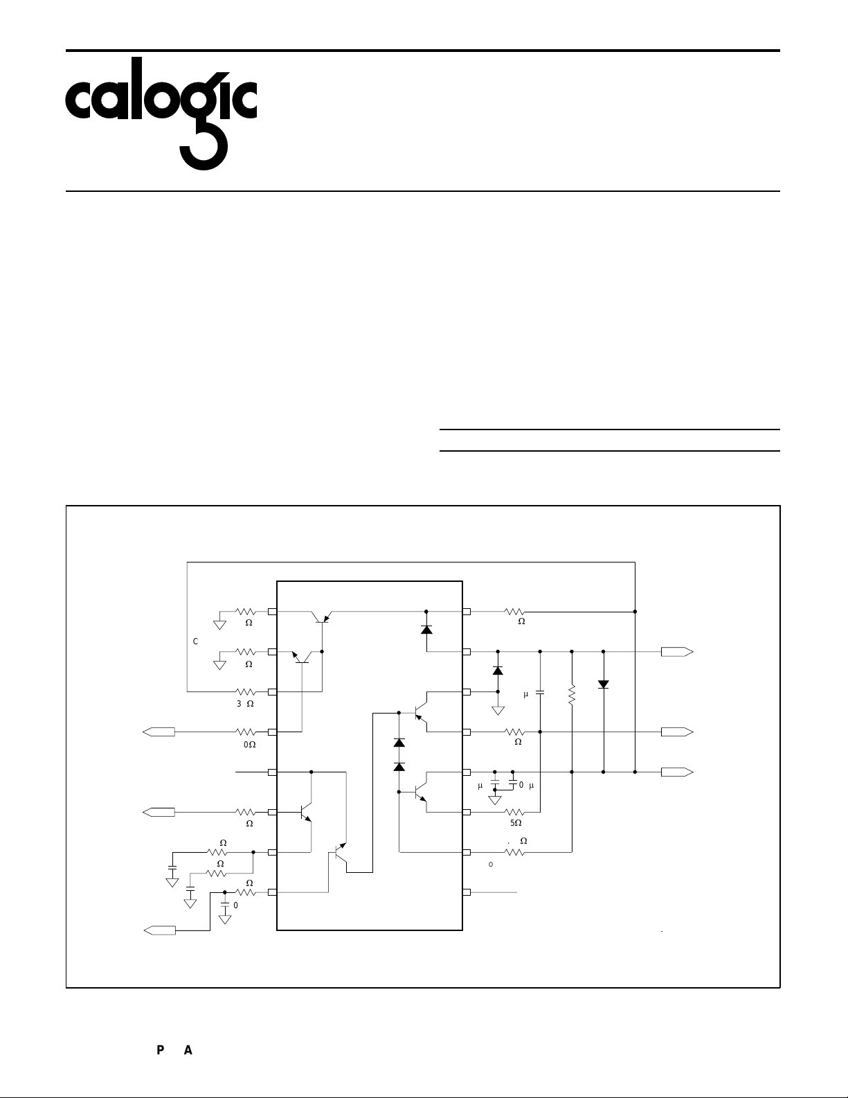
SCHEMA T IC, TEST CIRCUIT
GND-CUTOFF
CUTOFF-GAIN (L)
CUTOFF-GAIN (H)
IN-CUTOFF
V (VIDEO)
IN
R
GAIN
100
47
27pF
W
W
2K
2K
33K
100
33
47
.010pF
1
W
2
W
3
W
4
W
5
6
W
7
W
8
CVA1775N
DESCRIPTION
The CVA1775N includes a cascode CRT driver and a DC bias
cutoff amplifier. All of the active components are inside the
CVA1775N. Only the passive components and protection diodes
are needed t o drive a CRT tube. The CVA1775N can easily
drive 70KHz monitors. With the unique feature of DC bias
circuitry the print ed circuit board will shrink as EMI performance
will be improved.
ORDERING INFORMATION
Part Package Temperature
o
CVA1775N 16-PDIP 0
16
BIASED-CUTOFF
W
33K
BIASED-CUTOFF
15
14
13
12
10mF .01mF
11
10
9
1
m
F
W
15
W
15
1.5K
W
R
LOAD
1M
C to +1 1 0oC
V TO CRT
OUT
V (DRIVER)
OUT
V (80V)
CC
V (12V)
BIAS
1U-21
CALOGIC CORPOR ATION, 237 Whitney Place, Fremont, California 94539, Telephone: 510-6 56-290 0, FAX: 510-651-3025
Page 2
CVA1775N
ABSOLUTE MAXIMUM RATINGS
Supply Vo ltage (Driver Pin #12) . . . . . . . . . . . . . . . . . . . 100V
Supply Voltage (cutoff ) . . . . . . . . . . . . . . . . . . . . . . . . . . 250V
Storage Tempera tu re. . . . . . . . . . . . . . . . . . . -25
o
C to +125oC
CORPORATION
Junct i on Temperature . . . . . . . . . . . . . . . . . . . . . . . . . . 175
Operating Temperature ( Cas e) . . . . . . . . . . . . . 0
o
C to +1 1 0oC
Lead Temperature . . . . . . . . . . . . . . . . . . . . . . . . . . . . +300
o
C
o
C
CRT DRIVER DC ELECTRICAL CHARACTERISTICS Vs = 80V, CL = 12pF , V
= 12V, VIN = 2.7V, RL = 1500Ω, T
BIAS
CASE
= +25oC.
SYMBOL CHARACTERISTICS MIN TYP MAX UNITS
I
cc
V
OUT DC
A
(Driver) Voltage Gain 13 15 V
v
CRT DRIVER AC ELECTRICAL CHARACTERISTICS Vs = 80V, CL = 12pF, V
Supply Current 20 26 mA
Output DC Level 44 50 56 V
= 12V, VIN = 2.7V, RL = 1500Ω, T
BIAS
CASE
SYMBOL CHARACTERISTICS MIN TYP MAX UNITS
T
r
T
f
L
e
Rise Time 7.5 9 ns
Fall Time 7.5 9 ns
Linearity 5%
OS Overshoot 3 %
BIAS AMPLIFIER DC ELECTRICA L CHARACTERI STICS Supply Voltage = 150V , VB = 12Vsee test circuit .
SYMBOL CHARACTERISTICS TYP MIN MAX UNITS CONDITIONS
I
CC
V
OUT(LOW)
V
OUT(HIGH)
Gain Voltage Gain 13.8 12 16 V/V ∆V
∆ Gain Gain Match 0.5 1 dB Note 1
Supply Current 5 5.5 mA VIN = 5V
Output Voltage666070VV
IN
= 5V
Output Voltag e 121 118 126 V VIN = 1V
OUT
= +25oC.
/∆V
IN
Note 1. Calculate from voltage gain of each channe l.
Note 2: V
at VIN = 5V, ∆T = 25oC 100oC
OUT
CALOGIC CORPOR ATION, 237 Whitney Place, Fremont, California 94539, Telephone: 510-6 56-290 0, FAX: 510-651-3025
Page 3

VIN(VOLTS)
V
OUT
(VOLTS)
80
70
60
50
40
30
20
10
0
2
1.8
1.6
1.4
1.2
1.0
0.8
0.6
0.4
0.2
0
-0.2
0
0.2
0.5
0.7
1.0
1.2
1.5
1.7
2.0
2.2
2.5
2.7
3.0
3.2
3.5
3.7
4.0
4.2
4.5
4.7
5.0
5.2
5.5
5.7
6.0
V
OUT
Q3-POWER
POWER/OUTPUT STAGE
1T-25
1S-50
20ns/DIV
10V/DIV
FALL TIME
-2.75V
7.25V
1T-02
20ns/DIV
10V/DIV
CROSS HATCH
BLACK BACKGROUND
-1.75V
8.25V
CORPORATION
CVA1775N
APPLICAT ION INFORMATION
The CVA1775N is a high voltage driver and DC bias amplifier
suitable for VGA, Super VGA, IBM
®
8514, 1024 x 768
non-interlaced display applications. The CVA1775N features
80V and low power dissipation. The part is housed in the
industry standard 16- pin PDIP.
Thermal Considerati ons
The transfer characteristics of the CVA1775N application are
shown in
Figure 1.
Since this is a class A input stage, power
supply current increases as the input signal increases and
consequently power dissipation also increase s.
The CVA1775N can be used without a heat sink. Under white
screen condition, i.e. 25V output, dissipation is 0.6W/channel.
Under gray level conditions C
=12pf, V
L
OUT
= 45
P-P
, the
dissipation is 1.1W/channel.
The output of CVA1775N is not short circuit proof.
TYPICAL CHARACTERISTIC S
7.25V
RISE TIME
FIGURE 1. CVA1775 N DC CHARACTERISTI CS
10V/DIV
-2.75V
20ns/DIV
1S-49
CROSS HATCH
8.25V
WHITE BACKGROUND
10V/DIV
-2.75V
Inform at ion furni shed by Calogic is believed to be accurate and reliable. Howe ver, no responsibility is assum ed for its use: nor for any in fring eme nt of pate nts or other
rights of third parties which may result from its use. No license is granted by implication or otherwise under any patent rights of Calogic.
20ns/DIV
1T-01
CALOGIC CORPORATION, 237 Whitne y Place , Fremont, California 94 539, Telephone: 510-656-2900, FAX: 510-651-3025
 Loading...