

Page 1
CORPORATION
OUT
OUT
11
10
9
8
7
6
5
4
3
2
1
IN
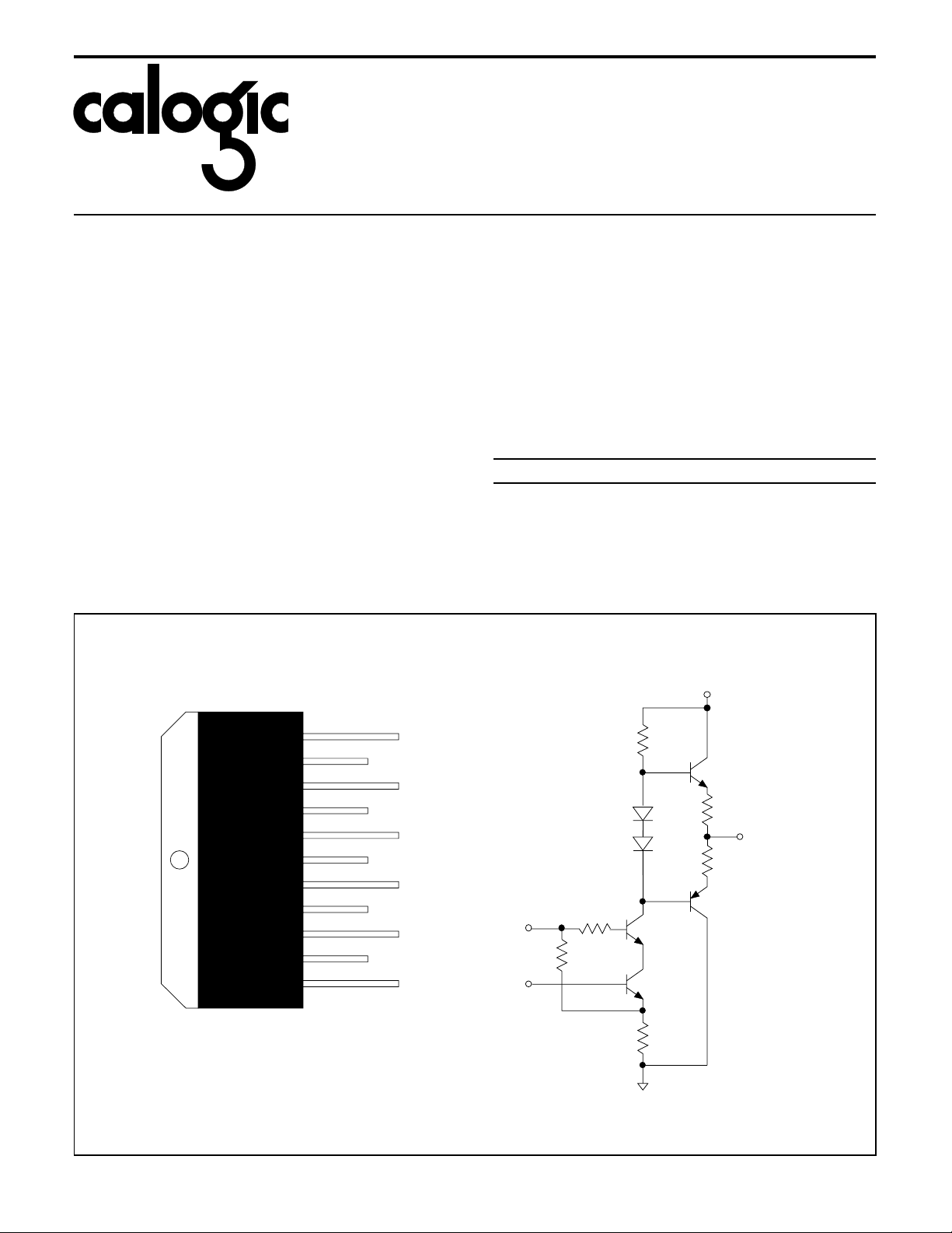
TOP VIEW
T11A PACKAGE
V 2
V 1
V
V 2
BIAS
V
CC
1L-38
OUT
V 3
IN
V 3
IN
V 1
GND
GND
GND
1T-18B
6
V
CC
1,3,5
V
O
11,9,8
V
IN
7,4,2,TAB
10
V
BIAS
Triple CRT Driver
Preliminary Product Information
CVA1405T
FEATURES
•• Rise/Fall Time (at th e Cat hode ) . . . . . . . . . . . . . . . . 9.0ns
•• Swing . . . . . . . . . . . . . . . . . . . . . . . . . . . . . . . . . . . 65V
P-P
•• Supply Voltage. . . . . . . . . . . . . . . . . . . . . . . . . . . . . . 100V
•• Pin to Pin Compatible to CVA2404T
APPLICATIONS
•• CRT driver for up to 64kHz monitor s with resolutio n up
to 1024 x 768
CONNECTION DIAGRAM
DESCRIPTION
The CVA1405T contains three wideband amplifiers, designed
specifically to drive a CRT. The device can drive monitors with
resolutions up to 1024 x 768 (n on-int erlaced) .
The product is housed in the industry standard 11 lead
TO-220 m olded power package.
ORDERING INFORMATION
Part Package Temperature
o
CVA1405T T11A -20
C to +100oC
CALOGIC CORPOR ATION, 237 Whitney Place, Fremont, California 94539, Telephone: 510- 656- 2900, FAX: 510-651-3 025
Page 2
CORPORATION
ABSOLUTE MAXIMUM RATINGS
Supply Voltage. . . . . . . . . . . . . . . . . . . . . . . . . . . . . . . . . 100V
Storage Tempera tu re. . . . . . . . . . . . . . . . . . . -25
o
C to +125oC
CVA1405T
Operating Temperature . . . . . . . . . . . . . . . . . -20
Lead Temperature . . . . . . . . . . . . . . . . . . . . . . . . . . . . +300
o
C to +100oC
o
C
DC ELECTRICAL CHARACTERISTICS Vs = 80V, DC
INPUT BIAS
= 12V, VIN = 2.5V, T
CASE
= +25oC.
See Figure 1.
SYMBOL CHARACTERISTICS MIN TYP MAX UNITS
I
cc
V
OUT DC
A
v
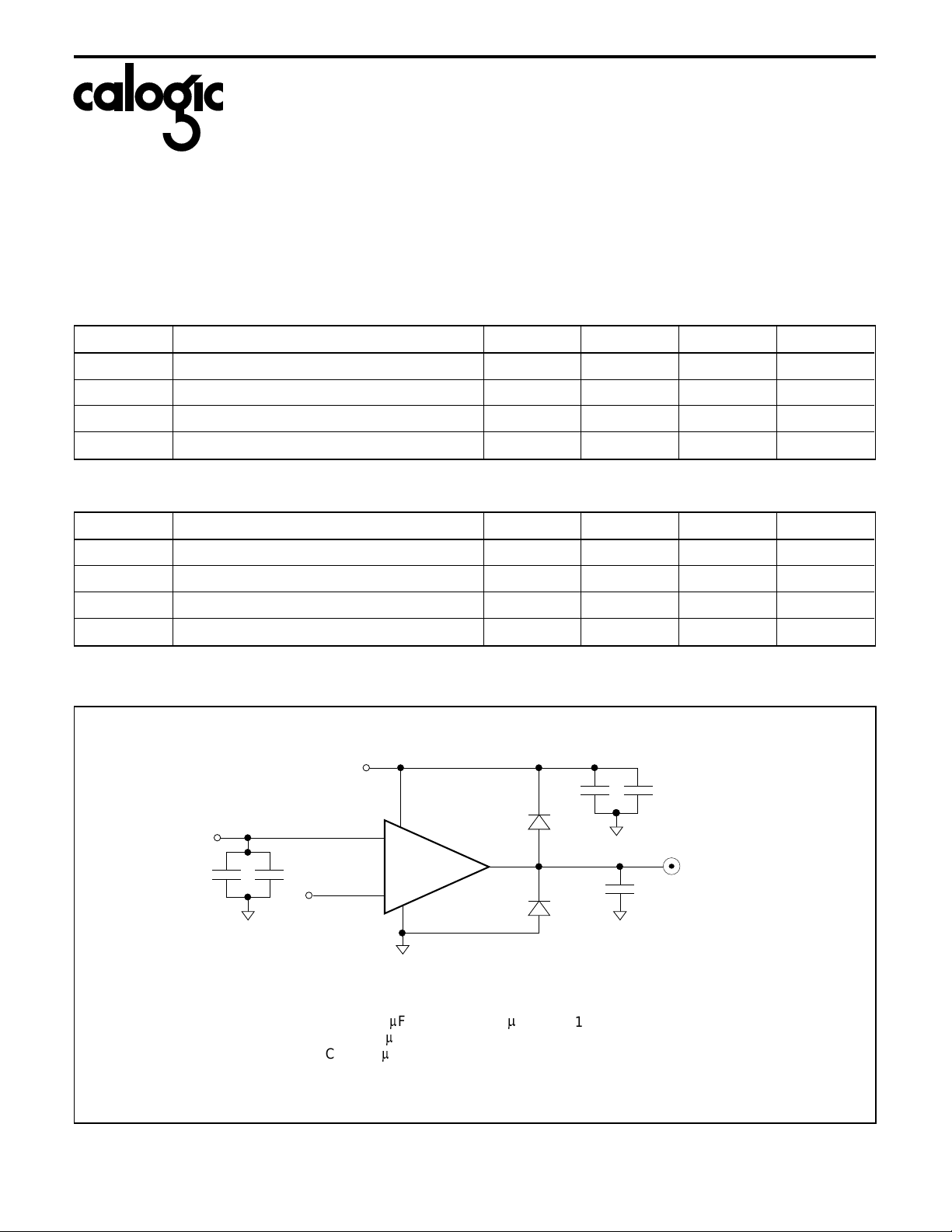
AC ELECTRICAL CHARACTERISTICS (at the cathode) Vs = 80V, CL = 8pF, DC
T
= +25oC. See Figure 1.
CASE
SYMBOL CHARACTERISTICS MIN TYP MAX UNITS
T
r
T
f
L
e
OS Overshoot/Undershoot 3 %
Supply Current @ 1MHz 15 18 mA
Output DC Level 50 54 58 V
Voltage Gain 13 15 17 V
Gain Matching 0.2 dB
INPUT BIAS
Rise Time 9 11 ns
Fall Time 911ns
Linearity 5%
= 12V, VIN = 2.4V, V
OUT
FIGURE 1. TEST CIRCUIT
= 50V
p-p
.
V
CC
C4C3
V
BIAS
C2C1
VIDEO
INPUT
10
V
IN
11,9,8
6
CVA1405T
7,4,2
V
OUT
1,3,5
D1
D2
C6
TEKTRONIX
FET PROBE
MODEL 6201
(CAP. 1.5pF)
GND,TAB
C1 = 0.01mF
m
C2 = 100
C3 = 0.1
F
F
m
C4 = 100
C6 = 8pF
F
m
D1, D2 = FHD400
1T-38
CALOGIC CORPOR ATION, 237 Whitney Place, Fremont, California 94539, Telephone: 510- 656- 2900, FAX: 510-651-3 025
Page 3

1T-39
V
BIAS
VIDEO
CVA1405T
+80V
L
R
91
W
SPARK
GAP
33
W
CORPORATION
FIGURE 2.
FIGURE 3.
CVA1405T
+80V
V
BIAS
VIDEO
CVA1405T
1K
APPLICATION INFORMATION
The CVA1405T is a high voltage triple CRT driver suitiable to
drive 69kHz, 1024 x 768 CRT displays. It features a high
impedance input to match any pre-amplifier. The CVA1405T
has a true class AB output stage that results in excellent gray
scale linearity and consisten t EMI per for mance .
As with any high speed amplifier used in CRT display
applications, specific precaution should be taken to get the
required performance. Power supply should be by pass as
close to the device pin as possible. Use 0.01µf very near to
the device and a large capacitor of 10µf or more (preferable
100µf) near the device. A 0.1µf and 10µf should be connected
near the V
pin (#10). Arc protection is very essen tial. Fast
bias
diodes together with the spark gap will achieve sufficient
protection. However, in certain applications depends on the
tubes a high value of resistor is required to reduce the current
into the CVA1405T during arcing. This will result in less than
desireable performance some of which can be restored by
using a peaking inductor at the output pin,
Figure 2
. Another
way to achieve this is by using a RC network at the output of
the device and use a peak ing in duct or at the tube,
The rise and fall time of the CVA1405T may suffer due to
stray capacitances associated with the PC Board and other
components. It can be improved by carefully designing the
PC Board where the output stage and input stage ground path
Figure 3
L
R
C
CVA4502
DC BIAS
I.C.
BIAS
33
W
V
cc
SPARK
GAP
1T-46
are seperated. Calogic will assist customers in the layout of
the PC Board that will result in quick EMI passage and better
performance. The output peaking should be used only to
restore the performance loss due to stray capacitances. Over
peaking will cause excessive ringing that will have better
results but poor EMI. The DC restore circuit is also important
when considering the high frequency performance. Using
CVA4502, DC Bias IC, better results can be obtained and
high frequency pe rfor ma n ce can be maximixed.
THERMAL CONSIDERATIONS
Power supply current increases as the input signal increases
and consequen tly po wer dissipat ion also incr ea ses.
The CVA1405T cannot be used without heat sinking. The
calculations below shows the power dissipated in each
channel over the operating voltage range of the device.
Under white screen conditions, i.e.: 25V output, dissipation
increases to 8.1W total. The CVA1405T case temperature
must be maintained below +100
ambient temperature is +50
.
with thermal resistan ce equal to or less than :
R
=
th
(100 − 50
8.1W
o
C)
= 6.2oC/W
o
C. If the maximum expected
o
C, then a heat sink is needed
The output of CVA2405T is not short circuit proof.
CALOGIC CORPOR ATION, 237 Whitney Pla ce, Fremont, California 94539, Telepho ne: 510- 656- 2900, FAX: 510-651 -3025
Page 4

CORPORATION
1T-43
20ns/DIV
1V/DIV
FALL TIME
-2V
8V
-55.6ns
144.4ns
1T-44
20ns/DIV
1V/DIV
CROSS HATCH
BLACK BACKGROUND
-2V
8V
-55.6ns 144.4ns
FIGURE 4. APPLICATION CIRCUIT
V
BIAS
R3
C2C1
VIDEO
INPUT
V
CC
10
V
11,9,8
CVA1405T
IN
6
7,4,2
GND,TAB
V
OUT
1,3,5
D1
D2
C5
DC BIAS
CVA1405T
C4C3
L
R4
R5
SPARK
GAP
TYPICAL CHARACTERISTIC S
8V
1V/DIV
-2V
-55.6ns 144.4ns
8V
RISE TIME
20ns/DIV
CROSS HATCH
WHITE BACKGROUND
R3 = 47
W
R4 = 47(1/2W)
R7 = 33
W
R8 = 39
W
R10 = 680
W
1T-42
W
C1 = 0.01mF
m
C2 = 100
m
C3 = 0.1
C4 = 100
C5 = 2.2
F
m
m
F
D1, D2 = FHD400
F
L = 330 - 390nH
F
1T-41
1V/DIV
-2V
-21.6ns
Inform at ion furni shed by Calogic is believed to be accurate and reliable. Howe ver, no responsibility is assum ed for its use: nor for any in fring eme nt of pate nts or other
rights of third parties which may result from its use. No license is granted by implication or otherwise under any patent rights of Calogic.
CALOGIC CORPORATION, 237 Whitne y Place, Fremont, Californi a 94539, Telephone: 510-656-2900, FAX: 510-651-3025
20ns/DIV
178.4ns
1T-45
 Loading...