

Page 1
CH1788
Surface Mount PLCC 2400bps Modem
2003 Cermetek Microelectronics, Inc. Page 1 Document No. 607-0018 Revision A2 (07/03)
INTRODUCTION
The CH1788 modem has the smallest footprint and
lowest profile of any commercially available full
function, FCC Part 68 approved 2400bps modem.
Utilizing a 68 pin PLCC form factor and requiring a
minimum amount of PCB space (0.95”x0.95”x
0.255”), the CH1788 affords the design engineer
maximum flexibility. The CH1788 provides two
external interfaces: a CCITT V.24 standard 5 volt
serial interface for routing directly to a UART; and a
TIP and RING interface for connection to the PSTN
telephone line. The CH1788 is compatible with
available industry communication software or may be
controlled with software commands via an embedded
microcontroller.
The CH1788 modem supports asynchronous
operation at 2400bps, 1200bps, and 300bps to both
Bell and CCITT standards. Each device is FCC
approved and Canadian DOT approvable. An FCC
label is supplied. The CH1788 also meets UL 1950
Edition 3 requirements.
The CH1788 family of modems operate from a 5 volt
DC supply (3.3 volt devices are available by special
order). The combination of low power operation, zero
power standby mode and small form factor make the
CH1788 an ideal choice for portable equipment
applications.
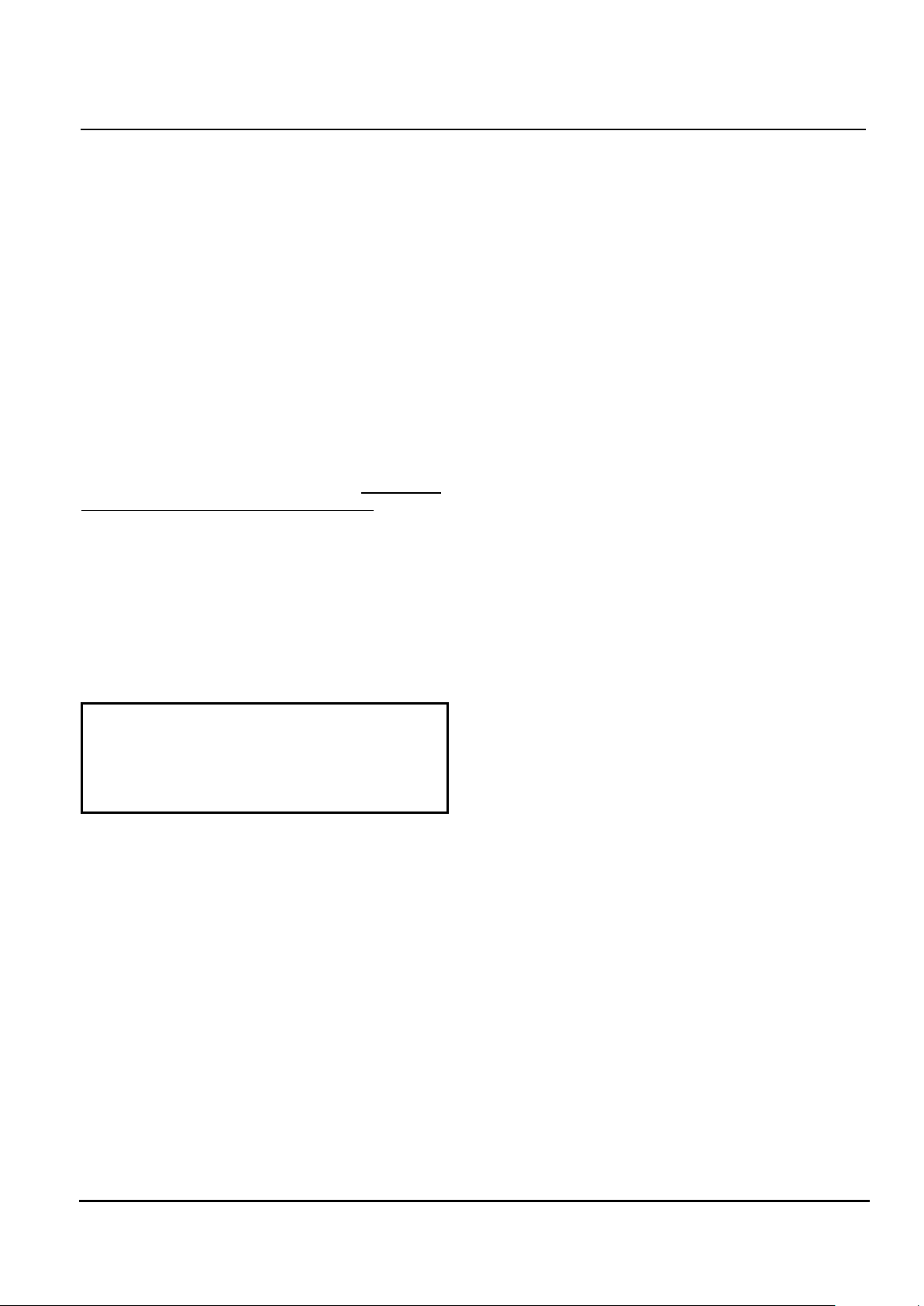
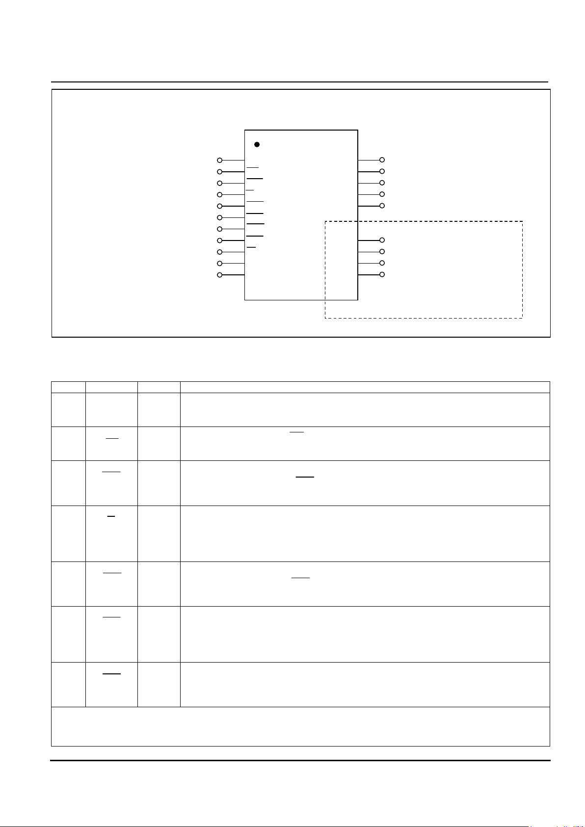
Figure 1. Functional Block Diagram of CH1788.
FEATURES
• Supports data rate standards, CCITT
V.22bis,V.22, Bell 212, and Bell 103, Bell 202,
V.23.
• Fast connect handshaking.
• FCC Part 68 approved and DOT CSA CS-03 Part I
approvable.
• UL 1950 and CSA C22.2 950 Listed.
• AT Command structure.
• Speed buffered operation at: 9600, 2400, 1200
and 300bps.
• Call progress tone detection.
• Caller ID information.
• Line In Use and Priority Pick Up 911 feature
support with external circuitry.
• DTMF generation and detection resident on
CH1788.
• 5 volt operation/ 3.3 volt operation available.
• Low power operation with automatic reduced
power idle and zero power standby modes.
• Low profile PLCC surface mount packaging; fits
standard 68 pin PLCC socket.
• Size: 0.95” x 0.95” x 0.255”(nominal).
CH1788 FAMILY
CH1788 Operating Temperature:
0°C to +70°C
CH1788ET Operating Temperature:
-40°C to +85°C
CH1788-3 3.3 volt Operation
Operating Temperature:
0°C to +70°C
CH1788-3ET 3.3 volt Operation
Operating Temperature:
-40°C to +85°C
DESCRIPTION OF FUNCTIONAL BLOCKS
AND DISCUSSION OF BASIC OPERATIONS
Figure 1 contains a functional block drawing of the
CH1788. The CH1788 is a highly integrated, fullfunction modem, comprised of a modulator/
demodulator, controller, and an FCC Part 68
approved telephone line interface.
Modulation/Demodulation and Modem Controller.
This function is provided by a monolithic modem
integrated circuit. The function is performed to CCITT
standards thereby making the CH1788 compatible
Page 2
Cermetek Microelectronics, Inc. CH1788 Surface Mount PLCC 2400bps Modem
2003 Cermetek Microelectronics, Inc. Page 2 Document No. 607-0018 Revision A2 (07/03)
with all modems. The ability to execute AT
commands is consistent with industry standards.
Telephone Line Interface or DAA. The CH1788 is
designed to meet 1500VAC RMS isolation and
provide 2122V peak surge protection. Consequently,
the CH1788 satisfies North American and some
international requirements. Note that supplemental
protection is required for FCC Part 68 conveyed
approval (see Figure 3 of this document). This
supplemental protection also improves field reliability
and facilitates FCC part 15 approval.
SUPPORTED FEATURES
AT Command Set. Internal to the CH1788 is an AT
command interpreter. AT commands and their
associated S-registers provide macro functionality.
These commands are summarized in this document
and are detailed in Cermetek publication CH1788 AT
Command and S-Register Reference Guide.
The CH1788 supports command concatenation. A
maximum of 63 characters (excluding AT) may be
included on each command line. S-registers provide
added programmability by allowing key parameters to
be configured for a specific application.
Serial Host Interface. The serial interface is a
standard TTL V.24 5V DC interface. It is functionally
similar to an RS232 interface.
IMPORTANT NOTE
Do not use RS232 interface voltage levels on the
serial pins. Damage may result. Adhere to the TTL
V.24 5V DC interface standard. See Schematic 7
for a suggested circuit to interface RS-232 logic to
the CH1788 TTL V.24 logic.
Command Characters. Each data byte or command
character consists of ten bits: 1 start bit, 1 stop bit,
and eight data bits. The data bits can be either eight
bits with no parity or seven odd or even with 1 parity
bit. The start bit is LOW going. RXD and TXD data is
non-inverted. See the pin descriptions in Table 2.
Data Encoding. The data encoding is user
configurable. The ATB command sets the decoding.
The following CCITT standards are supported:
V.22bis, V.22, Bell 212A, 103, Bell 202 or V.23.
Speed Buffered Mode. Speed Buffering allows the
serial data interface or DTE speed (i.e., the speed
between the host microcontroller and the CH1788) to
be fixed regardless of the connect or DCE speed (i.e.,
the speed between the CH1788 and the remote
modem).
The option exists to disable Speed Buffering by using
the ATY0 command. If Speed Buffering is disabled,
the data connection DCE speed will be equivalent to
the originating modems serial connection DTE speed.
In other words, disabling Speed Buffering forces the
answering modem to connect with a DCE speed
equivalent to the serial DTE speed of the originating
modem.
Data Transmission Speed. The CH1788 allows the
DTE speed to be set to 300, 1200, 2400, or 9600bps.
The DCE speed can be set to 2400, 1200, or 300bps.
A connect message will appear on RXD indicating the
connected data rate.
General Operation. By definition, the originating
modem initiates the PSTN connection and the
answering modem accepts the incoming call. The
connectivity speed (i.e., DCE speed) is determined by
the originating modem.
The originating modem’s DTE speed is established,
in turn, with an initializing AT command issued by the
application’s host controller. Speed Buffering allows
the CH1788 to communicate with the host controller
at a DTE speed that is greater than the connect DCE
speed.
Assuming that the default configuration of the
CH1788 has not been modified with the ATB or ATY0
commands, the answering modem will attempt to
connect to the originating modem at the highest
possible data rate supported by the originating
modem. The connection rate can be less than the
maximum of 2400bps, for example, if the PSTN line is
impaired in some way.
By default upon power up, the CH1788 DTE speed is
set to 9600bps and Speed Buffering is enabled.
Typical Implementation. In a typical
implementation, the CH1788 has a DTE speed of
9600bps and will connect to the remote modem at a
DCE speed of 2400bps. Speed Buffering allows the
CH1788 to negotiate the DCE speed independent of
the DTE speed. Data transfer to the host will be at
the DTE Speed Buffered rate of 9600bps. In this
case, flow control is not required.
It is possible for the DTE speed to be slower than the
DCE speed. For example, a serial interface DTE
speed of 1200 bps and a data rate DCE speed of
2400 bps. In this case, flow control must be
employed by the host to prevent buffer overflow and
lost data.
POWER DOWN
The CH1788 has two power down modes: idle power
standby and zero power standby.
Page 3
Cermetek Microelectronics, Inc. CH1788 Surface Mount PLCC 2400bps Modem
2003 Cermetek Microelectronics, Inc. Page 3 Document No. 607-0018 Revision A2 (07/03)
Idle Power Standby. In idle power standby mode,
power is switched off automatically by the CH1788
after a period of no activity and is restored
automatically by the CH1788 when activity is again
detected. Activity is defined as a change of status on
DTR, TXD, RST or on any of the other input pins or
an Incoming Ringing signal on TIP/RING. Idle power
mode transitions are transparent to the user.
Zero Power Standby. In applications requiring near
zero power during standby periods, the power may be
switched completely off to the CH1788. This is done
by issuing the AT@Z command or by toggling DTR
after the ATR5 command has been executed.
Normal operation is resumed by performing a 50
msec (minimum) hardware reset on the RST pin.
RING INDICATION
The CH1788 produces a low going 80 msec pulse on
the RI Pin when a valid Incoming Ring signal is
detected. By default, a valid ring signal must fall
within the 10-75 Hz range and have a cadence of 2
seconds on and 4 seconds off. Alternate frequency
ranges and ring cadence’s may be programmed.
CH1788 RESET
The CH1788 may be reset using any of the following
methods. Delay sending commands to the CH1788
for a period of 500 msec after reset has been
completed to allow the CH1788 time to properly
reconfigure.
Hardware Reset. Upon power-up or when power
cycling, the CH1788 will automatically generate an
internal reset pulse. However, if the power supply
comes up too slowly, or has a rise time greater than
50 msec, the internal reset detection circuitry may not
generate the hardware reset.
RST Pin. Initiate a reset externally anytime after the
power supply has stabilized by applying a 50 msec
TTL high reset pulse to the RST pin.
Software Reset. Execute the ATZ command while in
command mode.
DTR Pin. Toggle the DTR pin after executing the
ATR3 command while in command mode.
POWER SUPPLY
Although any standard 5 volt DC supply is
acceptable, the user should be aware that during the
course of normal operation the CH1788 decodes
analog data signals from the PSTN line that are in the
millivolt range. Steps must be taken by the user to
insure that power supply noise on all supply lines,
including ground, does not exceed 50 mV peak to
peak. Any frequency between 20 kHz and 150 kHz
must be less than 500 micro volts peak. If necessary,
use dedicated power and ground planes. Failure to
provide such operating conditions could cause the
CH1788 to malfunction or to function erratically.
Recommendation. To reduce the effects of supply
noise, it is recommended that by-pass capacitors be
placed on the power supply as close to the CH1788’s
supply input (i.e., Pin 20) as practical. A 10 µF
Tantalum capacitor in parallel with a 0.01 µF ceramic
is recommended.
DTMF TONE DETECTION
The CH1788 is capable of detecting DTMF tones
without external hardware.
Setup. Detection will only occur when the CH1788 is
Off-Hook and in the command mode.
DTMF Decoding. The ATJ6 command enables
DTMF decoding. Register S65 will contain the
decoded DTMF result. The S65 register must be
continuously interrogated by the host controller
because the decoded DTMF decimal value is only
present in S65 when the DTMF tones are present on
the PSTN line.
The full range of decoded DTMF decimal values are
listed in Table 1. If the S65 register contains zero, it
indicates that no DTMF tones are present. Note, the
S65 register will contain zero between DTMF tones.
Recommendation. Sample the S65 register at a
rate at least twice (2X) the fastest DTMF tone
periodic rate. DTMF tones typically have a cadence
of 70 msec on and 70 msec off. In this case, the S65
register should be sampled at least every 35 msec.
Table 1. DTMF Tone Conversion.
DTMF TONE DECIMAL VALUE
1 129
2 130
3 131
4 132
5 133
6 134
7 135
8 136
9 137
0 138
* 139
# 140
No Tone 0
DTMF TONE GENERATION
The CH1788 is capable of generating DTMF tones
without external hardware. DTMF tone generation is
Page 4
Cermetek Microelectronics, Inc. CH1788 Surface Mount PLCC 2400bps Modem
2003 Cermetek Microelectronics, Inc. Page 4 Document No. 607-0018 Revision A2 (07/03)
useful for signaling and is supplemental to the DTMF
dialing capability.
Setup. Generation will only occur when the CH1788
is Off-Hook, in the command mode and prior to
carrier generation.
DTMF Encoding. By default, the CH1788 generates
DTMF tones at a 70 msec on/off cycle The cycle can
be modified with register S11.
Issuing an ATDT command string with the desired
DTMF digits and terminating the command string with
a semicolon (;) will cause the CH1788 to immediately
enter command mode after dialing. Alternatively, the
command mode may be entered from the data mode
by issuing the escape sequence (+++) to the
CH1788.
Enter: ATDT1234567890*#;<CR>
Result: Sends the DTMF tones and returns to
command mode. DO not exceed 63
characters on the command line.
DTMF Tones may also be sent using external
circuitry via the voice injection port. See Schematic
2.
CALLER ID
The CH1788 will detect Caller ID (i.e., CID)
information. CID data, when supplied by the local
telephone service provider, is present between the
first and second ring signals. Valid CID data is
preceded by the “CID” designation. This feature is
enabled via register S95.
Setup. CID requires additional external circuitry. An
RC network must be added to the CH1788 V+ and Vpins. See Schematic 4 for details. Register S95
must be set to 8 (the default value) to receive the CID
information. Other caller ID options are available.
See the details of register S95.
Operation. Using the circuit in Schematic 4, monitor
the RI pin for the period between the first and second
ring signal. The decoded CID data will appear on
RXD.
LINE IN USE
The Line In Use (i.e., LIU) feature allows the CH1788
to signal the host when a shared PSTN line is in use.
When in use, the LINE IN USE status message will
appear on RXD and the CH1788 will NOT go OffHook. This feature is enabled via register S110.
Setup. The LIU feature requires additional external
circuitry. See Schematic 5. Additionally, register
S110 must be set to 243.
PARALLEL PICK-UP
The Parallel Pick-Up (i.e., PIU) feature allows the
termination of a CH1788 modem call in progress, and
then allows a standard phone instrument sharing the
same PSTN line to seize the line and obtain a dial
tone. When terminating the modem call, DCD will go
high, if enabled. The PPU-V status message appears
on RXD.
Setup. The Parallel Pick-Up feature requires external
circuitry. See Schematic 6.
Operation. The Parallel Pick-Up circuit detects the
incremental change in Off-Hook voltage on the PSTN
line when a parallel connected phone instrument
goes Off-Hook.
Failure To Detect. The detection circuit in the
CH1788 may not detect the Off-Hook condition for
select phone instruments because these phone
instruments do not change the Off-Hook voltage
sufficiently to allow detection.
There is also the possibility that two devices going
Off-Hook simultaneously may defeat the PPU
detection circuitry.
Recommendation. To avoid a Failure To Detect
condition, use of a prioritized scheme such as that
employed in the 911 Priority Pick-Up application
circuit described below is strongly suggested.
IMPORTANT NOTE
The Parallel Pick-Up feature should only be used in
non-critical applications and never used as a
substitute for the 911 Priority Pick-Up circuit.
911 PRIORITY PICK-UP
The 911 Priority Pick-Up (i.e., 911 PPU) feature
allows the CH1788 to give Off-Hook priority to any
telephone sharing the PSTN line with the CH1788.
Setup. The Parallel Pick-Up feature requires external
circuitry. See Schematic 6.
Operation. If a parallel connected phone instrument
goes Off-Hook while the CH1788 is Off-Hook, the
CH1788 will immediately disconnect to give priority to
the phone instrument.
IMPORTANT NOTE
To ensure that the 911 PPU feature works reliably
in all applications, the CH1788 must be the first
device on the installation’s PSTN line. All other
phone or higher priority instruments must be down
the line from the CH1788.
Page 5
Cermetek Microelectronics, Inc. CH1788 Surface Mount PLCC 2400bps Modem
2003 Cermetek Microelectronics, Inc. Page 5 Document No. 607-0018 Revision A2 (07/03)
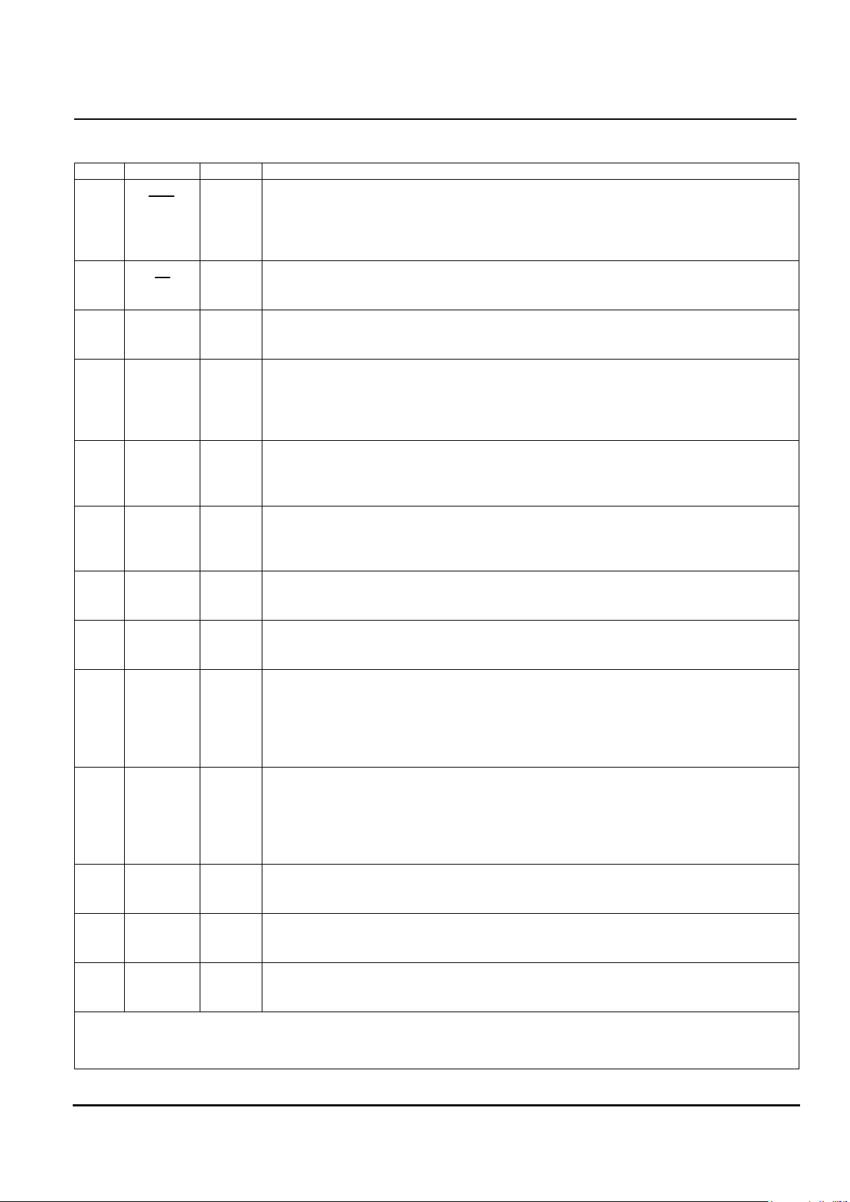
Figure 2. CH1788 Pin Configuration. See Table 2 for detailed Pin Descriptions.
Table 2. CH1788 Pin Descriptions.
PIN NAME TYPE FUNCTION
1
A1
O
Optional Input. Active high. Used when implementing the 911 Priority Pick-Up
circuit or the Line In Use circuit.
2
OH
O
Off-Hook. Active low. OH Indicates when the CH1788 is Off-Hook. Used in Line
In Use, 911 Priority Pick-Up applications and for Audio Control.
3
RTS
I
Request To Send. Active low. Used for optional flow control. Used in conjunction
with the Clear to Send (CTS) pin as a handshaking signal. See the details of
register S90.
4
RI
O
Ring Indication. Active low. For each occurrence of a valid ring signal, this pin will
pulse low for 70 ms. This output signal follows the frequency of the ringing signal
and is typically in the 20 to 40 Hz range with a cadence of 2 seconds on with 4
seconds off.
5
CTS
O
Clear to send. Active low. Used for optional flow control. Used in conjunction with
the Request To Send (RTS) pin as a handshaking signal. See the details of
register S90.
6
DSR
O
Data Set Ready. Active low. A low indicates that handshaking with the remote
modem is in progress and/or the carrier of the remote modem has been detected
and a valid connection is imminent as measured by DCD being active. This feature
is enabled with the N command.
7
DCD
O
Data Carrier Detect. Active low. This output must be enabled with the C
command. When enabled, it will become active when both the originated and
answering modems are connected and a data carrier has been detected.
NOTE: 1. All unused pins should be left unconnected when not required in a specific application,
unless specifically directed otherwise.
2. See DC characteristics before attempting to drive an LED directly from the output of any pin.
Used for LIU/911/Audio Control
CH1788
Top View
A1
OH
RTS
RI
CTS
DSR
DCD
DTR
A2
TXD
RST
RXD
GND
V
CC
S2
S1
V-
V+
TIP
RING
1
2
3
4
5
6
7
8
15
14
13
12
22
21
20
19
9
10
11
18
DTE Signal
Power Input +5V
DTE Si
g
nal
Optional S1/S2 Audio
Monitor/Tone/Voice
V+/V- Optional
CID Input
Telephone Line
Input
Hi
g
h Voltage Section
Used for LIU/911/General IO
DTE Si
g
nal
DTE Si
g
nal
DTE Si
g
nal
DTE Si
g
nal
DTE Si
g
nal
DTE Si
g
nal
Used for LIU/911/Detection
O
p
tional High Reset Input
Page 6
Cermetek Microelectronics, Inc. CH1788 Surface Mount PLCC 2400bps Modem
2003 Cermetek Microelectronics, Inc. Page 6 Document No. 607-0018 Revision A2 (07/03)
Table 2. CH1788 Pin Descriptions (Continued).
PIN NAME TYPE FUNCTION
8
DTR
I
Data Terminal Ready. Active low. The response to this input is controlled by the
Rn command where n specifies the desired options and includes: returning the
modem to the command state, hanging up the modem, resetting the modem, and
placing the modem in zero power mode.
9
A2
I
Optional Input. Active low. Used when implementing the 911 Priority Pick-Up
circuit or the Line In Use circuit.
10
TXD
I
Transmit Data. Serial transmit data input. Data starts with a high to low transition.
Mark or binary 1 condition is indicated by HIGH.
11
RST
I
Reset. Active HIGH. This input must be asserted HIGH for at least 50 ms to reset
the modem. The RST pin must be returned LOW for normal operation to
commence. If a system reset is not available, let this pin float to enable the internal
reset circuitry.
12
RING
I/O
Ring. Telephone connection requires an active public switched telephone line
(PSTN) for normal operation. This line should be routed to the RJ-11C jack through
the recommended protection circuitry.
13
TIP
I/O
TIP. Telephone connection requires an active public switched telephone line
(PSTN) for normal operation. This line should be routed to the RJ-11C jack through
the recommended protection circuitry.
14
V+
I
Caller ID. Used to connect an external RC network to enable caller ID operation.
See the application circuit in the Schematic 4.
15
V-
I
Caller ID. Used to connect an external RC network to enable caller ID operation.
See the application circuit in the Schematic 4.
18
S1
I/O
Audio Port. Optional audio port input. Allows the internal DAA to be shared with
external voice, tone injection or call progress monitoring applications. See the
application circuits in the Schematic 2 and 3. Note that the CH1788 is FCC
approved for data applications only. Inclusion of voice or other audio functions may
require additional certification by the FCC.
19
S2
I/O
Audio Port. Optional audio port input. Allows the internal DAA to be shared with
external voice, tone injection or call progress monitoring applications. See the
application circuits in the Schematic 2 and 3. Note that the CH1788 is FCC
approved for data applications only. Inclusion of voice or other audio functions may
require additional certification by the FCC.
20
V
CC
--
Power Supply. 5 Volt DC +/- 5%. Supply noise should be less than 50 mV
pp
. Also
available at for 3.3 volt DC operation, upon special request.
21
GND
-
Ground. Circuit ground. Use recommended bypass capacitors between GND and
VCC.
22
RXD
O
Receive Data. Serial receive data output. Data starts with a high to low transition.
Received mark or binary 1 condition is indicated by HIGH.
NOTE: 1. All unused pins should be left unconnected when not required in a specific application,
unless specifically directed otherwise.
2. See DC characteristics before attempting to drive an LED directly from the output of any pin.
Page 7
Cermetek Microelectronics, Inc. CH1788 Surface Mount PLCC 2400bps Modem
2003 Cermetek Microelectronics, Inc. Page 7 Document No. 607-0018 Revision A2 (07/03)
CALL PROGRESS MONITORING
Call Progress Monitoring allows a call to be monitored
during the dialing sequence. This feature becomes
active when the CH1788 goes Off-Hook and
automatically disables when DCD is detected. It is
also inactive if a connection attempt should fail and
the CH1788 goes back On-Hook. To enable this
feature, the DCD line must be activated with the
ATC1 command.
Setup. This feature requires additional external
circuitry. See Schematic 2. Although the circuit in
Schematic 2 uses a variable resistor to adjust the
speaker volume, a fixed value resistor may be
substituted.
Alternate Setup. Control of the speaker can
alternately be performed under command control. To
implement this alternate control method, modify the
circuit in Schematic 2 by connecting resistor R5 to A1
instead of DCD. This allows register S101 to be used
to turn the speaker on or off. Set S101 to 1 to turn
the circuit on, set S101 to 0 to turn the circuit off.
FAST CONNECT HANDSHAKING
The CH1788 supports a fast handshaking (often
called “quick connect”) feature. This feature is
controlled via the L3 command.
Typically, the initial handshaking sequence takes
between 10 and 20 seconds to complete. When fast
handshaking is selected, the handshaking sequence
will take between 4-8 seconds. Fast Connect
Handshaking will work with any compatible modem.
LONG SPACE DISCONNECT
The long space disconnect signal is used to force the
CH1788 to release the PSTN line and go back OnHook.
Setup. To enable this feature, bit 7 of register S110
most be set to 1. See the details of register S110.
VOICE INJECTION
It is possible to share the CH1788’s internal DAA with
external applications. This allows one PSTN line to
be shared between an external voice application and
the CH1788 modem. This feature is controlled via
register S101.
Setup. This feature requires additional external
circuitry. See Schematic 3. This application
implements Voice Injection via the S1 and S2 pins
and requires a two to four wire converter and a relay
circuit. Set S101 to 1 to activate Voice Inject and set
S101 to 0 to deactivate Voice Inject.
Operation. The two to four wire converter circuit
provides for simultaneous voice in and voice out (with
respect to ground). This circuit must be capacitor
coupled (i.e., C7) to the CH1788 and isolated from
ground (i.e., C6). Voice/data switching is controlled
by setting register S101 appropriately.
During Voice Injection, the voice signal must not
exceed 2.187 V
pp
(i.e., zero dB) per FCC maximum
permissible limits. When sending data, the voice
circuit must be fully disconnected from the line (i.e.,
Voice Inject deactivated) or data corruption will occur.
IMPORTANT NOTE
When utilizing the Voice Injection circuit, it is
necessary to submit the end product containing the
CH1788 Voice Injection feature to an FCC approved
testing facility for re-approval of the end product per
FCC Part 68 requirements.
MODEM CONTROL
The CH1788 may be controlled with ASCII AT
commands sequences. The commands are sent to
the CH1788 serially via the TXD pin. After execution
of a received command string, the CH1788 returns a
serial status message on RXD.
INITIALIZING THE MODEM
The CH1788 must be initialized before the CH1788
will recognize commands. Initialization is a two step
activity consisting of:
1. Hard Reset. This is accomplished by applying a
hardware reset pulse to pin RST for 50 ms. The
internal reset may be used by cycling the power.
The modem should not be accessed for 500
msec after a reset has occurred.
IMPORTANT NOTE
Delay the sending commands to the CH1788 for a
period of 500 msec after reset has been completed
to allow the CH1788 time to properly reconfigure.
2. Initial CH1788 Training. This will establish the
word bit length and type for communication with
the host. The word size should not be more than
10 bits including start and stop bits and is typically:
1 start bit, 1 stop bit, 8 data bits and with no parity.
The CH1788 is trained by the host with the
AT<CR>. The serial data rate (i.e., the DTE
speed) at which the host sends the AT<CR>
command initializes the modem DTE Speed.
3. The CH1788 S registers must be re-configured to
their required settings after a soft reset, hardware
reset, or power loss.
Page 8

Cermetek Microelectronics, Inc. CH1788 Surface Mount PLCC 2400bps Modem
2003 Cermetek Microelectronics, Inc. Page 8 Document No. 607-0018 Revision A2 (07/03)
4. Cermetek recommends issuing the following setup
string ATS13=39S73=176<CR> for best
performance.
THE COMMAND FORMAT
Typical commands consist of three elements: the
attention sequence, the commands themselves, and
a terminating carriage return.
AT[commands]<CR>.
Where: AT represents attention sequence.
[Commands] represents command strings.
<CR> represents carriage return (ASCII 13
or HEX 0D).
Training the Modem. The CH1788 must be trained
to set the DTE speed (i.e., to match its host’s speed
and parity) so that the CH1788 is able to recognize
serial asynchronous commands sent to it by the
host’s UART. The host must retrain the CH1788
each time a reset is performed.
Modem Training Command Sequence. The
CH1788 is trained by sending it the AT sequence:
Enter: AT<CR>
Result: OK
Where: A and T may be either upper or lower case
but must be the same case.
<CR> represents carriage return
The AT sequence is referred to as the attention
sequence. When received, the CH1788 will respond
with one of the following status messages, depending
on whether the CH1788 is optioned for Terse
(abbreviated) or Verbose (English) status messages.
Result: 0<CR> (Terse)
or
Result: <CR><LF>OK<CR><LF> (Verbose)
Where: <CR> represents carriage return (ASCII 13
or HEX 0D).
<LF> represents line feed (ASCII 10 or
HEX 0A).
After responding, the CH1788 will be in command
mode and ready to accept additional commands. An
alternate attention sequence A/ may be sent. This
command causes the previously entered command
string specified with the AT prefix to be executed.
AT Command Set. The available commands are
summarized in Table 5. Note that each command
may have several options and the options may be
influenced by various S-Register values. It is
recommended that the designer review Cermetek
publication CH1788 AT Commands and S-Registers
Reference Guide.
AT Command Structure. When issuing commands
to the CH1788, the backspace character-control-H
(ASCII 8 or HEX 08) may be used to perform
character editing.
Multiple commands may be placed on the command
line as long as the command line does not exceed 63
characters, excluding the letters AT. By way of
example, the command string below instructs the
CH1788 to configure itself to suppress character
echoing when in command mode E0 and then put
itself in the answer state A.
Enter: ATE0A<CR>
Result: OK
MODEM STATES
The CH1788 is in either of two states: command
mode or data mode. The CH1788 will only respond
to AT commands when it is in command mode.
When the modem is idle, by default it is in command
mode.
When data transmission is in progress, the CH1788 is
in data mode and will not recognize/respond to AT
commands. To cause the CH1788 to recognize
commands when in data mode, the host must send
an escape sequence to the CH1788 forcing the
CH1788 out of data mode and into command mode.
Only then will the CH1788 respond to AT commands.
If the CH1788 is Off-Hook, connected to a remote
modem and placed in command mode by its host, the
CH1788 will not transmit any commands received
from its host to the remote modem. However, when
in this state, the CH1788 will not receive data from
the remote modem.
Result Codes. After execution of an AT command
and at the completion of each dial attempt, the
CH1788 will deliver a status message on RXD.
Referring to Table 3, the message can be a Terse
(numeric) or Verbose (English) message. The
message type is controlled via the V command.
Various combinations of the listed result codes can
be selected with the W and X commands.
Escape Sequence. The escape sequence consists
of a “guard time” of one second (a period where no
characters are sent to the modem), followed by 3
escape characters (typically +++), followed by
another guard time of one second. The escape
character code is set in register S2. by default, the
escape character is set as “+.” There is no required
delay between characters. When the escape
sequence has successfully been sent, the escape
characters will not be transmitted to the remote
modem.
Page 9

Cermetek Microelectronics, Inc. CH1788 Surface Mount PLCC 2400bps Modem
2003 Cermetek Microelectronics, Inc. Page 9 Document No. 607-0018 Revision A2 (07/03)
Table 3. Summary of Common Result Codes and Meanings.
Standard Result Codes
Terse Verbose Meaning/Description
0 OK Command Executed
1 CONNECT Carrier detected at 300bps
2 RING Ring Detected
3 NO CARRIER Did not detect carrier
4 ERROR Entry error
5 CONNECT 1200 Carrier detected at 1200bps
6 NO DIAL TONE Off-hook, but no response after 5 seconds
7 BUSY Busy signal detected
8 NO ANSWER Remote modem did not answer
9 CONNECT 600 Connected, DTE to modem rate- 600bps
10 CONNECT 2400 Connected, DTE to modem rate- 2400bps
11 CONNECT 4800 Connected, DTE to modem rate-4800bps
12 CONNECT 9600 Connected, DTE to modem rate-9600bps
13 CONNECT 7200 Connected, DTE to modem rate-7200bps
14 LINE-IN-USE When attempting to go off hook on a busy line
22 CONNECT 75/1200 V.23 or Bell 202 - forward/reverse channel
Extended Result Codes
23 CONNECT 1200/75 V.23 or Bell 202 – forward /reverse channel
40 CARRIER 300 Modem (DCE) connect speed-300bps
41 CARRIER 600 Modem (DCE) connect speed-600bps
44 CARRIER 1200/75 Modem (DCE) connect speed-1200/75bps
45 CARRIER 75/1200 Modem (DCE) connect speed -75/1200bps
46 CARRIER 1200 Modem (DCE) connect speed-1200bps
47 CARRIER 2400 Modem (DCE) connect speed-2400bps
Page 10

Cermetek Microelectronics, Inc. CH1788 Surface Mount PLCC 2400bps Modem
2003 Cermetek Microelectronics, Inc. Page 10 Document No. 607-0018 Revision A2 (07/03)
The CH1788 will stay Off-Hook with its carrier on after
the escape sequence is received. It will return an OK
status message on RXD when it is ready to accept
commands. The CH1788 may be put into data mode
again by issuing the command ATO.
AT COMMAND APPLICATIONS
Dialing a phone number. The Dial command takes
the form Dn, where n is a string of characters. In the
simplest form, n will be the digits of the phone
number to be dialed.
Example: Dial number.
Enter: ATD1234567<CR>
Result: OK
In the above example, the CH1788 dials the
telephone number 1234567, conducts handshaking
negotiations then waits for a carrier from the distant
modem. If a carrier is not detected within the time
period specified by register S7, the CH1788 will
automatically release the PSTN line and send the
appropriate result code to the host. If a carrier is
detected, the CH1788 will send the CONNECT result
code and will permit communication with the distant
modem. Note, the CH1788 is ready to send and
receive data after the CONNECT result code is sent
or when an active signal is present on DCD. DCD
line must be enabled with the C1 command.
A variety of dial modifiers can be placed in the dialing
string to make it application specific. These include
pause, hook flash, pulse dialing, wait for dial tone,
etc. See the detailed D command.
The Dial Command may also be issued without a
telephone number. ATD causes the modem to pick
up the telephone line without dialing a number.
Programmable S-Registers. The CH1788 contains
a variety of registers that store the configuration and
personality parameters for the CH1788. Both default
configuration and user specified configuration
parameters are stored. A summary of the SRegisters is given in Table 4. A detailed description
of each is available in CH1788 Command and SRegister Reference Guide. Do not attempt to modify
S-Registers that are not listed in the table.
Table 4. CH1788 S-Register Summary.
Register Function
S0* Ring to Answer On
S1 Ring Count
S2 Escape Code Character
S3 Carriage Return Character
S4 Line Feed Character
S5 Back Space Character
S6 Wait for Dial tone
Table 4. CH1788 S-Register Summary
(Continued).
Register Function
S7 Wait for Data Carrier
S8 Pause Time for Comma
S9 Carrier Detect Response Time
S10 Lost Carrier to Hang-up Delay
S11 DTMF Tone On/Off
S13 DTMF Data/ Transmit Attenuation
S17 Ring Minimum Frequency
S18 Ring Maximum Frequency
S23 Call Progress Functions
S30 Data Modulation Selection
S31 Data Modulation Status
S51 Ring/ Cadence A minimum On-Time
S52 Ring/ Cadence A maximum On-Time
S53 Ring/ Cadence A minimum Off-Time
S54 Ring/ Cadence A maximum Off-Time
S55 Ring/ Cadence B minimum On-Time
S56 Ring/ Cadence B maximum On-Time
S57 Ring/ Cadence B minimum Off-Time
S58 Ring/ Cadence B maximum Off-Time
S65 DTMF Detection
S66 Wait For Dial Tone Timer
S67 Minimum Duration Of Dial Tone
S68 Test Timer
S69 Test Error Count
S86 Hook Flash On Time
S95 Caller ID configuration
S110 Line-In-Use/ Parallel Pick-Up
Register
S111 Line-In-Use Setting Time
Automatic Answering. Register S0 specifies the
number of rings that the CH1788 must detect before it
will answer. S0 may range in value from 0 to 255.
S0 =0 DO NOT ANSWER TELEPHONE
S0 =1 ANSWER ON RING 1
S0 =2 ANSWER ON RING 2
S0 =3 ANSWER ON RING 3
S0 =255 ANSWER ON RING 255
When S0 is set to 0, the modem will not answer.
IMPORTANT NOTE
The tables included in this data sheet are a summary
of the AT commands and S-Registers. A detailed
description of all commands and registers is available
from Cermetek Microelectronics, Inc., and should be
consulted prior to design. Refer to Cermetek
publication CH1788 AT Commands and S-Registers
Reference Guide or access our website at
http://www.cermetek.com.
Page 11

Cermetek Microelectronics, Inc. CH1788 Surface Mount PLCC 2400bps Modem
2003 Cermetek Microelectronics, Inc. Page 11 Document No. 607-0018 Revision A2 (07/03)
Table 5. CH1788 AT Command Set Summary.
Basic
Commands
Function
AT Attention Code
A Answer command
A/ Repeat last Command
C Carrier Detect DCD Signal Monitor
D Dial Command
E Off-Line Character Echo Option
H Switch Hook Control Option
I Identification Option
K DCE-DTE Flow Control
L Fast Connect Option
N Data Set Ready DSR Signal
Monitor
O On-Line Command
P Pulse Dial
Q Result Code Display Option
R Data Terminal Ready DTR Monitor
S S Register Monitor
T Tone Dialing
V Verbose / Numeric Result Codes
W Extended Result Codes
X Result Code Set/Call Progress
Y Async. Speed Buffered Option.
Z Reset
@T Test Modes
@Z Power Down
+++ Escape Sequence
PSTN LINE CONNECTION GUIDELINES
1. The CH1788 must be mounted in the final
assembly such that it is isolated from exposure to
any hazardous voltages within the assembly.
Adequate separation and restraint of cables and
cords must be provided.
2. The circuitry from the CH1788 to the telephone
line interface must be provided in wiring that
carries no other circuitry other than that
specifically allowed in the FCC rules.
3. Connection to phone line should be made
through an approved RJ-11C jack.
4. PCB traces from the modem’s RING and TIP pins
to the RJ-11C jack must be 0.1 inch spacing or
greater to one another and 0.2 inch spacing or
greater to all other traces. The traces should
have a nominal width of 0.020 inches or greater.
5. The RING and TIP PCB traces should be as
short as possible and oriented to prevent
coupling other high speed or high frequency
signals present on the host circuit PCB.
6. No additional circuitry other than that shown may
be connected between the modem module and
the RJ-11C jack. Doing so will invalidate the
FCC approval.
7. The CH1788 requires external surge protection.
This is mandatory to maintain FCC Part 68
conveyed approval. Please use only
recommended components and values. Do not
use an MOV or a Transorb.
8. The CH1788, the RJ-11C jack, the protection
circuitry and all PCB traces in between, must be
contained on a PCB with a 94 V-0 flammability
rating.
9. The supplied FCC registration label must be
applied visibly on the outside of the product.
10. The product’s User Manual must provide the user
with instructions for connection and use as
recommended in the FCC Registration Section
below.
CH1788 HANDLING AND ASSEMBLY
RECOMMENDATIONS
The CH1788 contains static-sensitive components
and should only be handled by personnel and in
areas that are properly protected against static
discharge.
Direct Soldering. The CH1788 may be wave
soldered. All CH1788 products are moisture resistant
and will not be harmed by industry standard wave
soldering processes. Cermetek recommends against
socketing the modem for production products.
However, for development purposes a 68 pin PLCC
socket may be used.
FCC REGISTRATION
The CH1788 is registered with the FCC (Federal
Communications Commission) under Part 68. To
maintain the validity of the registration, the end
product supplier must notify to the end user of the
product of several restrictions the FCC places on the
CH1788 and its use.
In addition to restriction notification, the FCC requires
that Cermetek make all repairs to the CH1788. If
repairs are necessary after installation of the CH1788
in the end product and the end product has been
delivered to the end user, the end product must be
returned to the end product supplier where the
CH1788 can be removed and then forwarded to
Cermetek for repair. The following notice is
recommended and should be included in the end
product’s user manual.
Page 12

Cermetek Microelectronics, Inc. CH1788 Surface Mount PLCC 2400bps Modem
2003 Cermetek Microelectronics, Inc. Page 12 Document No. 607-0018 Revision A2 (07/03)
FOR YOUR USER’S MANUAL
The FCC Part 68 rules require the following (or
equivalent) be provided to the end user of equipment
containing a registered element.
Type of Service. The (insert end product name) is
designed to be used on standard device telephone
lines. It connects to the telephone line by means of a
standard jack called the USOC RJ-11C (or USOC
RJ45S). Connection to telephone company provided
coin service (central office implemented systems) is
prohibited. Connection to party lines service is
subject to state tariffs.
Changes in Attestation Procedure for Plugs and
Jacks. (Name of applicant) attests that the network
interface plugs or jacks used on this equipment
comply with and will continue to comply with the
mechanical requirements specified in Part 68, subpart F, specifically the dimensions, tolerances and
metallic plating requirements. The compliance of
these connectors will be assured by purchase
specifications and incoming inspection.
Documentation of such specifications and/or
inspections will be provided to the FCC within 30
days of their request for same.
Telephone Company Procedures. The goal of the
telephone company is to provide the best service it
can. In order to do this, it may occasionally be
necessary for them to make changes in their
equipment, operations or procedures. If these
changes might affect the service or the operation of
equipment, the telephone company will provide
notice, in writing, to allow time to make any changes
necessary to maintain uninterrupted service.
In certain circumstances, it may be necessary for the
telephone company to request information from you
concerning the equipment which you have connected
to your telephone line. Upon request of the
telephone company, provide the FCC registration
number and the ringer equivalence number (REN);
both of these items are listed on the equipment label.
The sum of all of the REN’s on your telephone lines
should be less than five in order to assure proper
service from the telephone company.
If Problems Arise. If any telephone equipment is not
operating properly, it should immediately be removed
from the PSTN line, as it may cause harm to the
PSTN network. If the telephone company notes a
problem, they may temporarily discontinue service.
When practical, they will provide notification in
advance of this disconnection. If advance notice is
not feasible, notification will be made as soon as
possible.
If notified, the telephone company will allow the
opportunity to correct the problem and will
acknowledge your right to file a complaint with the
FCC. Contact the local telephone service provider
with any questions about the local PSTN line.
In the event repairs are ever needed on the (insert
your product name), they should be performed by
(insert your company name) or an authorized
representative of (insert your company name). For
information contact: (insert your company address).
DEFAULT STATUS, PERFORMANCE, AND
SPECIFICATIONS
Table 6. Summary of the Default Configuration
Profile of the CH1788.
Async speed buffer mode
2400bps
V22bis, V.22, V.21 operation
Eight bits, No parity
Auto answer disabled
Fast connect disabled
Flow control disabled
Command echo ON
All result codes enabled – non extended
Verbose result codes
DSR, DTR, DCD ignored by the modem
Guard tones disabled
Minimum DTR pulse width =0.1 seconds
Ring count =00
Escape code character =43 (+)
Carriage return character =13
Line feed character =10
Back space character =08
Duration of wait for dial tone =02 seconds
Duration of wait for carrier after dialing =50 seconds
Duration of dial pulse (comma)=02 seconds
Carrier detect response time =600ms
Escape code guard time =1 second
Last carrier to hang up delay =1.4 seconds
Flash on/off 500ms.
Ring frequency 10-75 Hz.
Power down idle mode inactivity on
Long space disconnect disabled
Page 13

Cermetek Microelectronics, Inc. CH1788 Surface Mount PLCC 2400bps Modem
2003 Cermetek Microelectronics, Inc. Page 13 Document No. 607-0018 Revision A2 (07/03)
Figure 3. PSTN Line Interface for all CH1788 Products.
1. Current Limiting PSTN Protection Line
Device.
Current limiting devices are mandatory to meet UL
safety standards. To maintain conveyed FCC Part
68 approval, the current limiting components
identified as F1 and F2 in dashed Box 1 must be
included. Refer to Cermetek Application Note #
130, Summary of Recommended Suppliers
, for a
list of suppliers and manufactures part numbers.
A resettable/repairable fuse (rated at 0.15 amps)
is preferred because it resets automatically upon
removal of the current flow. Non-resettable
devices are also acceptable. Although CSA CS03 Part 1 (Canada) follows the requirements of
FCC Part 68 (USA), Cermetek recommends
contacting DOT (Canada) and/or a certified
independent lab to verify compliance.
2. Over Voltage and Lightning Protection.
To maintain conveyed FCC Part 68 approval for all
CH1788 Products, the required surge protection
(identified as D1 in dashed Box 2) must be
supplied externally. It is required that a Sidactor
or equivalent fast acting device be used. DO NOT
USE AN MOV OR A TRANSORB.
The Sidactor or equivalent should be nominally
rated at between 270-300 Volts. In most
environments, 2 terminal surge suppressors are
adequate. For severe environments, use an
external 3 terminal device with an earth ground as
is shown.
3. EMI/RFI Suppression.
EMI/RFI suppression is recommended. This is for
obtaining FCC part 15 A and/or B. It is also used
to suppress external EMI / RFI signals that can
affect modem operation, such as strong radio
signals, should the modem be near a source of
such signals No external EMI/RFI noise
suppression circuitry is required to maintain
conveyed FCC Part 68 approval. However,
additional suppression, may be added as
described below without adversely affecting FCC
Part 68 approval.
A. To provide adequate EMI/RFI suppression,
the capacitor/inductor network contained in
dashed Box 3 should be located as close to
the RJ-11C Jack as possible. Further, this
network should be provided with an excellent
ground path to the chassis.
B. Capacitors C1 and C2 should not exceed
0.005µf. They must have a rating of 1.5KV
and typically are 0.001µf ± 20%. Inductors L1
and L2 may be either individual inductors or a
dual inductor. Refer to Application Note #130
for a complete list of recommended vendors
and associated part numbers. For UL
applications, choose capacitors and inductors
that are UL 1950 listed. The actual values of
the components used may vary depending on
the end product design and the nature of the
EMI/ RFI. Consult an FCC part 15 consultant
if required.
Page 14

Cermetek Microelectronics, Inc. CH1788 Surface Mount PLCC 2400bps Modem
2003 Cermetek Microelectronics, Inc. Page 14 Document No. 607-0018 Revision A2 (07/03)
SCHEMATIC 1
Basic CH1788 Modem Implementation
Page 15

Cermetek Microelectronics, Inc. CH1788 Surface Mount PLCC 2400bps Modem
2003 Cermetek Microelectronics, Inc. Page 15 Document No. 607-0018 Revision A2 (07/03)
SCHEMATIC 2
CH1788 with Audio Monitor/DTMF Inject Implementation
Page 16

Cermetek Microelectronics, Inc. CH1788 Surface Mount PLCC 2400bps Modem
2003 Cermetek Microelectronics, Inc. Page 16 Document No. 607-0018 Revision A2 (07/03)
SCHEMATIC 3
CH1788 with Voice Injection Implementation
Page 17

Cermetek Microelectronics, Inc. CH1788 Surface Mount PLCC 2400bps Modem
2003 Cermetek Microelectronics, Inc. Page 17 Document No. 607-0018 Revision A2 (07/03)
SCHEMATIC 4
CH1788 with Caller ID Implementation
Page 18

Cermetek Microelectronics, Inc. CH1788 Surface Mount PLCC 2400bps Modem
2003 Cermetek Microelectronics, Inc. Page 18 Document No. 607-0018 Revision A2 (07/03)
SCHEMATIC 5
CH1788 with Line In Use and Parallel Pick-Up Implementation
Page 19

Cermetek Microelectronics, Inc. CH1788 Surface Mount PLCC 2400bps Modem
2003 Cermetek Microelectronics, Inc. Page 19 Document No. 607-0018 Revision A2 (07/03)
SCHEMATIC 6
CH1788 with Line In Use and Parallel Pick-Up Implementation
Page 20

Cermetek Microelectronics, Inc. CH1788 Surface Mount PLCC 2400bps Modem
2003 Cermetek Microelectronics, Inc. Page 20 Document No. 607-0018 Revision A2 (07/03)
SCHEMATIC 7
Suggested circuit to interface RS-232 logic to CH1788 TTL V.24 logic.
Page 21

Cermetek Microelectronics, Inc. CH1788 Surface Mount PLCC 2400bps Modem
2003 Cermetek Microelectronics, Inc. Page 21 Document No. 607-0018 Revision A2 (07/03)
Table 7. CH1788 System Data Mode Compatibility Specifications.
Parameter Specification Parameter Specification
Asynchronous 2400, 1200 bps character
asynchronous.
300 bps asynchronous
Receive Carrier
Frequencies
V.22 bis, V.22,
212A
Originate 2400Hz ± 7Hz
Answer 1200Hz ± 7Hz
Asynchronous
Speed Range
TXD may differ +/-2.5% from
modem output. Offsets will be
corrected by adding/ deleting stop
bits.
Bell 103 Answer ‘space’ 2020Hz ± 7Hz
Answer ‘mark’ 2225Hz ± 7Hz
Originate ’space’ 1070Hz ± 7Hz
Originate ‘mark’ 1270Hz ± 7Hz
Asynchronous
Format
10 bits, including start, stop,
parity.
Receiver
Sensitivity
Carrier detect ON threshold
-43dBm
Carrier detect OFF threshold
-48dBm
Telephone Line
Interface
Two-wire full duplex over public
switched network. On-chip hybrid
and billing delay timers.
Billing Delay 2.0 to 3.0 seconds
Transmit level V.22 bis, 16 point QAM at 600
baud. V.22 and 212A, 4 point
DPSK at 600 baud. 103 Binary
phase coherent FSK.
Power -9.6dB max-QAM
-7.4dB max.-DPSK
-5.3dB max-FSK
Self Test Pattern
Generator
Alternate ‘ones’ and ‘zeros’ and
error detector, to be used along
with most loopbacks. A number
indicating the bit errors detected
is sent to DTE.
Line
Equalization
Fixed compromise equalization,
transmit. Adaptive equalizer for
DPSK/QAM, receive.
Transmit Carrier
Frequencies V.22
bis, V.22, 212A
Originate 1200Hz ± .01%
Answer 2400Hz ± .01%
Diagnostic
Available
Local analog loopback.
Local analog loopback.
Remote digital loopback.
Request remote digital loopback.
Local interface loopback modem
with self-test.
Bell 103 Originate ’space’ 1070Hz ± .01%
Originate ‘mark’ 1270Hz ± .01%
Answer ‘space’ 2020Hz ± .01%
Answer ‘mark’ 2225Hz ± .01%
Call Progress
Tones Detected
Computer
Interface
With speaker or quiet screen
messages (No dial tone, busy,
ring-back, modem answer tone
and voice).
Page 22

Cermetek Microelectronics, Inc. CH1788 Surface Mount PLCC 2400bps Modem
2003 Cermetek Microelectronics, Inc. Page 22 Document No. 607-0018 Revision A2 (07/03)
Table 8. CH1788 D.C. Electrical Specifications.
Parameter Description Min. Typ. Max. Units
VCC Positive Supply Voltage- Noise less than 50mV 4.75 5.0 5.3 V
Idd1 Nominal Operating Current 51 62 mA
Idd2 Power Down Idle mode Current 3.0 mA
Idd3 Power Down “Zero” Mode Current 15 uA
VIH High Level Input Voltage* VCC/2 V
VIL Low Level Input Voltage* .50 V
IIN Input Leakage Current – All Pins 1 uA
VOH High Level @ -4mA VCC-.45 V
VOL Low Level @ 4mA 0.6 V
Test conditions: VCC = 5V ± 10%, Temp = 0°C to 70°F .
*Output Load = 50 pF ± one TTL.
Table 9. CH1788 Operational Specifications.
Parameter Minimum Typical Maximum Units Comments
Off Hook Impedance 600 Ohms
Trans Hybrid Loss 25 dB 600 Ohm, RXA, TXA
Ring Voltage Loop 110V 250V Vpp On 48VDC line voltage offset
for sustained periods of
seconds.
Line Loop Current-(OffHook)
20 80 mA
Return Loss @ 1000Hz 15 dB 600 Ohm
Ring Frequencies 10 20 75 Hz
Receiver Insertion Gain -0.5 0.0 +0.5 dBm 600 Ohm- Data Mode
Transmit Power -10.0 dBm When recommended
initialization is used.
First Character After Reset 0.5 2.0 sec Delay
Inter Character Delay 0 50 msec Between all command
characters
Command Delay 100 200 msec Between all AT commands
Minimum Reset Pulse
Duration
50 msec If user supplied
Page 23

Cermetek Microelectronics, Inc. CH1788 Surface Mount PLCC 2400bps Modem
2003 Cermetek Microelectronics, Inc. Page 23 Document No. 607-0018 Revision A2 (07/03)
Table 10. Other Performance Specifications.
Parameter Minimum Typical Maximum Units Comments
Tone 2nd Harmonic
Distortion
-35 dB HYB enabled into 600Ω
DTMF Twist (Balance) 2 dB
DTMF Tone Duration 50 255 ms 95ms default
Pulse Dialing Rate 8 10 20 pps 10pps default
Pulse Dialing Make/
Break
39/61 % US, Canada default
Pulse Interdigit Interval 700 3000 ms 789ms default
Guard Tone Frequency 550 Hz Referenced to High Channel
Transmit
Guard Tone Amplitude -6 dB Referenced to High Channel
Transmit
Guard Tone Frequency 1800 Hz Referenced to High Channel
Transmit
Guard Tone Amplitude -9 dB Referenced to High Channel
Transmit
High Channel Transmit
Amplitude
-1 dB Referenced to Low channel,
Guard tone enabled
Guard Tone 2nd
Harmonic Distortion
-40 dB
Call Progress
Passband Frequency
120 620 Hz
Wait Time for Dial tone 2 255 sec Two second default
Return loss @ 1000Hz 30 dB Tr=600Ω + 2.16 µF
Table 11. Summary CH1788 Family of Products.
Model Summary of Features Operating
Temperature
CH1788 5V, Full function, FCC Part 68 approved, UL 1950 Listed, Hermetic 0°C to 70°C
CH1788ET 5V, Full function, FCC Part 68 Approved, UL 1950 Listed, Hermetic -40°C to 85°C
CH1788-3 3.3V, Full function, FCC Part 68 approved, UL 1950 Listed, Hermetic 0°C to 70°C
CH1788-3ET 3.3V, Full function, FCC Part 68 approved, UL 1950 Listed, Hermetic -40°C to 85°C
Page 24

Cermetek Microelectronics, Inc. CH1788 Surface Mount PLCC 2400bps Modem
2003 Cermetek Microelectronics, Inc. Page 24 Document No. 607-0018 Revision A2 (07/03)
Figure 4. Recommended CH1788 PCB Layout Footprint.
Package
Outline
Note
1. All dimensions indicated are nominal and listed in inches.
2. SMD solder landing pads: 0.120 inches x 0.025 inches.
Page 25

Cermetek Microelectronics, Inc. CH1788 Surface Mount PLCC 2400bps Modem
2003 Cermetek Microelectronics, Inc. Page 25 Document No. 607-0018 Revision A2 (07/03)
Figure 5. CH1788 Physical Dimensions.
Table 12. CH1788 Pin Functions.
PACKAGE CONNECTION TABLE
PIN NO. FUNCTION PIN NO. FUNCTION
1 A1 12 RING
2 OH * 13 TIP
3 RTS* 14 V+
4 RI* 15 V5 CTS* 16 OPEN
6 DSR* 17 OPEN
7 DCD* 18 S1
8 DTR* 19 S2
9 A2* 20 VCC
10 TXD 21 GND
11 RST 22 RXD
* Active Low
Cermetek reserves the right to make changes in specifications at any time and without notice. The information furnished by
Cermetek in this publication is believed to be accurate and reliable. However, Cermetek assumes no responsibility for its use, or for
any infringements of patents or other rights of third parties resulting from its use. No license is granted under any patents or patent
rights of Cermetek.
Printed in U.S.A
406 TASMAN DRIVE | SUNNYVALE CA 94089 | LOCAL: 408-752-5000 | TOLL FREE: 1-800-882-6271 | FAX: 408-752-5004
CERMETEK WEB SITE:
http://www.cermetek.com | EMAIL: sales@cermetek.com
iModem Network WEB SITE:
http://www.imodem.net/ or https://sunnyvale.imodem.net/
TOP VIEW
SIDE VIEW
NOTE
Pins can be custom formed to
meet unique requirements.
Contact Cermetek for special
order requirements.
Dimension MIN TYP MAX
a 0.250 0.255 0.260
b 0.985 0.990 0.995
c 0.945 0.950 0.955
d 0.825 0.830 0.835
e 0.045 0.050 0.055
f 0.495 0.500 0.505
g 0.010 0.020 0.030
h 0.170 0.175 0.180
i 0.000 0.010 0.020
j 0.270 0.275 0.280
k 0.025 0.030 0.035
l 0.015 0.020 0.025
m 0.035 0.040 0.045
 Loading...