

Page 1
GaAs MMIC CGY 94
_______________________________________________________________________________________________________
Preliminary Datasheet
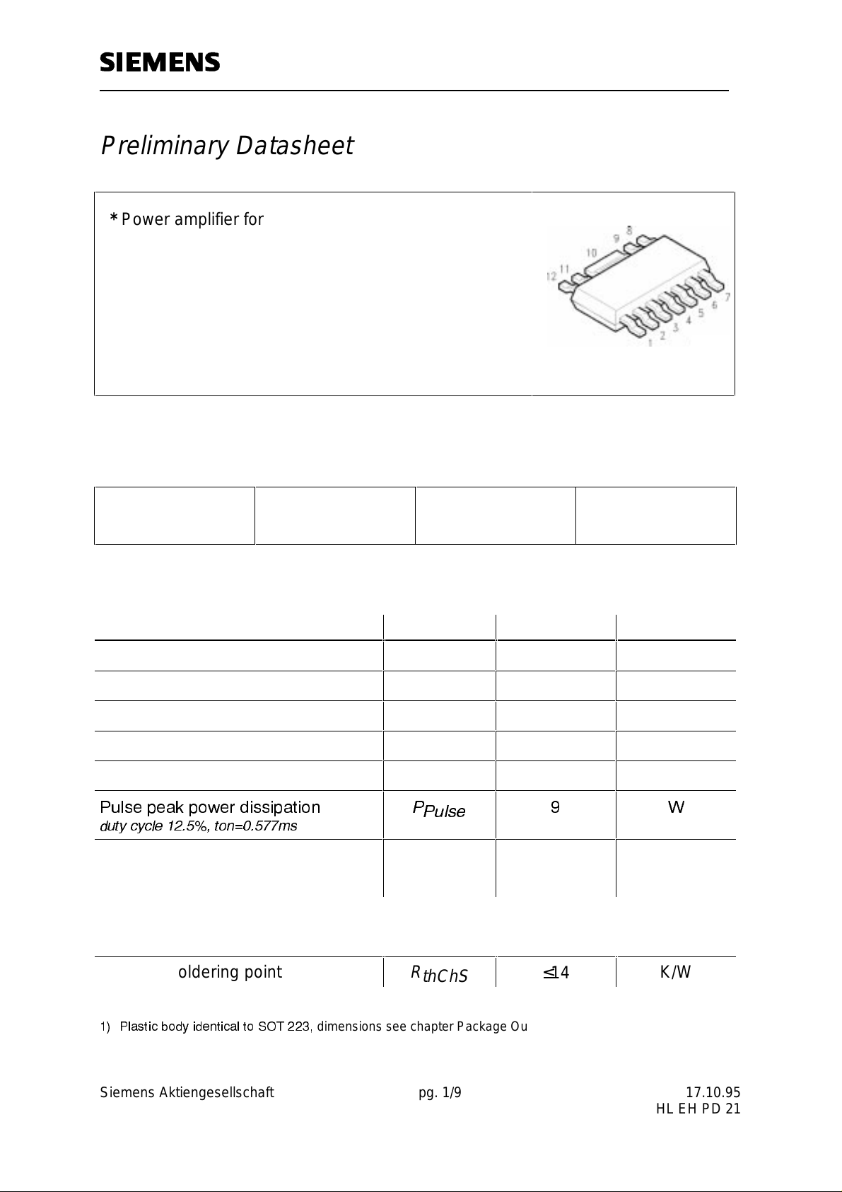
* Power amplifier for GSM or AMPS application
* Fully integrated 2 stage amplifier
* Operating voltage range: 2.7 to 6 V
* 2 W output power at 3.6 V
* Overall power added efficiency 46 %
* Input matched to 50 Ω, simple output match
ESD: Electrostatic discharge sensitive device,
observe handling precautions!
Type Marking Ordering code
(taped)
Package 1)
CGY 94 CGY 94 Q68000-A9124 MW 12
Maximum ratings
Characteristics Symbol max. Value Unit
Positive supply voltage V
Negative supply voltage 2)V
Supply current
Channel temperature
Storage temperature
Pulse peak power dissipation
duty cycle 12.5%, ton=0.577ms
Total power dissipation
Ts: Temperature at soldering point
(Ts ≤ 81 °C)
D
G
I
D
T
Ch
T
stg
P
Pulse
P
tot
9V
-8 V
2A
150 °C
-55...+150 °C
9W
5W
Thermal Resistance
Channel-soldering point
1) Plastic body identical to SOT 223,
= -8V only in combination with V
2) V
G
Siemens Aktiengesellschaft pg. 1/9 17.10.95
HL EH PD 21
dimensions see chapter Package Outlines
= 0V; VG = -6V while V
TR
R
thChS
TR
≠ 0V
≤14
K/W
Page 2
GaAs MMIC CGY 94
_______________________________________________________________________________________________________
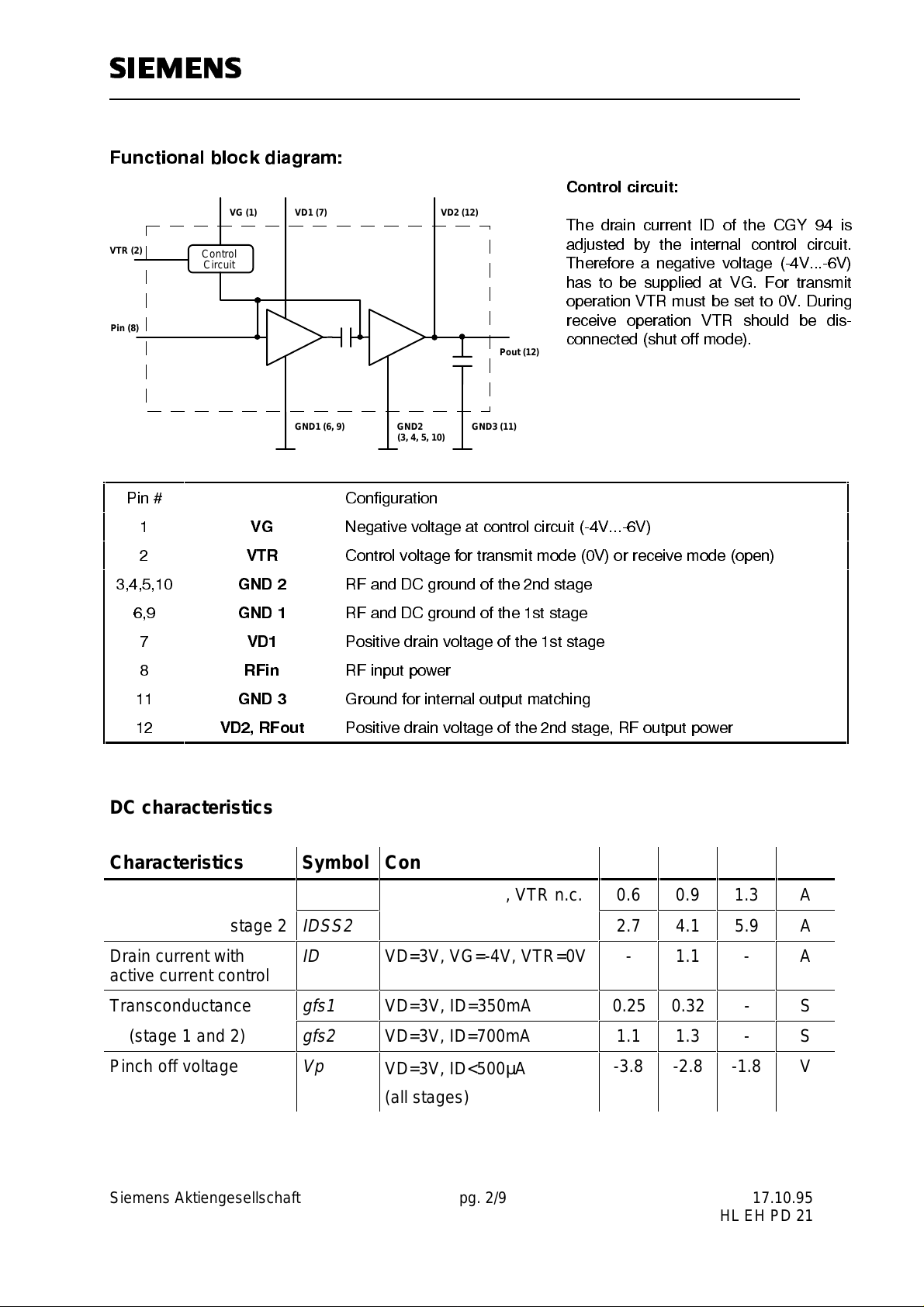
Functional block diagram:
Control circuit:
VTR (2)
Pin (8)
Control
Circuit
VD1 (7) VD2 (12)VG (1)
Pout (12)
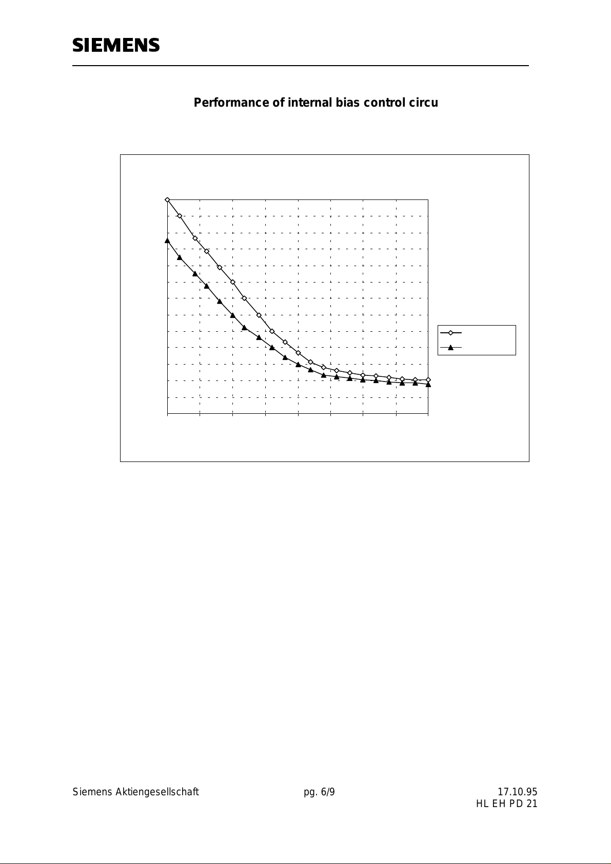
The drain current ID of the CGY 94 is
adjusted by the internal control circuit.
Therefore a negative voltage (-4V...-6V)
has to be supplied at VG. For transmit
operation VTR must be set to 0V. During
receive operation VTR should be dis-
connected (shut off mode).
GND1 (6, 9) GND2
(3, 4, 5, 10)
GND3 (11)
Pin # Configuration
1
2
3,4,5,10
6,9
7
8
11
12
VG
VTR
GND 2
GND 1
VD1
RFin
GND 3
VD2, RFout
Negative voltage at control circuit (-4V...-6V)
Control voltage for transmit mode (0V) or receive mode (open)
RF and DC ground of the 2nd stage
RF and DC ground of the 1st stage
Positive drain voltage of the 1st stage
RF input power
Ground for internal output matching
Positive drain voltage of the 2nd stage, RF output power
DC characteristics
Characteristics Symbol Conditions min typ max Unit
Drain current stage 1
stage 2
Drain current with
IDSS1
IDSS2
ID
VD=3V, VG=0V, VTR n.c. 0.6 0.9 1.3 A
2.7 4.1 5.9 A
VD=3V, VG=-4V, VTR=0V - 1.1 - A
active current control
Transconductance
(stage 1 and 2)
Pinch off voltage
gfs1
gfs2
Vp
VD=3V, ID=350mA 0.25 0.32 - S
VD=3V, ID=700mA 1.1 1.3 - S
VD=3V, ID<500µA
-3.8 -2.8 -1.8 V
(all stages)
Siemens Aktiengesellschaft pg. 2/9 17.10.95
HL EH PD 21
Page 3
GaAs MMIC CGY 94
_______________________________________________________________________________________________________
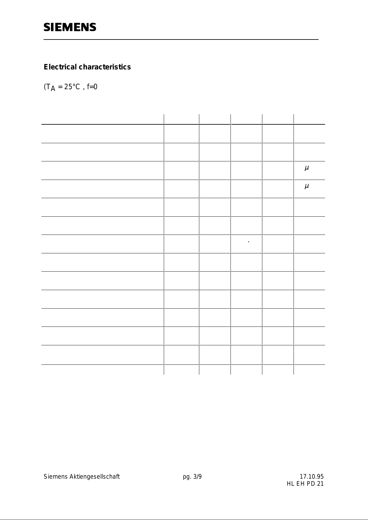
Electrical characteristics
(TA = 25°C , f=0.9 GHz, ZS=ZL=50 Ohm, VD=3.6V, VG=-4V, VTR pin connected to
ground, unless otherwise specified; pulsed with a duty cycle of 10%, ton=0.33ms)
Characteristics Symbol min typ max Unit
Supply current
VD=3.0V; Pin=10dBm
Negative supply current
(normal operation)
Shut-off current
VTR n.c.
Negative supply current
(shut off mode, VTR pin n.c.)
Gain
Pin=-5dBm
Power gain
VD=3.6V; Pin=10dBm
Output Power
VD=3.0V; Pin=10dBm
Output Power
VD=3.6V; Pin=10dBm
Output Power
VD=5V; Pin=10dBm
Overall Power added Efficiency
VD=3.0V; Pin=10dBm
Overall Power added Efficiency
VD=3.6V; Pin=10dBm
Overall Power added Efficiency
VD=5V; Pin=10dBm
Harmonics
VD=3.6V; (P
Input VSWR
(Pin=10dBm, CW)
=33.1dBm)
out
VD=3.6V;
3f
2f
I
DD
I
G
I
D
I
G
G
G
P
o
P
o
P
o
η
η
η
0
0
-
-
- 1.18 - A
-2-mA
- 400 -
-10-
µ
A
µ
A
27.0 29.0 - dB
22.8 23.6 - dB
31.5 32.3 - dBm
32.8 33.6 - dBm
34.5 35.5 - dBm
43 48 - %
42 47 - %
41 46 - %
-
-
-49
-45
-
-
dBc
dBc
- - 1.5 : 1 2.0 : 1 -
Siemens Aktiengesellschaft pg. 3/9 17.10.95
HL EH PD 21
Page 4
GaAs MMIC CGY 94
AAAA
AAA
AAAAA
AAA
A
A
AAAA
A
_______________________________________________________________________________________________________
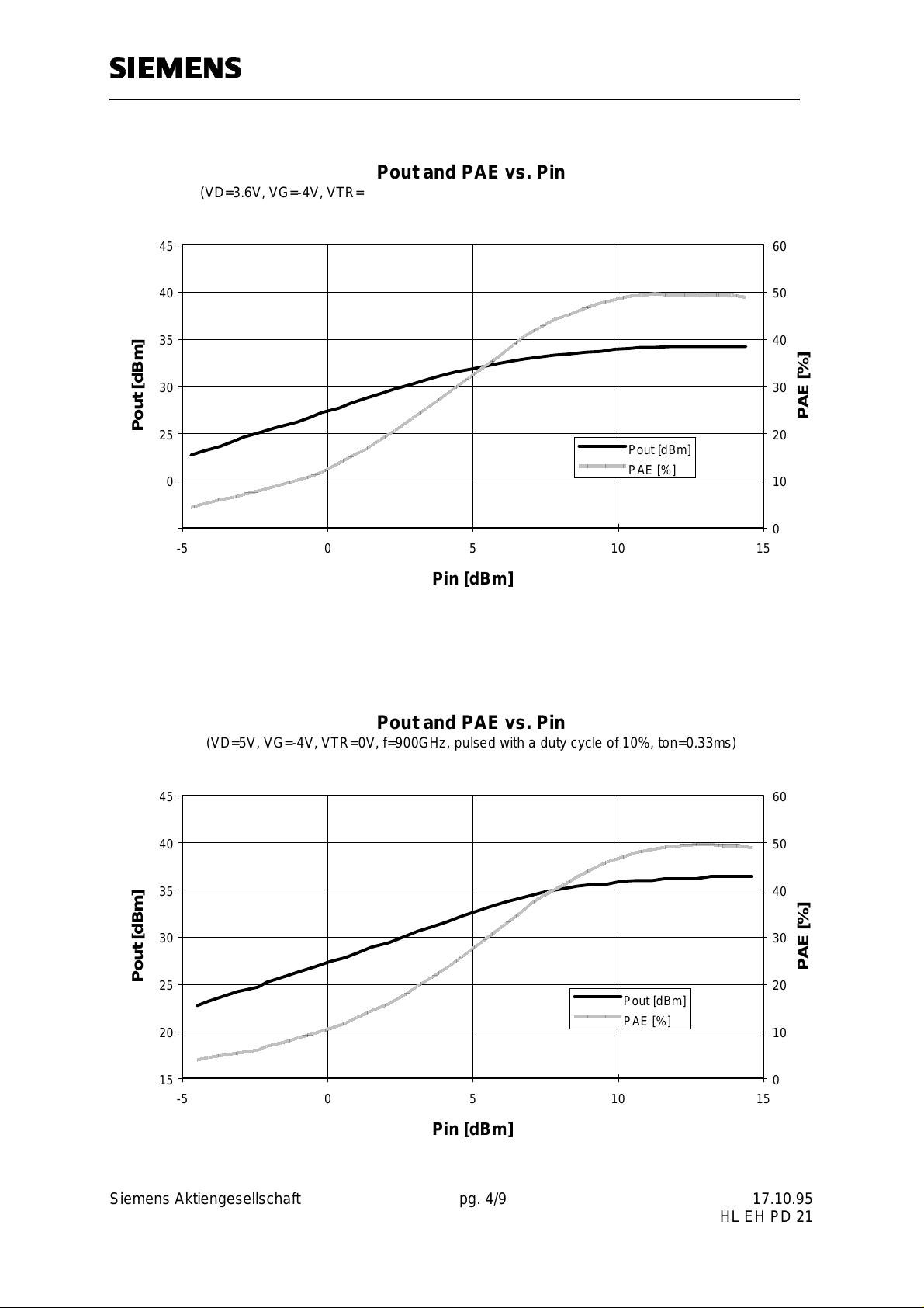
Pout and PAE vs. Pin
(VD=3.6V, VG=-4V, VTR=0V, f=900GH z, pulsed with a duty cycle of 10%, ton=0.33ms)
45
40
35
30
Pout [dBm]
25
Pout [dBm]
20
PAE [%]
15
-5 0 5 10 15
Pin [dBm]
60
50
40
30
PAE [%]
20
10
0
Pout and PAE vs. Pin
(VD=5V, VG=-4V, VTR=0V, f=900GHz, pulsed with a duty cycle of 10%, ton=0.33ms)
45
40
35
30
Pout [dBm]
25
20
15
-5 0 5 10 15
Pin [dBm]
Pout [dBm]
PAE [%]
60
50
40
30
PAE [%]
20
10
0
Siemens Aktiengesellschaft pg. 4/9 17.10.95
HL EH PD 21
Page 5
GaAs MMIC CGY 94
_______________________________________________________________________________________________________
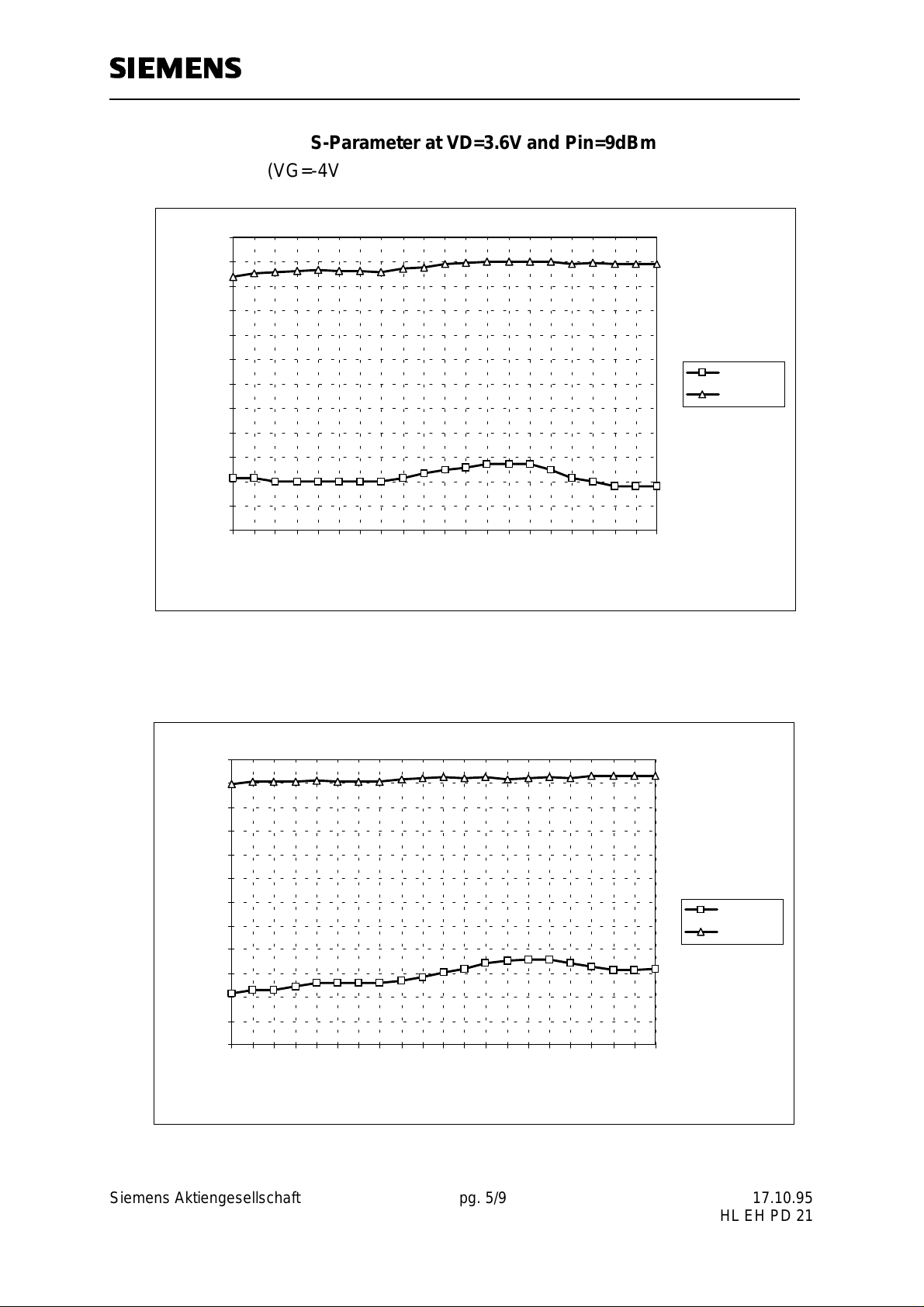
S-Parameter at VD=3.6V and Pin=9dBm
(VG=-4V, VTR=0V, pulsed with a duty cycle of 10%)
30
25
20
15
10
5
0
Mag [dB]
-5
-10
-15
-20
-25
-30
MAG(s11)
MAG(s21)
30
25
20
15
10
5
0
Mag [dB]
-5
-10
-15
-20
-25
-30
750
770
790
810
830
850
870
890
910
930
f [MH z ]
S-Parameter at VD=5V and Pin=9dBm
(VG=-4V, VTR=0V, pulsed with a duty cycle of 10%)
950
MAG(s11)
MAG(s21)
750
770
790
810
830
850
870
890
910
930
950
f [MH z ]
Siemens Aktiengesellschaft pg. 5/9 17.10.95
HL EH PD 21
Page 6
GaAs MMIC CGY 94
_______________________________________________________________________________________________________
Performance of internal bias control circuit
(VTR=0V)
3,0
2,8
2,6
2,4
2,2
2,0
1,8
ID / A
1,6
1,4
1,2
1,0
0,8
0,6
0,4
2,0 2,5 3,0 3,5 4,0 4,5 5,0 5,5 6,0
ID (V D=3.0V )
ID (V D=6.0V )
-Vg / V
Siemens Aktiengesellschaft pg. 6/9 17.10.95
HL EH PD 21
Page 7
GaAs MMIC CGY 94
_______________________________________________________________________________________________________
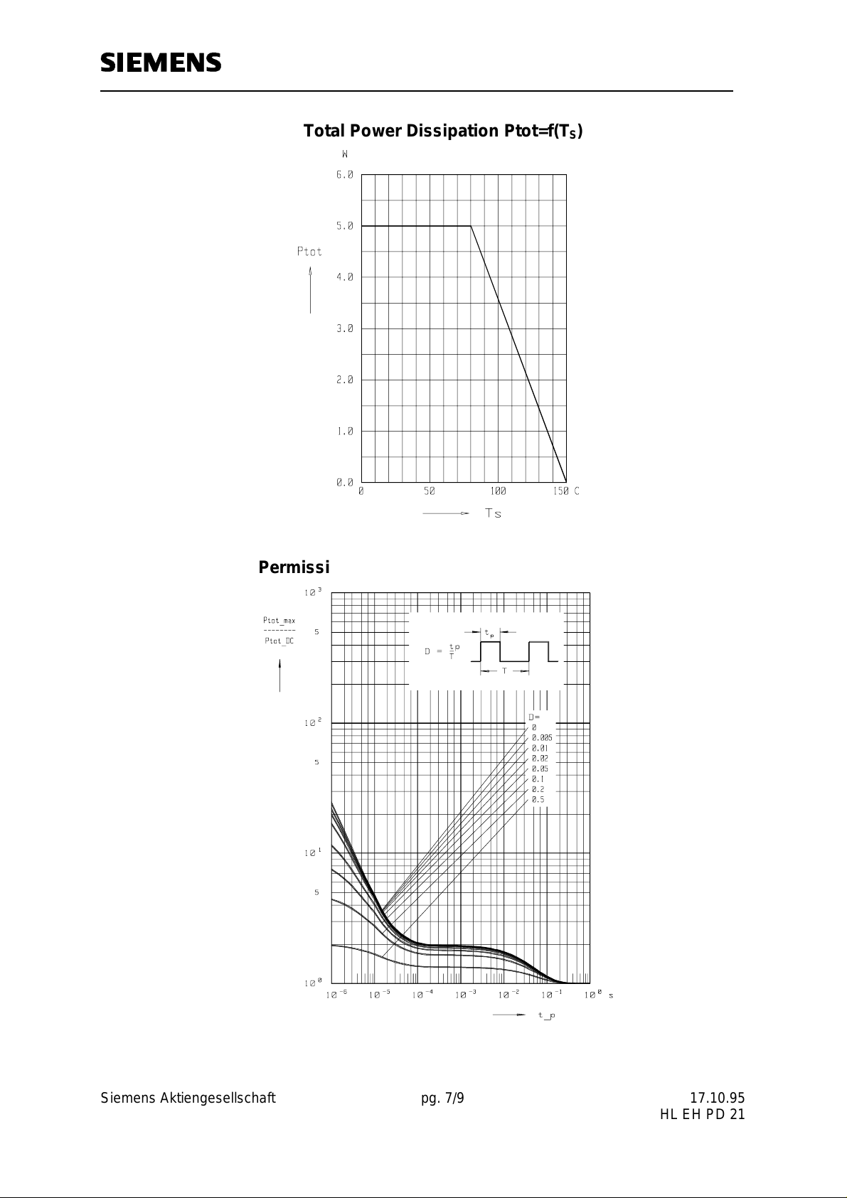
Total Power Dissipation Ptot=f(TS)
Permissible pulse load P
tot_max/Ptot_DC
= f(t_p)
Siemens Aktiengesellschaft pg. 7/9 17.10.95
HL EH PD 21
Page 8
GaAs MMIC CGY 94
G
_______________________________________________________________________________________________________
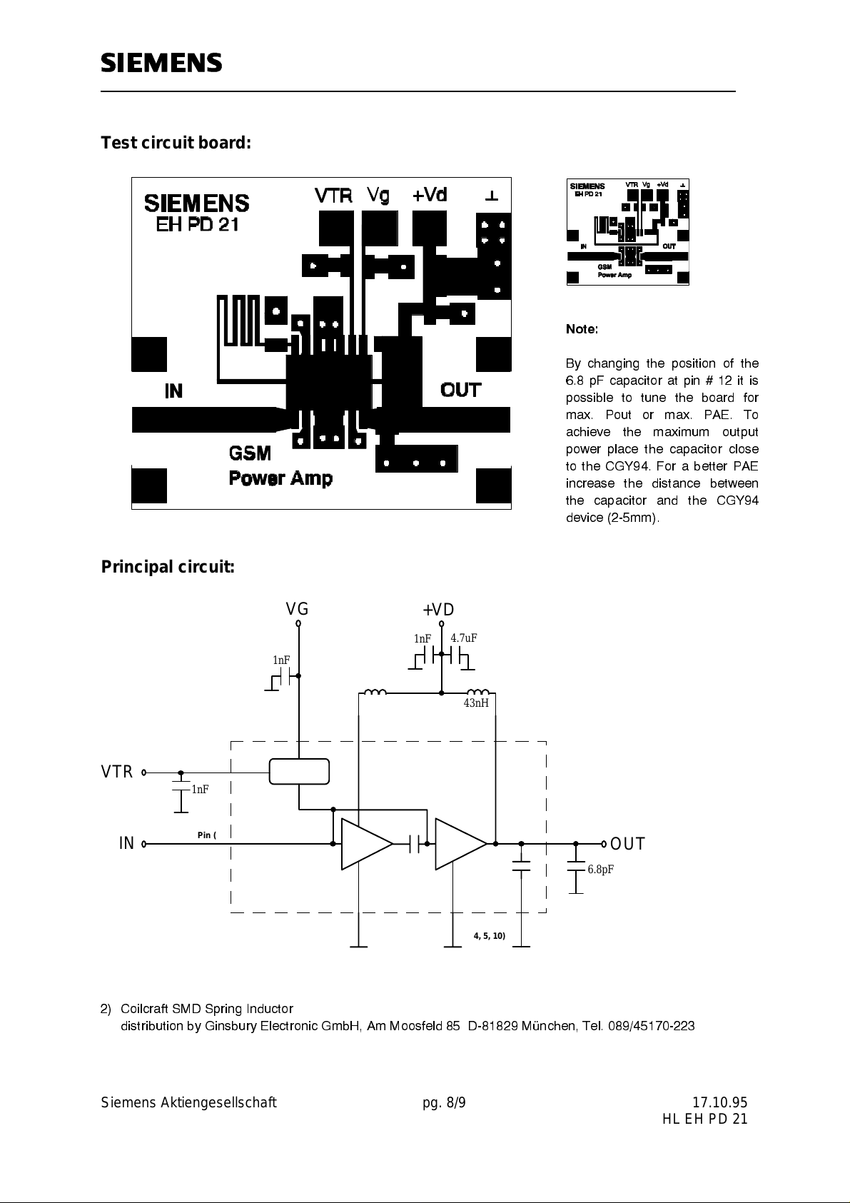
Test circuit board:
Note:
By changing the position of the
43nH
6.8 pF capacitor at pin # 12 it is
possible to tune the board for
max. Pout or max. PAE. To
achieve the maximum output
power place the capacitor close
to the CGY94. For a better PAE
increase the distance between
the capacitor and the CGY94
device (2-5mm).
Principal circuit:
VTR (2)
VTR
1nF
IN
Pin (8)
1nF
Control
Circuit
V
+VD
4.7uF
1nF
43nH
VD1 (7) VD2 (12)VG (1)
GND1 (6, 9) GND2
(3, 4, 5, 10)
Pout (12)
OUT
6.8pF
GND3 (11)
2) Coilcraft SMD Spring Inductor
distribution by Ginsbury Electronic GmbH, Am Moosfeld 85 D-81829 München, Tel. 089/45170-223
Siemens Aktiengesellschaft pg. 8/9 17.10.95
HL EH PD 21
Page 9

GaAs MMIC CGY 94
_______________________________________________________________________________________________________
APPLICATION - HINTS
1. CW - capability of the CGY94
Proving the possibility of CW - operation there must be known the total power dissipation of the
device. This value can be found as a function of the temperature in the datasheet (page 7). The
CGY94 has a maximum total power dissipation of P
As an example we take the operating point with a drain voltage VD = 3 V and a typical drain current
of ID=1.0 A. So the maximum DC - power can be calculated to:
PVI W
=⋅=3
DC D D
This value is smaller than 5 W and CW - operation is possible.
By decoupling RF power out of the CGY94 the power dissipation of the device can be further
reduced. Assuming a power added efficiency (PAE) of 40 % the total power dissipation P
calculated using the following formula:
P P PAE W W
=−=−=()(.).13104018
tot DC
2. Operation without using the internal current control
If you don' t want to use the internal current control, it is recommended to connect the negative
= 5 W.
tot
tot
can be
supply voltage at pin 1 (VTR) instead of pin 2 (VG). In that case VG is not connected.
3. Biasing and use considerations
Biasing should be timed in such a way, that the gate voltage (VG) is always applied before the drain
voltage (VD), and when returning t o the standby mode, the drain voltage has t o be removed before
the gate voltage.
Siemens Aktiengesellschaft pg. 9/9 17.10.95
HL EH PD 21
 Loading...