

Page 1

CGY 21
GaAs MMIC CGY 21
● Two-stage monolithic microwave IC (MMIC amplifier)
● All gold metallization
● Chip fully passivated
● Operating voltage range: 3 to 6 V
● 50 Ω input/output; RLIN RLOUT > 10 dB
● Gain: 21 dB at 500 MHz
● Low noise figure: 3.9 dB at 500 MHz
● Bandwidth: 2 GHz
● Hermetically sealed package
ESD: Electrostatic discharge sensitive device, observe handling precautions!
Type Ordering Code
Circuit Diagram (Pin Configuration)
Package
CGY 21 Q68000-A5953 TO-12
1 RF output,
2 Interstage,
3 RF input
4 RF and DC
ground, case
V
S
V
S
1)
1)
For detailed information see chapter Package Outlines.
Semiconductor Group 1
Page 2

CGY 21
Maximum Ratings
Parameter Symbol Values Unit
Supply voltage, T
Total power dissipation, T
C ≤ 80 ˚C VS 6V
C ≤ 50 ˚C Ptot 2W
Channel temperature Tch 150 ˚C
Storage temperature range T
stg – 55 … + 150
Thermal Resistance
Channel - case RthchC 50 K/W
Note: Exceeding any of the maximum ratings may cause permanent damage to the device.
Appropriate handling procedures are required to protect the electrostatic sensitive IC
against degradation due to excess voltage or excess current spikes. Excellent ground
connection of lead 4 and the package (e. g. soldered on microstripline laminate) is
required to achieve guaranteed RF performance and stable operation conditions and
provides adequate heat sink. Low parasitic capacitance of the bias network to port 2
gives optimum gain and flatness. Input and output connections must be DC isolated by
coupling capacitors.
Semiconductor Group 2
Page 3

Electrical Characteristics
A = 25 ˚C, VS = 4.5 V, RS = RL = 50 Ω, unless otherwise specified,
at T
(for application circuit see next page).
CGY 21
Parameter Symbol
G 19 21 –
f= 100 MHz to 900 MHz
Gain flatness
∆G – 1.5 2
f= 100 MHz to 900 MHz
Noise figure
F – 3.9 5.5
f= 100 MHz to 900 MHz
Input return loss
RLIN – 12 9.5
f= 100 MHz to 900 MHz
Output return loss
RLOUT – 12 9.5
f= 100 MHz to 900 MHz
IP3 31 32.5 –
two-tone intermodulation test
1= 806 MHz, f2= 810 MHz,
f
o = 10 dBm (both carriers)
P
UnitValues
min. typ. max.
mAOperating current Iop – 160 200
dBPower gain
dBmThird order intercept point
1 dB gain compression
f= 100 MHz to 900 MHz
P1dB –19–
Semiconductor Group 3
Page 4

Application Circuit
L
f= 100 MHz to 900 MHz
CGY 21
Legend of components
C1, C2, C3 1 nF chip capacitors
1, L2 1 µH inductance (B 78108 - T 1102K)
D 6 V2 Zener diode (BZW 22C6V2)
Semiconductor Group 4
Page 5
CGY 21
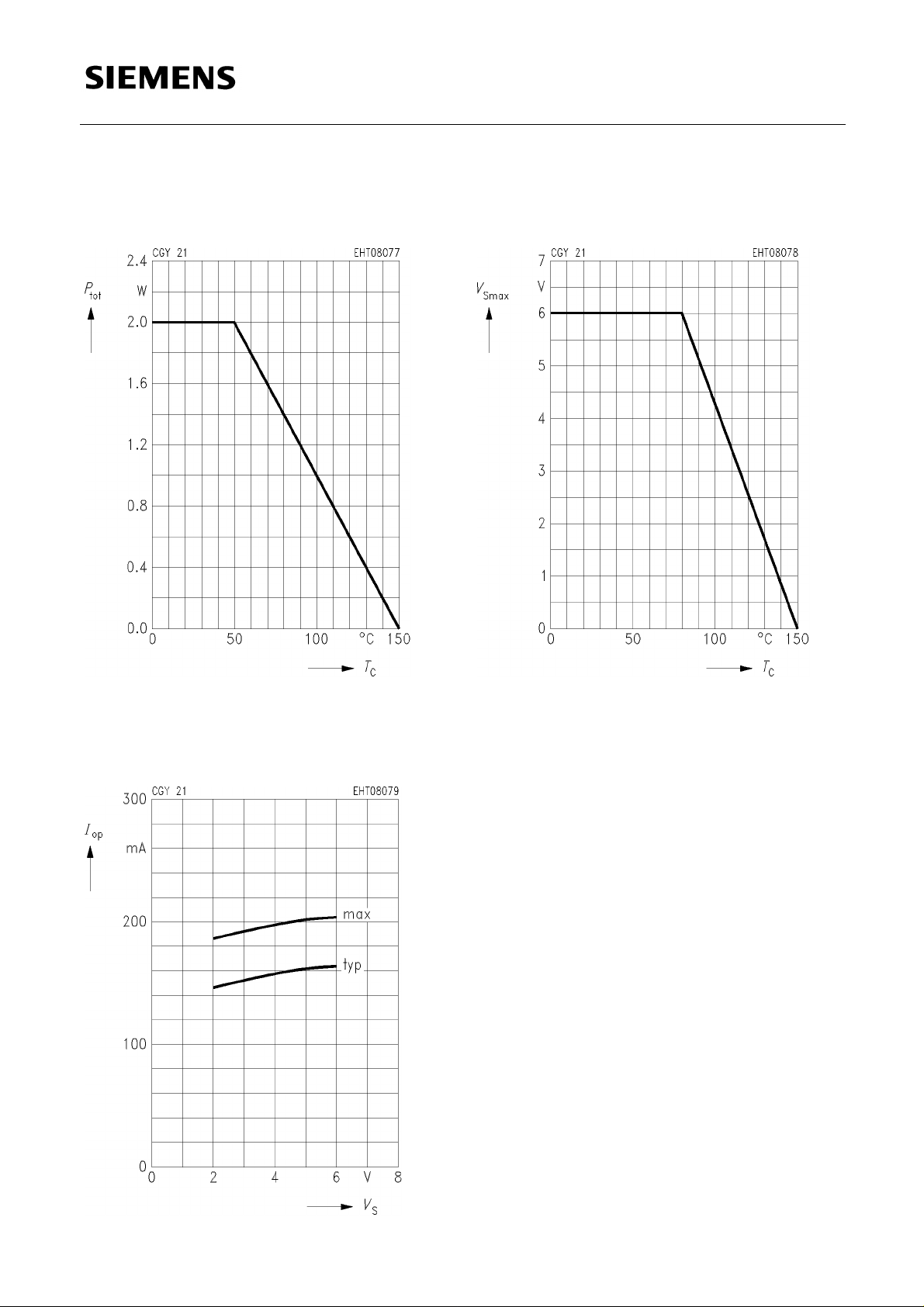
Total power dissipation Ptot = f (TC)
Max. supply voltage VSmax = f (TC)
Operating current I
op = f (VS)
Semiconductor Group 5
Page 6
CGY 21
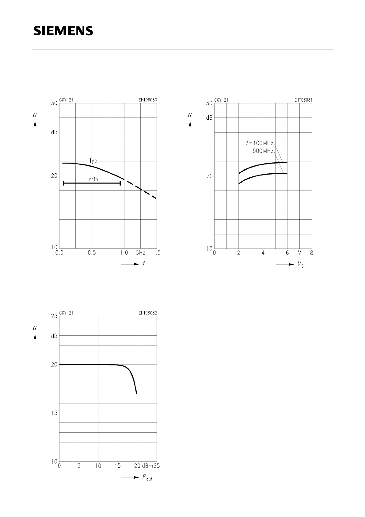
Power gain G = f (f)
S = 4.5 V, RS = RL = 50 Ω
V
Power gain G = f (VS)
S = RL = 50 Ω
R
Power gain G = f (Pout)
S = 4.5 V, RS = RL = 50 Ω
V
f= 0.8 GHz
Semiconductor Group 6
Page 7
CGY 21
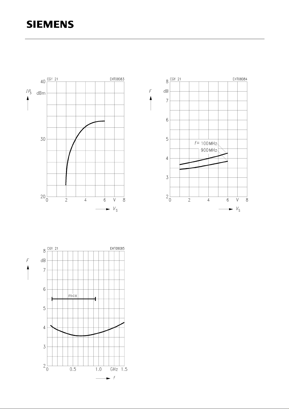
Third order intercept point IP3 = f (VS)
f= 800 MHz, R
S = RL = 50 Ω
Noise figure F = f (VS)
S = RL = 50 Ω
R
Noise figure F = f (f)
S = 4.5 V, RS = RL = 50 Ω
V
Semiconductor Group 7
Page 8

CGY 21
S Parameters
fS11 S21 S12 S22
GHz MAG ANG MAG ANG MAG ANG MAG ANG
VS = 4.5 V, Z0 = 50 Ω
0.1
0.3
0.5
0.7
0.9
1.1
1.3
1.5
0.02
0.08
0.14
0.18
0.23
0.27
0.28
0.25
S11 = f (f)
S = 4.5 V, Z0 = 50 Ω
V
49
55
34
17
– 15
– 28
– 39
13.82
13.63
13.03
12.1
0
10.93
9.48
7.91
6.29
– 10
– 34
– 58
– 81
– 104
– 127
– 149
– 171
0.012
0.012
0.012
0.011
0.011
0.01
0.009
0.008
– 2
– 7
– 13
– 19
– 24
– 29
– 31
– 32
0.11
0.13
0.15
0.19
0.24
0.29
0.33
0.36
3
11
18
20
20
16
12
5
S12 = f (f)
S = 4.5 V, Z0 = 50 Ω
V
Semiconductor Group 8
Page 9
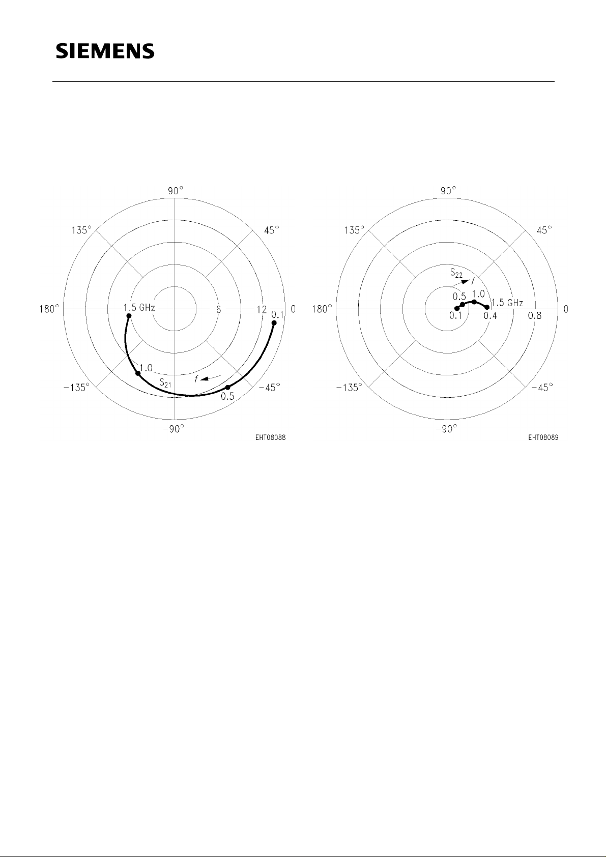
S Parameters (continued)
CGY 21
21 = f (f)
S
S = 4.5 V, Z0 = 50 Ω
V
S22 = f (f)
S = 4.5 V, Z0 = 50 Ω
V
Semiconductor Group 9
 Loading...