

Page 1
CH1782A
Family of Ultra Small Modem Modules V.22bis-2400bps
INTRODUCTION FEATURES
The CH1782A Ultra Small Modem Module is a pin
compatible and functional replacement for the
CH1782. The CH1782A replaces the CH1782 due to
the obsolescence of the modem chip set in the
CH1782 by the manufacturer. The CH1782A is
recommended as a replacement for the CH1782, but
not for new designs. The CH1782A is a small, full
function 2400bps modem component that is FCC Part
68 approved. It offers a fast and easy way to integrate
a modem into an OEM product while utilizing a
minimum amount of PCB space and having only an
0.50” height. The modem component has two
interfaces, a CCITT V.24 serial interface that can be
routed directly to a UART and a Tip and Ring signal
which goes directly to an RJ-11 jack for telephone line
connection. The modem can be controlled with
industry standard AT commands and, hence, is
compatible with available industry communication
software.
• Supports Standards CCITT V.22bis, V.22, Bell
212, and Bell 103
• FCC Part 68 approved and DOC approvable
• AT Command structure – with extensions
• 1000 VAC isolation barrier
• Single 5 volt operation
• Low power operation with automatic reduced
power standby mode
• Automatic adaptive and fixed compromise
equalization
• Size: 1.0”X1.25”X0.53”
The CH1782A supports asynchronous operations at
2400bps, 1200bps, and 300bps to Bell and CCITT
standards.
The resident telephone line interface, or Data Access
Arrangement (DAA), while being FCC approved, is
also Canadian DOC approvable and can be approved
in other countries that require 1000 VAC isolation.
The CH1782A operates off a regulated single 5-volt
supply. The low power operation and automatic
standby mode male it ideal for portable equipment,
which is further enhanced by its small size.
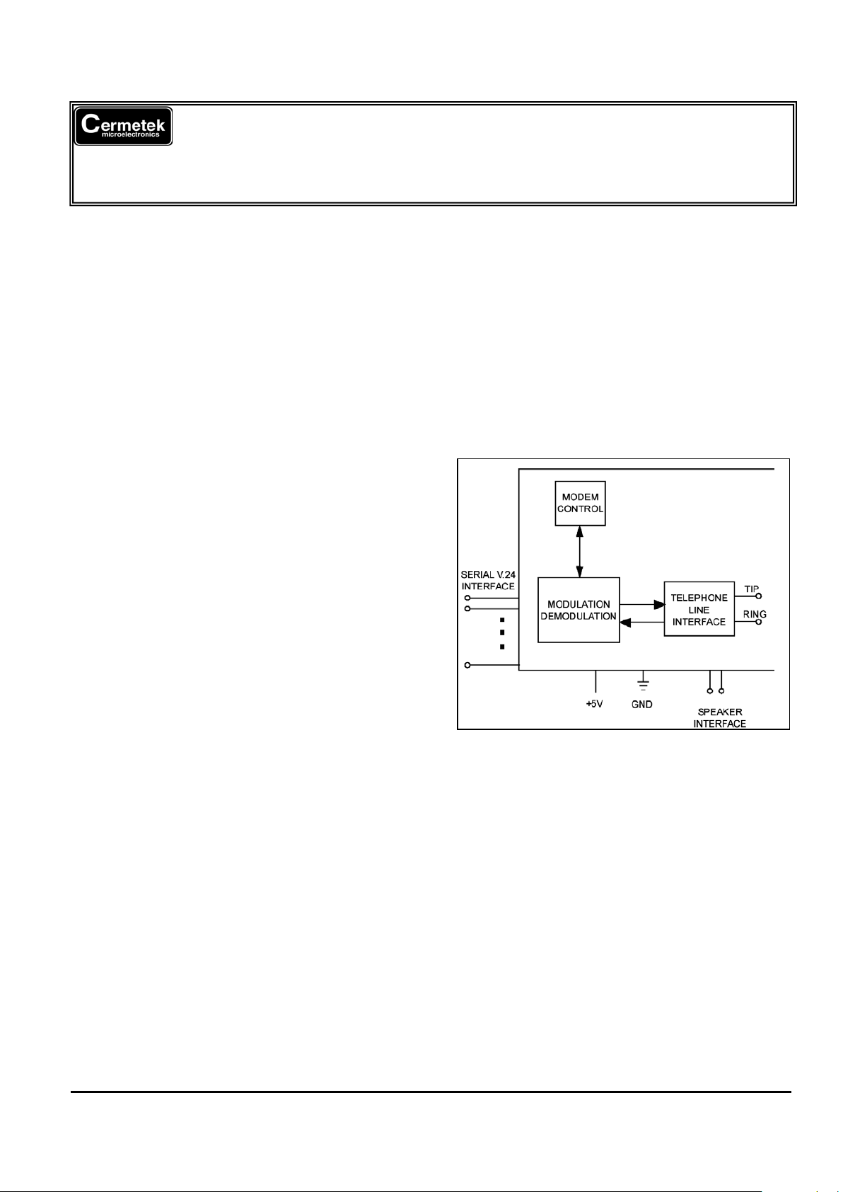
Figure 1. CH1782A Functional Block Diagram.
Telephone Line Interface or DAA. The CH1782A is
designed to meet North American telephone standards
as set by FCC Part 68 and DOC. The telephone line
interface is designed to meet 1000 VAC and 1500 volt
peak surge isolation, among other parameters. As
such, it will meet U.S. and Canadian requirements, as
well as other international requirements that specify
that level of isolation. Cermetek manufacturers other
modules that meet more stringent international
requirements.
DESCRIPTION OF FUNCTIONAL BLOCKS
AND DISCUSSION OF BASIC OPERATIONS
Figure 1 is a functional block drawing of the CH1782A.
The CH1782A is a highly integrated, full-function
modem, comprised of a modulator/demodulator,
controller, and a FCC Part 68 approved telephone
PSTN line interface.
Modulation/Demodulation and Modem Controller.
These functions are provided by a monolithic modem
integrated circuit. This IC has built-in facilities to
accommodate integrated AT command control and
contains the necessary resident interfaces for general
communication and routing to the DAA.
The CH1782A is pre-approved to FCC Part 68; and is
shipped from the factory with a label that indicates the
registration number and ringer equivalent affixed to the
unit. An additional label is provided that should be
prominently displayed on the outer system enclosure.
As with most countries, except the U.S., Canada
requires submission of the product containing the
CH1782A for DOC approval. This can be done by
2002 Cermetek Microelectronics, Inc. Page 1 Document No. 607-0009 Revision C (01/03)
Page 2
Cermetek Microelectronics, Inc. CH1782A Family of Ultra Small Modem Modules V.22bis-2400bps
submitting the design to a test house or consultant.
Call Cermetek for assistance.
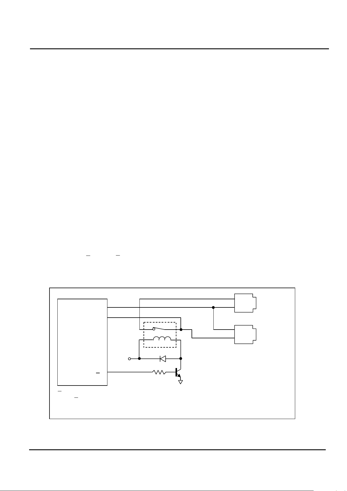
to activate a relay which can switch a telephone on or
off the Tip and Ring incoming PSTN lines. This
feature allows any telephone associated with the
CH1782A to be disconnected when a data call is in
progress, thereby preventing the data from being
disturbed by an inadvertent telephone pick-up. See
Figure 2.
SUPPORT FEATURES
AT Command Set. A 40-character command line is
supported. The command line starts with AT and
may contain standard or enhanced commands. The
commands are compatible with EIA Document
TR302.2/88-08006.
Speed and Parity Selection. Prior to call initiation,
the host controller trains the modem to the host
speed (2400,1200 or 300bps) and parity (odd, even,
mark, space, or none) via a host-initiated training
sequence. This training also sets the speed of the
data for originate calls. The CH1782A will
automatically adjust to the originator’s speed when
answering calls.
Serial Host Interface. The serial interface is a V.24
(EIA-232) compatible interface. Ten Bits total: 1 start
bit, 1 stop bit, and eight data bits which can be either
eight bits with no parity or seven odd or even with
parity. The start bit is LOW going. RXD and TXD
data is non-inverted. See pin description in Table 2.
The CH1782A matches the host’s parity when it
returns status messages to the host. During a data
connection, however, the modem passes parity
through without interpretation or alteration.
Speaker Interface. The SPK output reflects the
receiver analog input and provides a signal that can
be used to monitor call progress. The SPK signal can
drive a 300 Ω load directly. Typically, the SPK signal
is input into an audio power amplifier and the
amplifier, in turn, drives the speaker coil. The
speaker is activated with the ATMn command. The
speaker volume is adjusted using the ATLn
command, where n is 0,1,2,or 3. Increasing numbers
correspond to higher volume. Figure 5 indicates one
method of driving an external 8 Ω speaker.
Sleep Mode. To minimize power consumption, the
CH1782A includes a power down feature called
Sleep Mode. When activated, the CH1782A will
automatically enter Sleep Mode after 0 to 254
seconds of inactivity. The inactivity delay is selected
using the ATS24 command. The CH1782A is
delivered from the factory with a 5 second inactivity
delay enabled (i.e., ATS24=5). The CH1782A
returns to normal operation when a ring signal is
received or upon an input low signal on the TXD pin.
ATS24=255 disables the Sleep Mode and is the
default if no value is set in register S24.
Phone Control. Cermetek ’s CH1782A contains a pin
called Voice or Data (V/D). The V/D pin toggles high
when the modem goes off hook. This pin can be used
V/D pin is used to create a separate port for telephone connection sharing of the tip and ring
lines. V/D is TTL compatible (IOL = 1.6mA, VOL = 0.4V) and is active during data connection
thereby isolating the telephone from the tip and ring lines. (Note: the relay chosen must meet
the appropriate regulatory agency requirements).
V/D
TELEPHONE
LINE
OPTIONAL
PHONE
RJ-11
Jack
RJ-11
Jack
TIP
TIP
RING
RING
+5V
IN914
10K
1
2
12
CH1782A
Figure 2. Use of V/D pin to ensure that a shared PSTN line does not inadvertently disturb
an active data call.
2002 Cermetek Microelectronics, Inc. Page 2 Document No. 607-0009 Revision C (01/03)
Page 3

Cermetek Microelectronics, Inc. CH1782A Family of Ultra Small Modem Modules V.22bis-2400bps
A SLEEP output signal is available to control power to
external devices. In Figure 6, a FET controlled by the
SLEEP signal turns of the external speaker amplifier
when the CH1782A enters Sleep Mode. In Sleep
Mode, power is reduced to approximately 50% of
normal operating power.
NOTE
A 2400-baud connection rate will only result if both
modems are initially set at 2400 baud.
Table 1. Connection Rates.
Answering
Modem Initial
Trained Rate
Connection Rate Resulting
When Calling Modem Initial
Rate Is:
300 1200 2400
300 300 1200 1200
1200 300 1200 1200
2400 300 1200 2400
Guard Tone. A guard tone of 550 Hz or 1800 Hz can
be generated at 6 dB or 9 dB below the transmit level,
respectively, by using the &Gn command. Refer to
“Cermetek AT Commands and S-Registers reference
Guide” or the Cermetek web site at
http://www.cermetek.com
.
Ring Indicator (RI). The RI pin follows the frequency
of the ring signal and toggles low when the CH1782A
detects an incoming call. The ring signal is typically
20 to 30 Hz and is on for 2 seconds and off for 4
seconds. Although not TTL compliant, the RI pin can,
nonetheless, be utilized to activate external circuitry
including the external RST pin.
Answer Tone. A CCITT (2100 Hz) or Bell (2225Hz)
answer tone is generated depending on the selected
configuration. Refer to “Cermetek AT commands and
S-Registers Reference Guide” or the Cermetek web
site at http://www.cermetek.com
.
Data Encoding. The data encoding conforms to
CCITT recommendations V.22bis or V.22, or
Bell212A, or 103, depending on the selected
configuration. Refer to “Cermetek AT commands and
S-Register Reference Guide” or the Cermetek web
site at http://www.cermetek.com
.
When using the RI pin, it is recommended that a
Schmitt Trigger or the Isolated Envelope Detect
Circuit in Figures 3 or 5 be placed between the RI pin
and the external load.
Power Supply. The CH1782A modem module is a
complex set of sub-systems. During the course of
normal operation the CH1782A decodes analog
signals from the telephone line that are in the millivolt
range. Steps must be taken by the user to guarantee
that power supply noise on all supply lines, including
ground, does not exceed 50 mV peak to peak. Any
frequency between 20 kHz and 150 kHz must be less
than 500 micro volts peak. If necessary, use
dedicated power and ground planes. Failure to
provide such operating conditions could cause the
CH1782A to malfunction or to function erratically.
Line Equalization. Transmitter and receiver digital
filters compensate for delay and amplitude distortion
during operation on nominal phone lines. In addition,
automatic adaptive equalization in the receiver
minimizes the effects of inter symbol interference.
Transmission Speed. In normal operation, the
originating modem initiates the call and attempts to
connect to the answering modem at a speed
established by the originating modem’s controller prior
to call initiation. This is referred to as the Initial
Trained Rate. Upon receiving the call, the answering
modem will attempt to connect to the originating
modem at its Initial Trained Rate. If these two rates
are identical, the connection is made. If the speeds
differ, the answering modem must adjust its rate or
terminate the call. Table 1 indicates the connection
rate that will result when the calling modem’s Initial
Trained Rate and the answering modem’s Initial
Trained Rate are different.
The CH1782A requires a single +5V ±5% supply. It
is recommended that by-pass capacitors be placed
on the power supply as close to the modem’s supply
input as practical. It’s recommended a 10 µF
Tantalum capacitor in parallel with a 0.01 µF ceramic
capacitor be used.
INITIALIZING THE MODEM
MODEM CONTROL
Before commands may be sent to the CH1782A, the
CH1782A must be initialized. Initialization is a two
step activity consisting of:
The CH1782A modem may be controlled by sending
serial ASCII command sequences. The commands are
sent to the modem serially on TXD. After execution of
the command, the modem returns a serial status
message on RXD, to indicate the completion status of
the command.
1. Hard Reset. This is accomplished by applying a
hardware reset pulse to pin RST or by switching
the power off and then back on.
2002 Cermetek Microelectronics, Inc. Page 3 Document No. 607-0009 Revision C (01/03)
2. Initial modem training. The CH1782A must be
trained to the host’s speed (2400, 1200, 300bps)
and parity (odd, even, mark, space or none).
Page 4

Cermetek Microelectronics, Inc. CH1782A Family of Ultra Small Modem Modules V.22bis-2400bps
[Commands] represents command strings.
These activities are briefly described below.
<CR> represents carriage return (ASCII 13
or HEX 0D).
Reset. Upon applying power to the CH1782A, the
CH1782A automatically generates an internal reset
pulse. The user may also reset the modem externally
by applying a high-going reset pulse to the RST pin
for at least 10ms after the +5V power supply has
stabilized. Delay sending commands to CH1782A for
200ms after reset has been initiated to allow the
CH1782A time to properly reconfigure.
When entering commands to the modem, the
backspace character-control-H (ASCII 8 or HEX 08)
may be used to edit mistakes. AT and A/ may not be
edited. Multiple commands may be placed in the
command line. A command line may be as long as
40 characters, excluding the letters AT. By way of
example, the command below instructs the CH1782A
to configure itself to not echo characters when in
command mode E0 and then put itself in answer
mode A.
Training the Modem. Each modem must be trained
to match its host’s speed and parity so that it is able
to recognize serial asynchronous commands sent to it
by the host’s is UART. The host must retrain the
modem each time a reset pulse is applied on RST or
after a RESET serial command has been issued.
Enter: ATE0A<CR>
Result: OK
Modem Training Command Sequence. The
CH1782A is trained by sending it the following
sequence:
AT Command Set. The available command set is
divided into four types of commands: dial modifiers,
basic commands, ampersand and percent
commands. Refer to the complete list in Table 5.
Enter: AT<CR>
Result: OK
AT Command Data Rate. With the serial interface,
the rate is speed sensed for parity and format.
Where: A and T may be either upper or lower case
but must be the same case.
<CR> represents carriage return
THE STATUS MESSAGES
The AT sequence is referred to as an attention
sequence. The CH1782A will respond with one of the
following status messages, depending on whether it
is optioned for Terse (abbreviated) or Verbose
(English) status messages.
The CH1782A responds with a status message after
each command is executed. This status message
may either be a single digit followed by a carriage
return or a carriage return and line feed with a
message in English, followed by a carriage return and
line feed.
Result: 0<CR> (Terse)
or
n command. Where n=0, 1, 2, 3, 4 establishes the
result codes allowed by the user.
Result: <CR><LF>OK<CR><LF> (Verbose)
Where: <CR> represents carriage return (ASCII 13 or
HEX 0D).
X0: Result Codes 0, 1, 2, 3, 4 allowed
<LF> represents line feed (ASCII 10 or HEX
0A).
X1: Result Codes 0, 1, 2, 3, 4, 5, 10 allowed
X2: Result Codes 0,1, 2, 3, 4, 5, 6, 10 allowed
X3: Result Codes 0, 1, 2, 3, 4, 5, 7, 10 allowed
After responding with an OK, the CH1782A is in idle
mode and is ready to accept additional commands.
An alternate attention sequence A/ may be sent
which behaves much like the AT sequence except
that it causes the previously entered command
specified with an AT prefix to be executed. When
given, both the AT and A/ must be in upper case
ASCII. No carriage return is needed for the A/
command.
X4: Result Codes 0, 1, 2, 3, 4, 5, 6, 7, 10 allowed.
NOTE
The CH1782A is factory set to X4, which allows all
result codes.
MODEM STATES
The CH1782A can be in either command mode or
data mode. When the modem is idle, it is in
command mode by default and will recognize
commands. When data transmission is in progress,
the CH1782A is in the data mode state and will not
recognize commands. To force the CH1782A to
recognize commands, the host must send an escape
sequence to the CH1782A forcing it out of data mode
and into command mode.
THE COMMAND FORMAT
Typical commands consist of three elements: the
attention sequence, the commands themselves, and
a terminating carriage return.
AT[commands]<CR>.
2002 Cermetek Microelectronics, Inc. Page 4 Document No. 607-0009 Revision C (01/03)
Where: AT represents attention sequence.
Page 5
Cermetek Microelectronics, Inc. CH1782A Family of Ultra Small Modem Modules V.22bis-2400bps
Figure 3A. CH1782A Application Diagram indicating the use of Voice/Data pin to control an optional
telephone relay for a secondary telephone.
Table 2. Summary of Result Codes and Meanings.
Result Codes Status Message Meaning
0 OK Command Executed
1 CONNECT Carrier detected at 300bps
2 RING Ring Detected
3 NO CARRIER Did not detect carrier
4 ERROR Entry error
5 CONNECT 1200 Carrier detected at 1200bps
6 NO DIAL TONE Off-hook, but no response after 5 seconds
7 BUSY Busy signal detected
10 CONNECT 2400 Carrier detected at 2400bps
2002 Cermetek Microelectronics, Inc. Page 5 Document No. 607-0009 Revision C (01/03)
Page 6
Cermetek Microelectronics, Inc. CH1782A Family of Ultra Small Modem Modules V.22bis-2400bps
Figure 3B. CH1782A Voice Application illustrating the use of the VI pin to control external injection of voice
or data into the CH1782A and onto the PSTN line.
Table 3. CH1782A Pin Description.
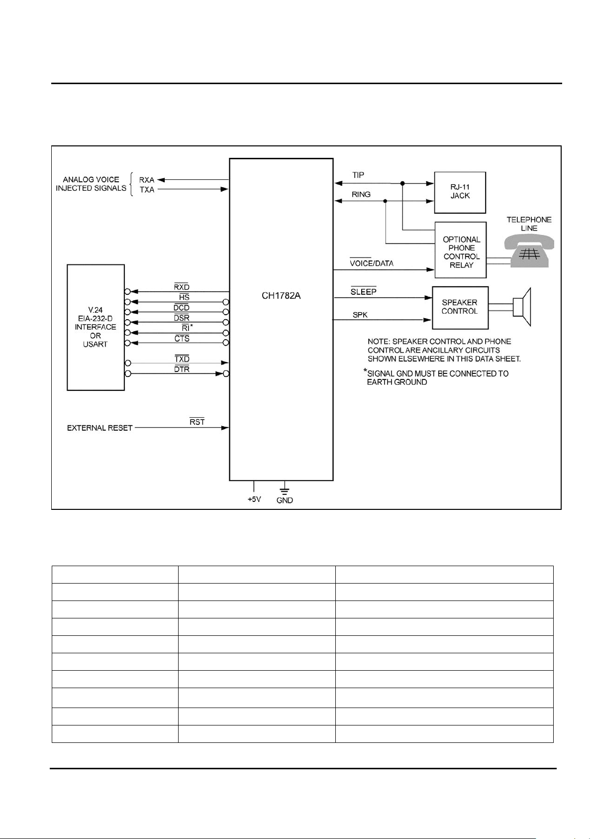
PIN NAME I/O FUNCTION
1 - NC NO CONNECTION. Formerly RTS – Not supported by the CH1782A.
2 GND - GROUND. Note: Noise should be less than 50mV peak to peak.
3 VI I/O VOICE INJECTION. Use this port to transmit/receive voice or DTMF signals to/from the
PSTN Line.
4 VCC - POWER SUPPLY. 5 volts + 5% Note: Noise should be less than 50mV peak to peak.
5 RXD O RECEIVE DATA. Serial Receive data output. Received marking or binary 1 condition is
indicated by HIGH.
6 DTR I DATA TERMINAL READY. Active LOW. Switching off DTR can either return modem to
command state, disconnect phone call, or reset modem. DTR should be set LOW when not
used.
7 DSR O DATA SET READY. LOW indicates handshaking with a remote modem is in progress, and/
or the data carrier of a remote modem has been detected.
8 DCD O DATA CARRIER DETECT. LOW indicates a data carrier from a remote modem is detected.
Must be enabled using the &C1 command.
2002 Cermetek Microelectronics, Inc. Page 6 Document No. 607-0009 Revision C (01/03)
Page 7

Cermetek Microelectronics, Inc. CH1782A Family of Ultra Small Modem Modules V.22bis-2400bps
2002 Cermetek Microelectronics, Inc. Page 7 Document No. 607-0009 Revision C (01/03)
Table 3. CH1782A Pin Description Continuation.
PIN NAME I/O FUNCTION
9 TIP I/O TIP. Directly connects to the telephone line’s Tip lead through a user supplied RJ-11C jack.
10 RING I/O RING. Directly connects to the telephone line’s Ring lead through a user supplied RJ-11C
jack.
11 RI O RING INDICATION. This signal follows the frequency of the ringing signal and is normally
about 20 to 40 Hz for 2 seconds on with 4 seconds off.
12 V/D O VOICE/DATA. Used to switch between telephone and modem line use. In a typical
application, V/D active HIGH opens the normally closed voice injection relay and
disconnects the handset from the telephone line. HIGH indicates the CH1782A is off-hook
and online. Therefore, this pin also reflects the state of the off-hook relay of the CH1782A.
See Figure 2.
13 CTS O CLEAR TO SEND. Output always LOW. Reserved for flow control when using FAX option.
CTS only active on CH1782A when S24=255.
14 RST
(1)
I RESET. Active HIGH. This input must be asserted HIGH for at least 10 ms to reset the
modem. RESET is then returned LOW for normal operation. If no system reset is available,
let this pin float to enable internal reset.
15 HS O SPEED INDICATION. HIGH speed select output. A low on this pin indicates the modem is
operating at 2400bps.
16 TXD I TRANSMIT DATA. Serial Transmit data input. Marking or a binary 1 condition is transmitted
when a HIGH is asserted.
17 - NC NO CONNECTION.
18 - NC NO CONNECTION.
19 - NC NO CONNECTION.
20 SPK O SPEAKER. Audio output for speaker. See speaker control schematic in Figure 6.
21 - NC NO CONNECTION.
NOTE
If the VCC power supply has a slow power up ramp time, the internal reset may be ineffective. In this case, use
an external reset to cycle the VCC to perform the reset function.
Page 8

Cermetek Microelectronics, Inc. CH1782A Family of Ultra Small Modem Modules V.22bis-2400bps
The escape sequence consists of a “guard time” (a
period where no characters are sent to the modem),
followed by 3 escape characters, followed by another
guard time. The guard time is set by register S12.
The escape character code is set in register S2. At
power-up, the guard time is set to 1 second minimum,
and the escape character is set as “+.” There is no
minimum delay between characters but the maximum
delay is set by register S12.
Table 5. CH1782A AT Command Set Summary
Basic
Commands
Function
AT Attention Code
A Answer Command
A/ Repeat Last Command
Bn* Communications Standard Option
C Squelch Transmitter
D Dial Command
E* Off-Line Character Echo Option
Hn Switch Hook Control Option
Ln* Speaker Volume Option
Mn* Speaker Control Option
On On-Line Command
P Pulse Dial
Qn* Result Code Display Option
Sn Select an S Register
Sn= Write to an S Register
Sn? Read an S Register
Vn* Result Code Form Option
Xn* Result Code Set/Call Progress Option
+++ Escape Code Sequence
, Pause
? Returns Last Addressed S Register
Yn* Long Space Disconnect Option
Fn On Line Echo Character Option
Z Reset
Dial Modifiers Function
P Pulse Dial
R Originate Call in Answer Mode
T Touch Tone Dial
W Wait for Dial Tone
; Return to Idle State
@ Wait for Quiet Answer Command
! Flash Hook
, Pause
0-9 Dial Digits/ Characters
A,B,C,D
Ampersand
Commands
Function
&Cn* Data Carrier Detect Option
&Dn* Data Terminal Ready Option
&F Load Factory Defaults
&Gn* Guard Tone Option
&Pn* Make to Break Ratio Selection
&Sn* Data Set Ready Option
&Tn Test Command Option
&V View Active Configuration
&Wn* Store Active Profile
Yn* Recall Active Profile
&Zn* Store Telephone Numbers
Percent
Commands
Function
%Dn DTMF Attenuation
%J Load Secondary Factory Defaults
The CH1782A will stay off-hook with its carrier on
after the escape sequence is received. It will return
an OK status message when it is ready to accept
commands. The CH1782A may be put into data
mode by issuing the command ATO<CR>.
Table 4. CH1782A Register Summary
Register Function
S0* Ring to Answer On
S1 Ring Count
S2 Escape Code Character
S3 Carriage Return Character
S4 Line Feed Character
S5 Back Space Character
S6 Wait For Dial Tone
S7 Wait Time for Data Carrier
S8 Pause Time for Comma
S9 Carrier Detect Response Time
S10 Lost Carrier to Hang-up Delay
S11 DTMF Dialing Speed
S12 Escape Code Guard Time
S14* Bit Mapped Options Register
S16 Modem Test Options
S18* Test Timer
S21* Bit Mapped Options Register
S22* Bit Mapped Options Register
S23* Bit Mapped Options Register
S24 Sleep Mode Inactivity Time
S25* Delay to DTR
S27* Bit Mapped Options Register
S28* Bit Mapped Options Register
NOTES
In Tables 4 and 5 an * signifies parameters that
are stored in NVRAM upon receipt of the &W
command. As such, these parameters will be
retained in memory after power down. A detailed
definition of all commands and registers is
available from Cermetek Microelectronics, Inc.
Refer to Cermetek Document AT Commands and
S-Registers Reference Guide or access our
website at www.cermetek.com.
2002 Cermetek Microelectronics, Inc. Page 8 Document No. 607-0009 Revision C (01/03)
Page 9

Cermetek Microelectronics, Inc. CH1782A Family of Ultra Small Modem Modules V.22bis-2400bps
Result: ATDT1234567R<CR> Previous command
AT COMMAND APPLICATIONS
OK line executed
Dialing A Phone Number. The Dial command takes
the form Dn, where n is a string of characters. In the
simplest form, n will be only the digits of the phone
number to be dialed.
Return to Command State. Use ; to return to
command mode offer dialing.
Example: Touch-tone dial 9, pause, dial number,
return to Command.
Example: Dial number.
Enter: ATD1234567<CR>
Enter: ATDT9,1234567;<CR>
Result: OK
Result: OK
In response to this command, the CH1782A dials th
telephone number “123-4567” and then waits for a
carrier from the distant modem. If no carrier is
detected within a given time (the default time is 30
seconds), the CH1782A automatically releases the
line and sends a NO CARRIER result code. If a
carrier is detected, the CH1782A gives a CONNECT
result code and goes on-line, permitting
communication with the distant modem.
e
Automatic Answering. The SO register controls the
number of rings that must occur before the modem
answers a call. The register may range in value from
0 to 255.
S0 = 0 DO NOT ANSWER TELEPHONE
S0 = 1 ANSWER ON RING 1
S0 = 2 ANSWER ON RING 2
S0 = 3 ANSWER ON RING 3
S0 = 255 ANSWER ON RING 255
The Dial Command may also be issued without a
telephone number. ATD causes the modem to pick
up the telephone line without dialing a number.
When S0 is set to 0,the modem will not auto-answer.
The Serial Interface Lines. The CH1782A supports
a full EIA-232D/V.24 serial interface. Signal levels are
TTL rather than EIA-232D level compatible, which
allows direct connection of the CH1782A to the host
UART without the need for level translation circuitry.
See Table 2 for a complete pin description.
Pause During Dialing. When placing a call from an
office with a telephone connected to a PBX, it may be
necessary to dial an access code (usually the digit 9)
to get an outside line. Inserting a comma in the
telephone number instructs the modem to pause for a
specific length of time. The factory set default pause
time is 2 seconds.
The CH1782A is controlled by sending it serial
commands over TXD and it’s status determined by
monitoring the serial status messages returned on
RXD. DTR is optionally used to reset, terminate calls
or return CH1782A to command mode.
Example: Dial 9, pause, dial number.
Enter: ATDT9,1234567<CR>
Result: OK
Multiple commas may be used to generate integer
multiples of the specified delay time.
All other serial interface lines may be utilized for the
convenience of a particular application but are not
required by the CH1782A. Unused outputs (from
modem) should be left unconnected. Unused inputs
should be set to the proper logic level. See Table 2.
Originate a Call in Answer Mode. The D command
forces the modem into originate mode. To call an
originate-only modem, dial the number and set the
modem to answer mode via the R command (reverse
originate). This is done by including an R at the end
of the telephone number.
Voice/DTMF Tone Injection Port. The CH1782A
provides two pins to allow the user to share the
telephone line interface associated with the modem
for voice and DTMF applications. Figure 4 contains a
schematic indicating one possible configuration for
voice/ tone utilization.
Example: Change modem from original-only to
answer mode.
Enter: ATDT1234567R<CR>
Result: OK
Multiple commas may be used to generate integer
multiples of the specified delay time.
WARNING
The CH1782A has been FCC Part 68 approved
as a data modem only. Utilization of the
Voice/DTMF Tone Port requires further
registration. FCC will require that the system,
including the CH1782A and the handset or
DTMF transceiver, adhere to Part 68 rules.
Redial Last Number. The repeat command is a
convenient way to execute the previously entered
command line.
Example: Use A/, the repeat command, to redial the
last telephone number dialed.
2002 Cermetek Microelectronics, Inc. Page 9 Document No. 607-0009 Revision C (01/03)
Enter: A/
Page 10

Cermetek Microelectronics, Inc. CH1782A Family of Ultra Small Modem Modules V.22bis-2400bps
Result: OK
Typically, voice communication would precede data
communications. For this case, the following
commands should be used to configure the CH1782A
(Refer to Figure 4) prior to using the VI port to inject
voice /tones.
(b) Drive V.INJ. HIGH to close the relay.
CONNECTING TO THE HOST UART/USART
Since a modem communicates data serially and most
host products handle data in a parallel format, a UART
or USART is needed to make parallel-to-serial and
serial-to-parallel translations.
The Serial Interface Lines. The module supports a full
RS-232C/V.24 serial interface. Signal levels are TTL
rather than RS-232C level compatible, which allows you
to directly connect the modem to your host’s
UART/USART without level translating circuitry. A
complete description of each signal follows under Pin
Description.
Three of these lines must be utilized for proper modem
operation: TXD, RXD, and DTR. The modem is
controlled by sending it serial commands over TXD and
can be monitored by serial status messages returned
on RXD. DTR must be asserted ON (LOW) for the
modem to interpret commands sent to it on TXD and
will disconnect a call id when DTR is asserted OFF
(HIGH) during a call.
Figure 4. Voice/Tone Injection Application
Drawing.
Enter: ATS0=<CR> Disables auto-answer
Result: OK
All other serial interface lines may be utilized for the
convenience of your application but are not required by
the modem. Unused outputs (from modem) should be
left unconnected. Unused inputs should be tied to the
proper logic level.
Enter: ATS7=255<CR> Disables data-carrier time
Result: OK out
Enter: ATS10=255<CR> Disables lost-carrier time
Result: OK out
International Approvals. The CH1782A can
additionally be approved for some international
telephone connections. This must be done, however,
after the modem is installed in the host product. The
entire host product must then be submitted to the
international country’s Telephone Network for approval.
The following command sequences illustrate
implementation of common Voice/Tone Port
applications.
1. To answer a voice call.
(a) Enter: ATH1<CR>
Result: OK
(b) Drive V.INJ. HIGH to activate (or close) the
relay.
(c) Begin voice conversation.
2. To switch to data mode.
(a) Drive V.INJ. LOW to open the relay.
(b) At the originate modem:
Enter: ATX1<CR>
Result: OK
3. To disconnect (hang-up) a voice call or a data
call.
(a) Enter: ATH<CR>
Result: OK
Figure 5. Speaker Circuit. Allows call progress
monitoring.
4. To place a call to 1234567 using the CH1782A’s
DTMF tone generator.
(a) Enter: ATDT1234567;C0<CR>
2002 Cermetek Microelectronics, Inc. Page 10 Document No. 607-0009 Revision C (01/03)
Page 11

Cermetek Microelectronics, Inc. CH1782A Family of Ultra Small Modem Modules V.22bis-2400bps
Socketing. The socketing approach to mounting
eliminates cleaning and desoldering concerns. When
the socket is used, it must make a solid connection to
all pins. Failure to do so will cause unreliable or
intermittent operation. Also, steps should be taken to
assure that the module remains tightly seated in the
socket during shipping. Cermetek recommends using
sockets from Samtec. See Application Note # 130,
Summary of Recommended Suppliers
.
PHONE LINE CONNECTION GUIDELINES
1. The CH1782A must be mounted in the final
assembly such that it is isolated from exposure to
any hazardous voltages within the assembly.
Adequate separation and restraint of cables and
cords must be provided.
2. The circuitry from the CH1782A to the telephone
line interface must be provided in wiring that
carries no other circuitry other than that
specifically allowed in the FCC rules (such as A
and A1 leads).
FCC REGISTRATION
All products in the CH1782A family are registered
with the FCC (Federal Communications Commission)
under Part 68. To maintain the validity of the
registration, you must serve notice to the end user of
the products of several restrictions the FCC places on
the modem and its use.
3. Connection to phone line should be made
through an RJ-11C jack.
4. PCB traces from the modem’s RING and TIP pins
to the RJ-11C jack must be 0.1 inch spacing or
greater to one another and 0.2 inch spacing or
greater to all other traces. The traces should
have a nominal width of 0.020 inches or greater.
In addition to restriction notification, the FCC requires
that Cermetek make all repairs to all products in the
CH1782A family. If repairs are necessary after
installation of the CH1782A in the end product and
the end product has been delivered to the end user,
the end product must be returned to the end product
supplier where the CH1782A can be removed and
then forward to Cermetek for repair. The following
notice is recommended and should be included in the
end product’s user manual.
5. The RING and TIP PCB traces should be as
short as possible and oriented to prevent
coupling other high speed or high frequency
signals present on the host circuit PCB.
6. No additional circuitry other than that shown in
Figure 7A or 7B may be connected between the
modem module and the RJ-11C jack. Doing so
will invalidate the FCC approval.
FOR YOUR USER’S MANUAL
7. The CH1782A, the RJ-11C jack, the interfacing
circuitry and all PCB traces in between, must be
contained on a PCB with a 94 V-0 flammability
rating.
The FCC Part 68 rules require the following (or
equivalent) be provided to the end user of equipment
containing a DAA.
Type of Service. The (insert end product name) is
designed to be used on standard device telephone
lines. It connects tot he telephone line by means of a
standard jack called the USOC RJ-11C (or USOC
RJ45S). Connection to telephone-company-provided
coin service (central office implemented systems) is
prohibited. Connection to party lines service is
subject to state tariffs.
8. The supplied FCC registration label must be
applied visibly on the outside of the product.
9. The product’s User Manual must provide the user
with instructions for connection and use as
recommended in the FCC Registration Section
below.
Changes in Attestation Procedure for Plugs and
Jacks. (Name of applicant) attests that the network
interface plugs or jacks used on this equipment
comply with and will continue to comply with the
mechanical requirements specified in Part 58, subpart F, specifically the dimensions, tolerances and
metallic plating requirements. The compliance of
these connectors will be assured by purchase
specifications and incoming inspection.
Documentation of such specifications and/ or
inspections will be provided to the FCC within 30
days of their request for the same.
CH1782A HANDLING AND ASSEMBLY
RECOMMENDATIONS
The CH1782A contains static-sensitive components
and should only be handled by personnel and in
areas that are properly protected against static
discharge. The two recommended mounting
techniques for physically connecting the CH1782A to
a PCB are discussed below.
Direct Soldering. The CH1782A may be wave
soldered. All CH1782A products are hermetically
sealed and will not be harmed by industry standard
wave soldering processes.
2002 Cermetek Microelectronics, Inc. Page 11 Document No. 607-0009 Revision C (01/03)
Page 12

Cermetek Microelectronics, Inc. CH1782A Family of Ultra Small Modem Modules V.22bis-2400bps
Telephone Company Procedures. The goal of the
telephone company is to provide you with the best
service it can. In order to do this, it may occasionally
be necessary for them to make changes in their
equipment, operations or procedures. If theses
changes might affect your service or the operation of
your equipment, the telephone company will give you
notice, in writing, to allow you to make any changes
necessary to maintain uninterrupted service.
An analog loop test, can also be performed. In a self
test, the modem automatically generates characters
back as before. In addition, the modem transmits a
character stream and compares it with the received
character stream for accuracy. This is a more rigorous
test than is possible with the basic analog loop set-up.
Digital Loop Test. In a digital loop test, data that is
received from the remote modem is looped back or resent o the remote modem. This test is performed after
a data connection has been established and after the
local modem is enabled to enter this test mode. To go
back on line and return to the data mode, type
ATO<CR>.
In certain circumstances, it may be necessary for the
telephone company to request information from you
concerning the equipment which you have connected
to your telephone line. Upon request of the
telephone company, provide the FCC registration
number and the ringer equivalence number (REN);
both of these items are listed on the equipment label.
The sum of all of the REN’s on your telephone lines
should be less than five in order to assure proper
service from the telephone company. In some cases,
a sum of five may not be useable on given line.
Consult your telephone provider.
If the remote terminal or computer is having trouble
exchanging data with the local host, the problem is
usually related to either a poor modem-to-modem
connection or incomplete or incompatible
communication settings (parity, data bits, etc.). If a
digital loop test is performed and the remote modem
receives exactly due to incompatible communication
settings.
If Problems Arise. If any of your telephone
equipment is not operating properly, you should
immediately remove it from your telephone line, as it
may cause harm to the telephone network. If the
telephone company notes a problem, they may
temporarily discontinue service. When practical, they
will notify you in advance of this disconnection. If
advance notice is not feasible, you will be notified as
soon as possible.
Remote Digital Loop Test. Once a connection has
been established, this command makes it possible for a
local operator to put the remote modem into Digital
Loop. When this is done, characters sent to the remote
modem are looped back to the local modem.
When you are notified, you will be given the
opportunity to correct the problem and informed of
your fight to file a complaint with the FCC. Contact
your local telephone service provider if you have nay
questions about your phone line.
In the event repairs are ever needed on the (insert
your product name), they should be performed by
(insert your company name) or an authorized
representative of (insert your company name). For
information contact: (insert your company address).
DIAGNOSTIC TESTS
The CH1782A supports the following tests to help
diagnose the source of data communication problems
that may be encountered.
Analog Loop Test. In an analog loop test, transmitted
characters are looped back to the sending terminal or
computer. This allows verification of the modem’s
analog circuits. These circuits modulate and
demodulate the host’s data. Since the modem uses
different circuits to originate and answer calls, it is
important to test both answer and originate modes.
2002 Cermetek Microelectronics, Inc. Page 12 Document No. 607-0009 Revision C (01/03)
Page 13

Cermetek Microelectronics, Inc. CH1782A Family of Ultra Small Modem Modules V.22bis-2400bps
DEFAULT STATUS, PERFORMANCE, AND
SPECIFICATIONS
The following is a summary of the Default
Configuration Profile installed by Cermetek
Microelectronics, Incorporated, prior to delivery
of the CH1782A.
Default Configuration Profile
Async mode selected
2400bps
Bell 212A operation at 1200bps
Even parity
Auto answer enabled
Command echo ON
All result codes enabled - extended
Wait for dial tone before dialing - 2seconds
Detects busy signal
Full word result codes
Pulse dial make/break ratio = 39/61
Test timer set to 0seconds
Dial-up lines
DSR always active
Modem ignores TR
DCD always active
Long space disconnect disabled Speaker enabled but
off when receiving carrier
Speaker volume set to medium
Local modem will grant RDL request from remote
modem
Guard tones disabled
Minimum DTR pulse width = 0.01seconds
Ring count – 00
Escape code character = 43
Carriage return character = 13
Line feed character = 08
Duration of wait for dial tone = 02seconds
Duration of wait for carrier after dialing = 30seconds
Carrier detect response time = 01seconds
Escape code guard time = 1second
Length of use after comma = 2.0seconds
Last carrier to hang up delay = 0.1seconds
DTMF interdigit delay = 0.1seconds
Sleep mode inactivity time = 5seconds
2002 Cermetek Microelectronics, Inc. Page 13 Document No. 607-0009 Revision C (01/03)
Page 14

Cermetek Microelectronics, Inc. CH1782A Family of Ultra Small Modem Modules V.22bis-2400bps
Figure 6. PSTN Line Interface for all CH1782A Products.
1. Currently Limiting PSTN Protection Line
Device.
Currently limiting devices are mandatory to meet
UL 1459 safety standards. To maintain conveyed
FCC Part 68 approval, the current limiting
components identified as F1 and F2 in dashed
Box #1 must also survive FCC Part 68 surge
testing. Refer to Cermetek Application Note #126,
Supplemental PSTN Line Protection
, for more
details. Refer to Application Note # 130, Summary
of Recommend Suppliers, for a list of suppliers
and associated part numbers.
A. A Polyfuse (rated at 0.15 amps) is preferred
because it resets automatically upon removal
of the current flow. Non-resettable devices
are also acceptable. Refer to Application Note
#130 for a complete list of recommended
vendors and associated part numbers.
B. Resistors (10Ω carbon film or 1/8 watt
minimum) may be used in Canada, as Canada
has no requirements that PSTN equipment be
operational after a Type B surge test.
C. Although CSA CS-03 Part 1 (Canada) follows
the requirements of FCC Part 68 (USA),
Cermetek recommends contacting DOT
(Canada) and/or a certified independent lab to
verify compliance. For Canada, use either
10Ω resistors (carbon film or SMD parts 1/8
watt minimum) as described in paragraph B
above.
2. Over Voltage and Lightning Protection.
A. Surge Protection is provided by internal
circuitry contained within all CH1782A No
additional external components are required to
maintain conveyed FCC Part 68 approval for
all CH1782A.
B. In most environments, 2 terminal surge
suppressors are adequate. For severe
environments, use an external 3 terminal
device with an earth ground.
3. EMI/RFI Suppression.
No external EMI/RFI noise suppression circuitry is
required to maintain conveyed FCC Part 68
approval. However, additional suppression, if
required for other reasons, may be added as
described below in Sections 3A-3B without
adversely affecting FCC Part 68 approval.
A. To provide adequate EMI/RFI suppression,
the capacitor/inductor network contained in
dashed Box #3 should be located as close to
the RJ11 Jack as possible. Further, this
network should be provided with an excellent
ground path to the chassis.
B. Capacitors C1 and C2 should not exceed
0.005µf. They must have a rating of 1.5KV
and typically are 0.001µf ± 20%. Inductors L1
and L2 may be either individual inductors or a
dual inductor. Refer to Application Note #130
for a complete list of recommended vendors
and associated part numbers. For UL
applications, choose capacitors and inductors
that are UL 1459 listed. The actual values of
the components used may vary depending on
the end product design.
2002 Cermetek Microelectronics, Inc. Page 14 Document No. 607-0009 Revision C (01/03)
Page 15

Cermetek Microelectronics, Inc. CH1782A Family of Ultra Small Modem Modules V.22bis-2400bps
Table 4. CH1782A System Data Mode Compatibility Specifications.
Parameter Specification
Asynchronous 2400, 1200, 600bps character asynchronous. 0-300bps asynchronous.
Asynchronous Speed Range TXD may differ +1%, -25% from modem output. Offsets will be corrected by
adding/deleting stop bits.
Asynchronous Format 8, 9, 10 bits, including start, stop, parity
Telephone Line Interface Two-wire full duplex over public switched network. On-chip hybrid and billing delay
timers.
Modulation V.22bis, 16 point QAM at 600 baud.
V.22 and 212A, 4 point, DPSK at 600 baud.
V.21 and 103 binary phase coherent FSK.
Self Test Pattern Generator Alternate ‘ones’ and ‘zeros’ and error detector, to be used along with most
loopbacks. A number indicating the bit errors detected is sent to DTE.
Transmit Carrier Frequencies
V.22bis V.22, 212A
V.21 at 300bps
Originate 1200Hz ± 0.1%
Answer 2400Hz ± 0.1%
Originate ‘space’ 1180Hz ± 0.1%
Originate ‘mark’ 980Hz ± 0.1%
Answer ‘space’ 1850Hz ± 0.1%
Answer ‘mark’ 1650Hz ± 0.1%
Bell 103 mode
Originate ‘space’ 1070Hz ± 0.1%
Originate ‘mark’ 1270Hz ± 0.1%
Answer ‘space’ 2025Hz ± 0.1%
Answer ‘mark’ 2225Hz ± 0.1%
Receive Carrier Frequencies
V.22bis, V.22, 212A
V.21
Originate+7Hz 2400Hz ± 7Hz
Answer 1200Hz ± 7Hz
Originate ‘space’ 1850Hz ± 7Hz
Originate ‘mark’ 1650Hz ± 7Hz
Answer ‘space’ 1180Hz ± 7Hz
Answer ‘mark’ 980Hz ± 7Hz
Bell 103
Answer ‘space’ 2025Hz ± 7Hz
Answer ‘mark’ 2225Hz ± 7Hz
Originate ‘space’ 1070Hz ± 7Hz
Originate ‘mark’ 1370Hz ± 7Hz
Receiver Sensitivity OFF to ON threshold –43dBm
ON to OFF threshold –48dBm
Hysteresis 2dB minimum
Line Equalization Fixed compromise equalization, transmit. Adaptive equalizer for PSK/QAM,
receive.
Diagnostics Available Local analog loopback.
Local digital loopback.
Remote digital loopback.
Request remote digital loopback.
Local interface loopback modem with self-test.
Call Progress Tone Detected
Computer Interface
With speaker or quiet screen messages (no dial tone, busy, ring-back, modem
answer tone and voice).
IBM PC/XT/AT bus compatible with an 8250/16450/16550A UART as a serial
controller.
2002 Cermetek Microelectronics, Inc. Page 15 Document No. 607-0009 Revision C (01/03)
Page 16

Cermetek Microelectronics, Inc. CH1782A Family of Ultra Small Modem Modules V.22bis-2400bps
Table 5. CH1782A Electrical Specifications. Table 5. CH1782A Electrical Specifications.
T
A
=0°C to 50°C, VCC=+5V ± 5%
T
A
=0°C to 50°C, VCC=+5V ± 5%
Output Load = 50pF ± 1 TTL Output Load = 50pF ± 1 TTL
Parameters Parameters Description Description Min. Min. Typ. Typ. Max Max Units Units
VCC V Positive Supply Voltage Positive Supply Voltage 4.75 4.75 5.0 5.0 5.25 5.25 V V
ICC Off-Hook I Nominal Operating current modem is Off-Hook Nominal Operating current modem is Off-Hook 50 50 75 75 mA mA
ICC On-Hook I Nominal Operating current modem is On-Hook Nominal Operating current modem is On-Hook 25 25 50 50 mA mA
I
CCPD
I Power Down Current Power Down Current 10 10 mA mA
VIH V High Level Input Voltage High Level Input Voltage 2 2 V V
VIL V Low Level Input Voltage Low Level Input Voltage -0.3 -0.3 0.8 0.8 V V
IIN I Input Leakage Current (TXD, DTR, RTS) Input Leakage Current (TXD, DTR, RTS) 15 15 100 100 uA uA
ILO I Leakage Current DCD, HS, RXD, SLEEP, DSR Leakage Current DCD, HS, RXD, SLEEP, DSR 10 10 uA uA
VT+ VT+ Positive Hystersis Threshold for RESET pin Positive Hystersis Threshold for RESET pin 2.5 2.5 V V
VT- VT- Negative Hystersis Threshold for RESET pin Negative Hystersis Threshold for RESET pin 1.8 1.8 V V
VOH V High Level Output (IOH=0.5mA) High Level Output (I 2.4 2.4 V V
VOL V Low Level Output (IOL=1.6mA) Low Level Output (I 0.6 0.6 V V
CC
CC
Off-Hook
CC
On-Hook
CCPD
IH
IL
IN
LO
OH
OH
=0.5mA)
OL
OL
=1.6mA)
Table 6. CH1782A Performance Specifications. Table 6. CH1782A Performance Specifications.
Parameters Parameters Min. Min. Typ. Typ. Max Max UnitsUnits Comments Comments
Tone 2nd Harmonic Distortion Tone 2 -35 -35 dB dB
HYB enabled into 600Ω HYB enabled into 600Ω
DTMF Transmit (Level) DTMF Transmit (Level) -5.5 -5.5 -0.5 -0.5 dBm dBm
DTMF Twist (Balance) DTMF Twist (Balance) 3 3 dB dB
DTMF Tone Duration DTMF Tone Duration 50 50 255 255 ms ms 95ms default 95ms default
Pulse Dialing Rate Pulse Dialing Rate 100 100 20 20 pps pps 100pps default 100pps default
Pulse Dialing Make/Break Pulse Dialing Make/Break 39/6139/61 % % US, Canada default US, Canada default
Pulse Dialing Make/Break Pulse Dialing Make/Break 33/6733/67 % % UK, Hong Kong UK, Hong Kong
Pulse Interdigit Interval Pulse Interdigit Interval 700 700 3000 3000 ms ms 789ms default 789ms default
Guard Tone Frequency Guard Tone Frequency 550 550 Hz Hz Referenced to High Channel Transmit Referenced to High Channel Transmit
Guard Tone Amplitude Guard Tone Amplitude -6 -6 dB dB Referenced to High Channel Transmit Referenced to High Channel Transmit
Guard Tone Frequency Guard Tone Frequency 1800 1800 Hz Hz Referenced to High Channel Transmit Referenced to High Channel Transmit
Guard Tone Amplitude Guard Tone Amplitude -9 -9 dB dB Referenced to High Channel Transmit Referenced to High Channel Transmit
High Channel Transmit Amplitude High Channel Transmit Amplitude -1 -1 dB dB Referenced to Low channel, Guard Tone
enabled
Referenced to Low channel, Guard Tone
enabled
Guard Tone 2nd Harmonic Distortion Guard Tone 2 -40 -40 dB dB
Call Progress Passband Frequency Call Progress Passband Frequency 120 120 620 620 Hz Hz
Wait Time for Dial Tone Wait Time for Dial Tone 2 2 255 255 sec sec Two second default Two second default
nd
Harmonic Distortion
nd
Harmonic Distortion
Cermetek Microelectronics, Inc. CH1782A Family of Ultra Small Modem Modules V.22bis-2400bps
2002 Cermetek Microelectronics, Inc. Page 16 Document No. 607-0009 Revision C (01/03)
2002 Cermetek Microelectronics, Inc. Page 16 Document No. 607-0009 Revision C (01/03)
Page 17

Cermetek Microelectronics, Inc. CH1782A Family of Ultra Small Modem Modules V.22bis-2400bps
Table 7. CH1782A Electrical Specifications.
Parameter Minimum Typical Maximum Units Comments
Off Hook Impedance 20 Ohms
Trans Hybrid Loss 25 dB 600 Ohm, RXA, TXA
Ring Voltage Loop 110V 250V Vpp On 48VDC line voltage for
sustained periods
Line Loop Current-(OffHook)
20 100 mA
Return Loss @ 1000Hz 15 dB 600 Ohm
Ring Frequencies 40 Hz
Receiver Insertion Gain -0.5 0.0 +0.5 dBm 600 Ohm- Data Mode
Transmit Power -9.5 dB
First Character After Reset 0.5 1.0 5 sec Delay
Inter Character Delay 20 50 msec Between all command
characters
Command Delay 100 200 msec Between all AT commands
Minimum Reset Pulse
Duration
10 msec If user supplied
Table 8. Analog Characteristics.
Name Type Characteristic Value
SPK O(DF) Minimum Load
Maximum Capacitive Load
Output Impedance
Output voltage
D.C. Offset
300Ω
0.01µ
10Ω
2.5± 1.6V
<20mV
Table 9. Summary CH1782A Family of Products.
Model
Summary of Features
Operating
Temperature
CH1782A Full function, Voice/Inject, NVRAM, FCC Part 68 approved, UL 1459
Listed, Hermetic
0°C to 70°C
2002 Cermetek Microelectronics, Inc. Page 17 Document No. 607-0009 Revision C (01/03)
Page 18

Cermetek Microelectronics, Inc. CH1782A Family of Ultra Small Modem Modules V.22bis-2400bps
Table 10. Pin Functions.
PACKAGE CONNECTION TABLE
Pin No. Function Pin No. Function
1 NC 12 V/D
2 GND 13 CTS
3 VI 14 RST
4 VCC 15 HS
5 RXD 16 TXD
6 DTR 17 NC
7 DSR 18 NC
8 DCD 19 NC
9 TIP 20 SPK
10 RING 21 RESERVED
11 RI
Figure 6. CH1782A Physical Dimensions.
2002 Cermetek Microelectronics, Inc. Page 18 Document No. 607-0009 Revision C (01/03)
Page 19

Cermetek Microelectronics, Inc. CH1782A Family of Ultra Small Modem Modules V.22bis-2400bps
2002 Cermetek Microelectronics, Inc. Page 19 Document No. 607-0009 Revision C (01/03)
Cermetek reserves the right to make changes in specifications at any time and without notice. The information furnished by
Cermetek in this publication is believed to be accurate and reliable. However, Cermetek assumes no responsibility for its use, or for
any infringements of patents or other rights of third parties resulting from its use. No license is granted under any patents or patent
rights of Cermetek.
Printed in U.S.A
406 TASMAN DRIVE | SUNNYVALE CA 94089 | LOCAL: 408-752-5000 | TOLL FREE: 1-800-882-6271 | FAX: 408-752-5004
CERMETEK WEB SITE:
http://www.cermetek.com | EMAIL: sales@cermetek.com
iModem Network WEB SITE:
http://press4service.cermetek.com/ or https://press4service.alanet.net/
 Loading...