

Page 1
TL/F/10684
CGS74C2525
#
CGS74CT2525
#
CGS74C2526
#
CGS74CT2526
1-to-8 Minimum Skew Clock Driver
September 1995
CGS74C2525#CGS74CT2525
CGS74C2526
#
CGS74CT2526
1-to-8 Minimum Skew Clock Driver
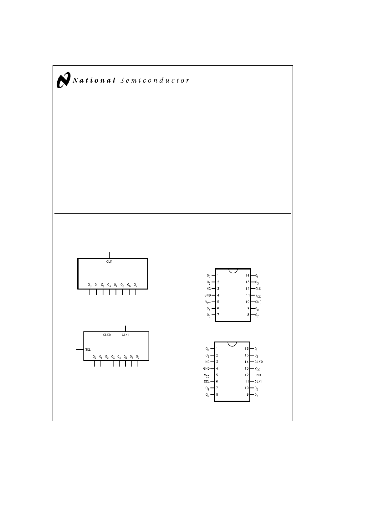
The CGS ’C/CT2525 is a minimum skew clock driver with
one input driving eight outputs specifically designed for signal generation and clock distribution applications. The ’2525
is designed to distribute a single clock to eight separate
receivers with low skew across all outputs during both the
t
PLH
and t
PHL
transitions. The ’2526 is similar to the ’2525
but contains a multiplexed clock input to allow for systems
with dual clock speeds or systems where a separate test
clock has been implemented.
Features
Y
These CGS devices implement National’s FACT
TM
family
Y
Ideal for signal generation and clock distribution
Y
Guaranteed pin to pin and part to part skew
Y
Multiplexed clock input (’2526)
Y
Guaranteed 2 kV minimum ESD protection
Y
Symmetric output current drive of 24 mA for IOL/I
OH
Y
’CT has TTL-compatible inputs
Y
These products are identical to 74AC/ACT2525 and
2526
Y
Available as Mil/Aero versions
54AC/ACT2525
54AC/ACT2526
Logic Symbols
’2525
TL/F/10684– 1
’2526
TL/F/10684– 2
Connection Diagrams
Pin Assignment
for DIP and SOIC
’2525
TL/F/10684– 3
’2526
TL/F/10684– 4
TRI-STATEÉis a registered trademark of National Semiconductor Corporation.
FACT
TM
is a trademark of National Semiconductor Corporation.
C
1996 National Semiconductor Corporation RRD-B30M106/Printed in U. S. A.
http://www.national.com
Page 2
Functional Description
On the multiplexed clock device, the SEL pin is used to
determine which CLKn input will have an active effect on
the outputs of the circuit. When SEL
e
1, the CLK1 input is
selected and when SEL
e
0, the CLK0 input is selected.
The non-selected CLKn input will not have any effect on the
logical output level of the circuit. The output pins act as a
single entity and will follow the state of the CLK or
CLK1/CLK0 pins when either the multiplexed (’2526) or the
straight (’2525) clock distribution chip is selected.
Pin Description
Pin Names Description
CLK Clock Input (’2525)
CLK0, CLK1 Clock Inputs (’2526)
O
0–O7
Outputs
SEL Clock Select (’2526)
Truth Tables
’2525
Inputs Outputs
CLK O0–O
7
LL
HH
’2526
Inputs Outputs
CLK0 CLK1 SEL O0–O
7
LXL L
HXL H
XLH L
XHH H
L
e
Low Voltage Level
H
e
High Voltage Level
X
e
Immaterial
’2525
TL/F/10684– 7
’2526
TL/F/10684– 8
http://www.national.com 2
Page 3
Absolute Maximum Ratings (Note 1)
If Military/Aerospace specified devices are required,
please contact the National Semiconductor Sales
Office/Distributors for availability and specifications.
Supply Voltage (V
CC
)
b
0.5V toa7.0V
DC Input Diode Current (IIK)
V
I
eb
0.5V
b
20 mA
V
I
e
V
CC
a
0.5V
a
0.2 mA
DC Input Voltage (VI)
b
0.5V to (V
CC
a
0.5V)
DC Output Diode Current (IOK)
V
O
e
0.5V
b
20 mA
V
O
e
V
CC
a
0.5V
a
20 mA
DC Output Voltage (VO)
b
0.5V to (V
CC
a
0.5V)
DC Output Source
or Sink Current (I
O
)
g
50 mA
DC VCCor Ground Current
per Output Pin (I
CC
or I
GND
)
g
50 MA
Storage Temperature (T
STG
)
b
65§Ctoa150§C
Junction Temperature (i
JA
)
Plastic (N) 14-Lead 102
§
C/W
Plastic (M) 14-Lead 128
§
C/W
Plastic (N) 16-Lead 97
§
C/W
Plastic (M) 16-Lead 124
§
C/W
Recommended Operating
Conditions
Supply Voltage (VCC)
‘C’ 2.0V to 6.0V
‘CT’ 4.5V to 5.5V
Input Voltage (V
I
) 0VtoV
CC
Output Voltage (VO) 0VtoV
CC
Operating Temperature (TA)
CGS74C/CT
b
40§Ctoa85§C
54AC/ACT
b
55§Ctoa125§C
Input Rise and Fall Times Devices
(30% to 70% of V
CC
)
V
CC
e
3.3V 10.5 ns max
4.5V 14.4 ns max
5.5V 17.6 ns max
Input Rise and Fall Times Devices
(0.8V to 2.0V) 9.6 ns max
Note 1: Absolute maximum ratings are those values beyond which damage
to the device may occur. The databook specifications should be met, without
exception, to ensure that the system design is reliable over its power supply,
temperature, and output/input loading variables. National does not recommend operation of CGS circuits outside databook specifications.
DC Electrical Characteristics for CGS74C and 54AC Family Devices
Over recommended operating conditions unless specified otherwise.
CGS74C 54AC CGS74C
Symbol Parameter
V
CC
T
A
ea
25§C
T
A
e
T
A
e
Units Conditions
(V)
b
55§Ctoa125§Cb40§Ctoa85§C
Typ Guaranteed Limits
V
IH
Minimum High Level 3.0 1.5 2.1 2.1 2.1 V
OUT
e
0.1V
Input Voltage 4.5 2.25 3.15 3.15 3.15 V or V
CC
b
0.1V
5.5 2.75 3.85 3.85 3.85
V
IL
Maximum Low Level 3.0 1.5 0.9 0.9 0.9 V
OUT
e
0.1V
Input Voltage 4.5 2.25 1.35 1.35 1.35 V or V
CC
b
0.1V
5.5 2.75 1.65 1.65 1.65
V
OH
Minimum High Level 3.0 2.99 2.9 2.9 2.9 I
OUT
eb
50 mA
Output Voltage 4.5 4.49 4.4 4.4 4.4 V
(Note 2) 5.5 5.49 5.4 5.4 5.4
V
IN
e
VILor V
IH
3.0 2.56 2.4 2.46
b
12 mA
4.5 3.86 3.7 3.76 V I
OH
b
24 mA
5.5 4.86 4.7 4.76
b
24 mA
V
OL
Maximum Low Level 3.0 0.002 0.1 0.1 0.1 I
OUT
e
50 mA
Output Voltage 4.5 0.001 0.1 0.1 0.1 V
(Note 2) 5.5 0.001 0.1 0.1 0.1
V
IN
e
VILor V
IH
3.0 0.36 0.40 0.44 12 mA
4.5 0.36 0.50 0.44 V
I
OL
24 mA
5.5 0.36 0.50 0.44 24 mA
http://www.national.com3
Page 4

DC Electrical Characteristics for CGS74C and 54AC Family Devices (Continued)
Over recommended operating conditions unless specified otherwise.
CGS74C 54AC CGS74C
Symbol Parameter
V
CC
T
A
ea
25§C
T
A
e
T
A
e
Units Conditions
(V)
b
55§Ctoa125§Cb40§Ctoa85§C
Typ Guaranteed Limits
I
IN
Maximum Input
5.5
g
0.1
g
1.0
g
1.0 mA
Leakage Current V
I
e
VCC, GND
(Note 3)
I
OLD
Minimum Dynamic 5.5 50 75 mA V
OLD
e
1.65V Max
I
OHD
Output Current
5.5
b
50
b
75 mA V
OHD
e
3.85V Min
(Note 4)
I
CC
Maximum Quiescent
5.5 8.0 80.0 80.0
mA
V
IN
e
V
CC
Supply Current
or GND
(Note 3)
DC Electrical Characteristics for CGS74CT and 54ACT Family Devices
Over recommended operating conditions unless specified otherwise.
CGS74CT 54ACT CGS74CT
Symbol Parameter
V
CC
T
A
ea
25§C
T
A
e
T
A
e
Units Conditions
(V)
b
55§Ctoa125§Cb40§Ctoa85§C
Typ Guaranteed Limits
V
IH
Minimum High Level 4.5 1.5 2.0 2.0 2.0
V
V
OUT
e
0.1V
Input Voltage 5.5 1.5 2.0 2.0 2.0 or V
CC
b
0.1V
V
IL
Maximum Low Level 4.5 1.5 0.8 0.8 0.8
V
V
OUT
e
0.1V
Input Voltage 5.5 1.5 0.8 0.8 0.8 or V
CC
b
0.1V
V
OH
Minimum High Level 4.5 4.49 4.4 4.4 4.4
VI
OUT
eb
50 mA
Output Voltage 5.5 5.49 5.4 5.4 5.4
(Note 2)
V
IN
e
VILor V
IH
4.5 3.86 3.70 3.76 V
I
OH
b
24 mA
5.5 4.86 4.70 4.76
b
24 mA
V
OL
Maximum Low Level 4.5 0.001 0.1 0.1 0.1
VI
OUT
e
50 mA
Output Voltage 5.5 0.001 0.1 0.1 0.1
(Note 2)
V
IN
e
VILor V
IH
4.5 0.36 0.50 0.44 V
I
OL
24 mA
5.5 0.36 0.50 0.44 24 mA
I
IN
Maximum Input
5.5
g
0.1
g
1.0
g
1.0 mAV
I
e
VCC, GND
Leakage Current
I
CCT
Maximum ICC/Input 5.5 0.6 1.6 1.5 mA V
I
e
V
CC
b
2.1V
I
OLD
Minimum Dynamic 5.5 50 75 mA V
OLD
e
1.65V Max
I
OHD
Output Current
5.5
b
50
b
75 mA V
OHD
e
3.85V Min
(Note 4)
I
CC
Maximum Quiescent
5.5 8.0 160.0 80.0 mA
V
IN
e
V
CC
Supply Current
or GND
(Note 5)
http://www.national.com 4
Page 5

AC Electrical Characteristics Over recommended operating conditions unless specified otherwise.
(Note 6)
Range
V
CC
(V)
CGS74C 54AC CGS74C
T
A
ea
25§C
T
A
eb
55§CT
A
eb
40§C
Symbol Parameter
C
L
e
50 pF
to
a
125§Cto
a
85§C Units
C
L
e
50 pF C
L
e
50 pF
Min Typ Max Min Max Min Typ Max
t
PLH
, Propagation Delay 3.3 3.0 6.5 11.0 3.0 11.0 3.0 12.5
ns
t
PHL
CLK to On(’2525) 5.0 3.2 5.0 7.8 2.5 8.2 2.9 8.1
t
PLH,
Propagation Delay 3.3 3.0 7.0 13.0 3.0 14.0
ns
t
PHL
CLKn to On(’2526) 5.0 3.6 5.5 7.8 3.3 8.6
t
PLH
, Propagation Delay 3.3 3.0 8.0 14.0 3.0 15.0
ns
t
PHL
SEL to On(’2526) 5.0 4.0 6.5 8.5 3.5 9.5
t
OSHL
Maximum Skew
3.3 0.3 1.5 600
Common Edge
ps
Output-to-Output (Note 7)
5.0 0.2 1.0 500
Variation
t
OSLH
Maximum Skew
3.3 0.3 1.5 600
Common Edge
ps
Output-to-Output (Note 7)
5.0 0.2 1.0 500
Variation
t
OST
Maximum Skew
1.5
Opposite Edge
5.0 0.4 1.0 1.0 ns
Output-to-Output (Note 7)
1.0
Variation
t
PV
Maximum Skew ’C2525
Part-to-Part ’CT2525 5.0 3.5 4.0 ns
Variation (Note 8) ’C2526
’CT2526 5.0 5.0 ns
t
rise
, Maximum
t
fall
Rise/Fall Time 5.0 3.0 4.0 3.75 ns
(20% to 80% V
CC
)
t
rise
, Maximum
t
fall
Rise/Fall Time 0.9 1.1 ns
(0.8V/2.0V and 2.0V/0.8V)
AC Electrical Characteristics Over recommended operating conditions unless specified otherwise.
(Note 6)
Range
V
CC
(V)
CGS74CT 54ACT CGS74CT
T
A
ea
25§C
T
A
eb
55§CT
A
eb
40§C
Symbol Parameter
C
L
e
50 pF
to
a
125§Cto
a
85§C Units
C
L
e
50 pF C
L
e
50 pF
Min Typ Max Min Max Min Max
t
PLH
, Propagation Delay
5.0 4.6 6.5 9.0 4.0 10.1 ns
t
PHL
CLK to On(’2525)
t
PLH,
Propagation Delay
5.0 5.8 8.5 11.1 5.1 12.4 ns
t
PHL
CLKn to On(’2526)
http://www.national.com5
Page 6

AC Electrical Characteristics
Over recommended operating conditions unless specified otherwise. (Continued)
(Note 6)
Range
V
CC
(V)
CGS74CT 54ACT CGS74CT
T
A
ea
25§C
T
A
eb
55§CT
A
eb
40§C
Symbol Parameter
C
L
e
50 pF
to
a
125§Cto
a
85§C Units
C
L
e
50 pF C
L
e
50 pF
Min Typ Max Min Max Min Typ Max
t
PLH
, Propagation Delay
5.0 5.1 8.5 12.4 4.4 14.1 ns
t
PHL
SEL to On(’2526)
t
OSHL
Maximum Skew
Common Edge
5.0 0.2 550 ps
Output-to-Output (Note 7)
Variation
t
OSLH
Maximum Skew
Common Edge
5.0 0.2 550 ps
Output-to-Output (Note 7)
Variation
t
OST
Maximum Skew
Opposite Edge
5.0 0.4 1.0 ns
Output-to-Output (Note 7)
Variation
t
PV
Maximum Skew AC2525
Part-to-Part ACT2525
Variation (Note 8) AC2526 5.0 3.5 ns
ACT2526 5.0 5.0 ns
t
rise
, Maximum
t
fall
Rise/Fall Time 5.0 3.0 3.75 ns
(20% to 80% V
CC
)
t
rise
, Maximum
t
fall
Rise/Fall Time 0.9 1.1 ns
(0.8V/2.0V and 2.0V/0.8V)
Note 2: All outputs loaded; thresholds on input associated with output under test.
Note 3: I
IN
and I
CC
@
3.0V are guaranteed to be less than or equal to the respective limit@5.5V VCC.
I
CC
for 54AC@25§C is identical to CGS74C@25§C.
Note 4: Maximum test duration 2.0 ms, one output loaded at a time.
Note 5: I
CC
for 54ACT@25§C is identical to CGS74CT@25§C.
Note 6: Voltage Range 5.0 is 5.0V
g
0.5V, voltage range 3.3 is 3.3Vg0.3V.
Note 7: Output-to-Output Skew is defined as the absolute value of the difference between the actual propagation delay for any outputs within the same packaged
device. The specifications apply to any outputs switching in the same direction either HIGH to LOW (t
OSHL
) or LOW to HIGH (t
OSLH
) or in opposite directions both
HL and LH (t
OST
). t
OSHL
and t
OSLH
are characterized and guaranteed by design@1 MHz.
Note 8: Part-to-part skew is defined as the absolute value of the difference between the propagation delay for any outputs from device to device. The parameter is
specified for a given set of conditions (i.e., capacitive load, V
CC
, temperature,Ýof outputs switching, etc.). Parameter guaranteed by design.
Note 9: Load capacitance includes the test jig.
http://www.national.com 6
Page 7

Capacitance
Symbol Parameter Typ Units Conditions
C
IN
Input Capacitance 4.5 pF V
CC
e
5.0V
C
PD
Power Dissipation Capacitance (’2525) 820 pF–1.2 x 10
b
18
(f)* pF V
CC
e
5.0V
C
PD
Power Dissipation Capacitance (’2526) 820 pF–1.2 x 10
b
18
(f)* pF V
CC
e
5.0V
*fefrequency
Recommended Maximum Power Dissipation (W)
LFPM
T
A
e
25§CT
A
e
85§C
PDIP SOIC PDIP SOIC
0 1.105 0.858 0.528 0.41
225 1.493 1.055 0.714 0.504
500 1.71 1.210 0.820 0.578
Timing Diagrams
TL/F/10684– 27
TL/F/10684– 28
Test Circuit
TL/F/10684– 29
RLis 500X
C
L
is 50 pF for all prop delays and skew measurements.
http://www.national.com7
Page 8

Ordering Information
The device number is used to form part of a simplified purchasing code where the package type and temperature range are
defined as follows:
TL/F/10684– 26
Physical Dimensions inches (millimeters) unless otherwise noted
14-Lead Small Outline Integrated Circuit (M)
NS Package Number M14A
http://www.national.com 8
Page 9

Physical Dimensions inches (millimeters) unless otherwise noted (Continued)
16-Lead Small Outline Integrated Circuit (M)
NS Package Number M16A
14-Lead Plastic Dual-In-Line Package (N)
NS Package Number N14A
http://www.national.com9
Page 10

CGS74C2525
#
CGS74CT2525
#
CGS74C2526
#
CGS74CT2526
1-to-8 Minimum Skew Clock Driver
Physical Dimensions inches (millimeters) unless otherwise noted (Continued)
16-Lead Plastic Dual-In-Line Package (N)
NS Package Number N16E
LIFE SUPPORT POLICY
NATIONAL’S PRODUCTS ARE NOT AUTHORIZED FOR USE AS CRITICAL COMPONENTS IN LIFE SUPPORT
DEVICES OR SYSTEMS WITHOUT THE EXPRESS WRITTEN APPROVAL OF THE PRESIDENT OF NATIONAL
SEMICONDUCTOR CORPORATION. As used herein:
1. Life support devices or systems are devices or 2. A critical component is any component of a life
systems which, (a) are intended for surgical implant support device or system whose failure to perform can
into the body, or (b) support or sustain life, and whose be reasonably expected to cause the failure of the life
failure to perform, when properly used in accordance support device or system, or to affect its safety or
with instructions for use provided in the labeling, can effectiveness.
be reasonably expected to result in a significant injury
to the user.
National Semiconductor National Semiconductor National Semiconductor National Semiconductor
Corporation Europe Hong Kong Ltd. Japan Ltd.
1111 West Bardin Road Fax:
a
49 (0) 180-530 85 86 13th Floor, Straight Block, Tel: 81-043-299-2308
Arlington, TX 76017 Email: europe.support@nsc.com Ocean Centre, 5 Canton Rd. Fax: 81-043-299-2408
Tel: 1(800) 272-9959 Deutsch Tel:
a
49 (0) 180-530 85 85 Tsimshatsui, Kowloon
Fax: 1(800) 737-7018 English Tel:
a
49 (0) 180-532 78 32 Hong Kong
Fran3ais Tel:
a
49 (0) 180-532 93 58 Tel: (852) 2737-1600
http://www.national.com
Italiano Tel:a49 (0) 180-534 16 80 Fax: (852) 2736-9960
National does not assume any responsibility for use of any circuitry described, no circuit patent licenses are implied and National reserves the right at any time without notice to change said circuitry and specifications.
 Loading...