

Page 1
TL/F/11752
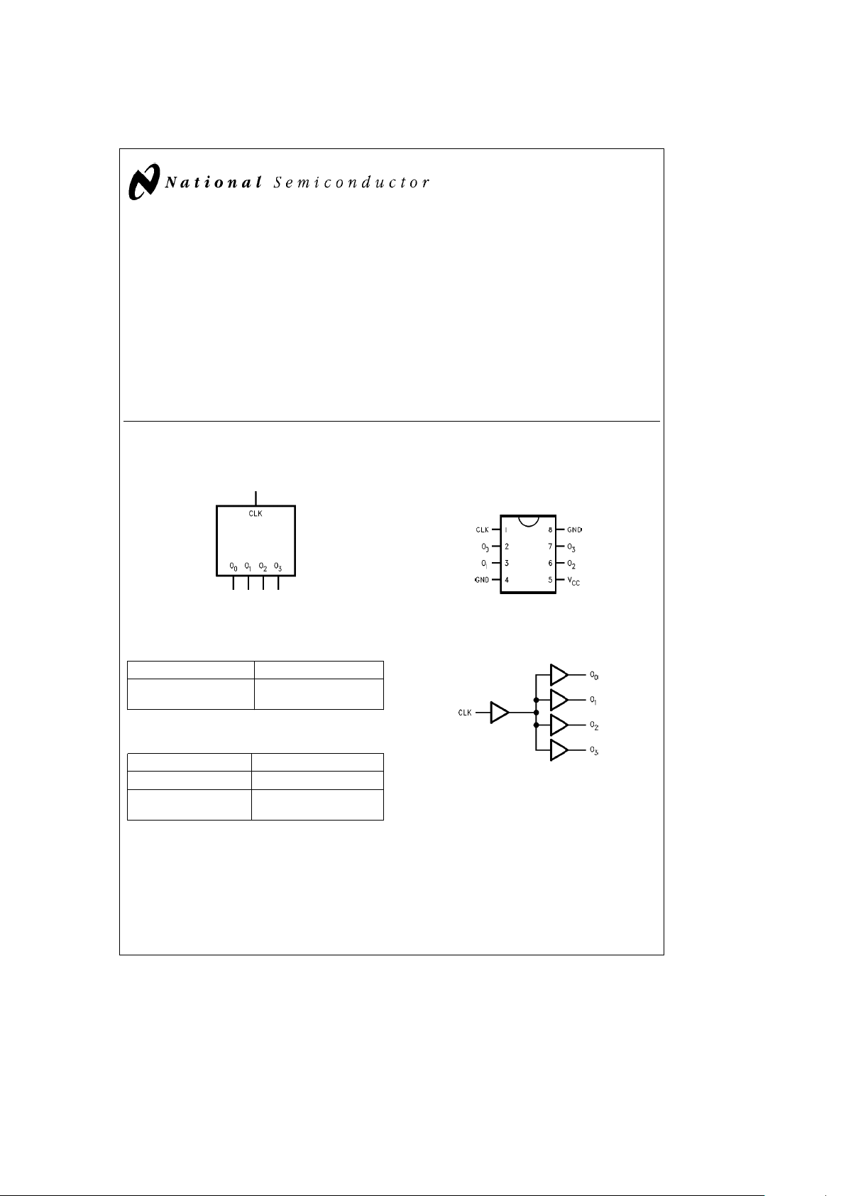
CGS74CT2524 1 to 4 Minimum Skew (300 ps) Clock Driver
September 1995
CGS74CT2524
1 to 4 Minimum Skew (300 ps) Clock Driver
General Description
These minimum skew clock drivers are designed for Clock
Generation and Support (CGS) applications operating at
high frequencies. This device guarantees minimum output
skew across the outputs of a given device.
Skew parameters are also provided as a means to measure
duty cycle requirements as those found in high speed clocking systems. The CGS74CT2524 is a minimum skew clock
driver with one input driving four outputs, specifically designed for signal generation and clock distribution applications.
Features
Y
Guaranteed 300 ps pin-to-pin skew (t
OSHL
and t
OSLH
)
Y
Implemented on National’s FACTTMfamily process
Y
1 input to 4 outputs low skew clock distribution
Y
Symmetric output current drive: 24 mA IOH/I
OL
Y
Industrial temperature ofb40§Ctoa85§C
Y
8-pin SOIC package
Y
Low dynamic power consumption above 20 MHz
Y
Guaranteed 2 kV ESD protection
Logic Symbol
TL/F/11752– 1
The output pins act as a single entity and will follow the state of the CLK
when the clock distribution chip is selected.
Pin Description
Pin Names Descripton
CLK Clock Input
O
0–O3
Outputs
Truth Table
Inputs Outputs
CLK O0–O
3
LL
HH
L
e
Low Logic Level
H
e
High Logic Level
Connection Diagrams
Pin Assignment
SOIC (M)
TL/F/11752– 2
TL/F/11752– 3
FACTTMis a trademark of National Semiconductor Corporation.
C
1995 National Semiconductor Corporation RRD-B30M115/Printed in U. S. A.
Page 2
Absolute Maximum Ratings (Note)
If Military/Aerospace specified devices are required,
please contact the National Semiconductor Sales
Office/Distributors for availability and specifications.
Supply Voltage (V
CC
)
b
0.5 to 7.0V
DC Input Voltage Diode Current (IIK)
V
eb
0.5V
b
20 mA
V
e
V
CC
a
0.5V
a
20 mA
DC Input Voltage (VI)
b
0.5V to (V
CC
a
0.5V)
DC Output Diode (Current) (IO)
V
eb
0.5V
b
20 mA
V
e
V
CC
a
0.5V
a
20 mA
DC Output Voltage (VO)
b
0.5V to (V
CC
a
0.5V)
DC Output Source
or Sink Current (I
O
)
g
50 mA
DC VCCor Ground Current
per Output Pin (I
CC
or I
GND
)
g
50 mA
Storage Temperature (T
STG
)
b
65§Ctoa150§C
Junction Temperature (i
JA
) 0 225 500 LFM
M 167 132 117
§
C/W
N 115 79 62
§
C/W
Recommended Operating
Conditions
Supply Voltage (VCC) 4.5V to 5.5V
Input Voltage (VI) 0VtoV
CC
Output Voltage (VO) 0 to V
CC
Operating Temperature (TA)
b
40§Ctoa85§C
Input Rise and Fall Times
(0.8V to 2.0V) 9.6 ns max
NOTE:
The Absolute Maximum Ratings are those values
beyond which the safety of the device cannot be guaranteed. The device should not be operated at these limits. The
parametric values defined in the DC and AC Electrical Characteristics tables are not guaranteed at the absolute maximum ratings. The Recommended Operating Conditions will
define the conditions for actual device operation.
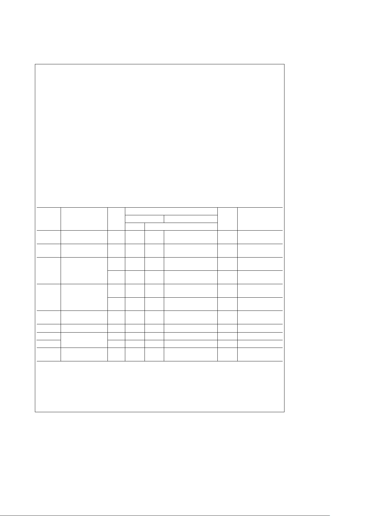
DC Electrical Characteristics
Over recommended operating conditions unless specified otherwise.
Symbol Parameter
V
CC
(V)
CGS74CT2524
Units Conditions
T
A
ea
25§CT
A
eb
40§Ctoa85§C
Typ Guaranteed Limits
V
IH
Minimum High Level 4.5 1.5 2.0 2.0
V
V
OUT
e
0.1V
Input Voltage 5.5 1.5 2.0 2.0 or V
CC
eb
0.1V
V
IL
Maximum Low Level 4.5 1.5 0.8 0.8
V
V
OUT
e
0.1V
Input Voltage 5.5 1.5 0.8 0.8 or V
CC
eb
0.1V
V
OH
Minimum High Level 4.5 4.49 4.4 4.4
V
V
IN
e
V
IH
Output Voltage 5.5 5.49 5.4 5.4 I
OUT
eb
50 mA
4.5 3.86 3.76
V
V
IN
e
V
IH
5.5 4.86 4.76 I
OH
eb
24 mA
V
OL
Minimum Low Level 4.5 0.001 0.1 0.1
V
V
IN
e
V
IL
Output Voltage 5.5 0.001 0.1 0.1 I
OUT
e
50 mA
4.5 0.36 0.44
V
V
IN
e
V
IL
5.5 0.36 0.44 I
OL
e
24 mA
I
IN
Maximum Input
5.5
g
0.1
g
1.0 mA
V
I
e
VCC, GND
Leakage Current
I
CC
T
Maximum ICC/Input 5.5 0.6 1.5 mA V
I
e
V
CC
b
2.1V
I
OLD
Minimum Dynamic 5.5 75 mA V
OLD
e
1.65V Max
I
OHD
Output Current
5.5
b
75 mA V
OHD
e
3.85V Min
I
CC
Maximum Quiescent
5.5 8.0 80 mA
V
IN
e
V
CC
Supply Current or GND
2
Page 3

AC Electrical Characteristics
Over recommended operating conditions unless specified otherwise. All typical values are measured at V
CC
e
5V, T
A
e
25§C.
Symbol Parameter
CGS74CT2524
Units
V
CC
e
4.5V to 5.5V
T
A
eb
40§Ctoa85§C
C
L
e
50 pF
R
L
e
500X
Min Typ Max
t
PLH
Low-to-High Propagation Delay
3.5 9.0 ns
CLK to O
n
t
PHL
High-to-Low Propagation Delay
3.5 9.0 ns
CLK to O
n
Extended AC Electrical Characteristics
Over recommended operating conditions unless specified otherwise. All typical values are measured at V
CC
e
5V, T
A
e
25§C.
Symbol Parameter
CGS74CT2524
Units
V
CC
e
4.5V to 5.5V
T
A
eb
40§Ctoa85§C
C
L
e
50 pF
R
L
e
500X
Package Min Typ Max
F
max
Maximum Operating Frequency 100 MHz
t
OSHL
Maximum Skew Common Edge M 300
Output-to-Output Variation (Note 1) M (Note 2) 450 ps
N 500
t
OSLH
Maximum Skew Common Edge M 300
Output-to-Output Variation (Note 1) M (Note 2) 450 ps
N 500
t
PS
Maximum Skew Pin (Signal)
1.0 ns
Transition Variation (Note 3)
t
rise
Rise Time/Fall Time
1.5 ns
t
fall
(from 0.8V to 2.0V/2.0V to 0.8V)
T
High
Time High 4 ns
T
Low
Time Low 4 ns
Note 1: Output-to-Output Skew is defined as the absolute value of the difference between the actual propagation delay from any outputs within the same packaged
device. The specifications apply to any outputs switching in the same direction either HIGH to LOW (t
OSHL
) or LOW to HIGH (t
OSLH
) or in opposite directions both
HL and LH (t
OST
). t
OSHL
and t
OSLH
are characterized and guaranteed by design@1 MHz.
Note 2: Characterized at 66 MHz. Parameter guaranteed by design.
Note 3: Pin transition skew is the absolute difference between High-to-Low and Low-to-High propagation delay measure at a given output pin.
Note 4: Load capacitance includes the test jig.
3
Page 4

Timing Diagrams
1 to 4 Min-Skew Clock Driver
TL/F/11752– 4
TL/F/11752– 5
TL/F/11752– 13
Time high is measured with outputs above 2V.
Time low is measured with outputs below 0.8V.
Test Circuit
TL/F/11752– 6
RLis 500X
C
L
is 50 pF for all prop delays and skew measurements.
4
Page 5

Ordering Information
Contact NSC Marketing for specific data of availability
TL/F/11752– 14
5
Page 6

CGS74CT2524 1 to 4 Minimum Skew (300 ps) Clock Driver
Physical Dimensions inches (millimeters)
8 Lead (0.150×Wide) Molded Small Outline Package (M)
NS Package Number M08A
LIFE SUPPORT POLICY
NATIONAL’S PRODUCTS ARE NOT AUTHORIZED FOR USE AS CRITICAL COMPONENTS IN LIFE SUPPORT
DEVICES OR SYSTEMS WITHOUT THE EXPRESS WRITTEN APPROVAL OF THE PRESIDENT OF NATIONAL
SEMICONDUCTOR CORPORATION. As used herein:
1. Life support devices or systems are devices or 2. A critical component is any component of a life
systems which, (a) are intended for surgical implant support device or system whose failure to perform can
into the body, or (b) support or sustain life, and whose be reasonably expected to cause the failure of the life
failure to perform, when properly used in accordance support device or system, or to affect its safety or
with instructions for use provided in the labeling, can effectiveness.
be reasonably expected to result in a significant injury
to the user.
National Semiconductor National Semiconductor National Semiconductor National Semiconductor
Corporation Europe Hong Kong Ltd. Japan Ltd.
1111 West Bardin Road Fax: (
a
49) 0-180-530 85 86 13th Floor, Straight Block, Tel: 81-043-299-2309
Arlington, TX 76017 Email: cnjwge@tevm2.nsc.com Ocean Centre, 5 Canton Rd. Fax: 81-043-299-2408
Tel: 1(800) 272-9959 Deutsch Tel: (
a
49) 0-180-530 85 85 Tsimshatsui, Kowloon
Fax: 1(800) 737-7018 English Tel: (
a
49) 0-180-532 78 32 Hong Kong
Fran3ais Tel: (
a
49) 0-180-532 93 58 Tel: (852) 2737-1600
Italiano Tel: (
a
49) 0-180-534 16 80 Fax: (852) 2736-9960
National does not assume any responsibility for use of any circuitry described, no circuit patent licenses are implied and National reserves the right at any time without notice to change said circuitry and specifications.
 Loading...