

Page 1
3236 Scott Boulevard Santa Clara, California 95054 Phone: (408) 986-5060 Fax: (408) 986-5095
CFK2062-P1
Features
❏ High Gain
❏ +30 dBm Power Output
❏ Proprietary Power FET Process
❏ >40% Linear Power Added Efficiency
❏ Surface Mount SO-8 Power Package
Applications
❏ ISM Band Base Stations and Terminals
❏ Cellular Base Stations and Terminals
❏ Wireless Local Loop
Description
The CFK2062-P1 is a high-gain FET intended for driver amplifier applications in high-power systems, and output
stage usage in medium power applications at power levels up to
+30 dBm. The device is easily matched and provides excellent
linearity at 1 Watt. Manufactured in Celeritek’s proprietary
power FET process, this device is assembled in an industry
standard surface mount SO-8 power package that is compatible
with high volume, automated board assembly techniques.
800 to 900 MHz
+30 dBm Power GaAs FET
Product Specifications
December 1997 (1 of 4)
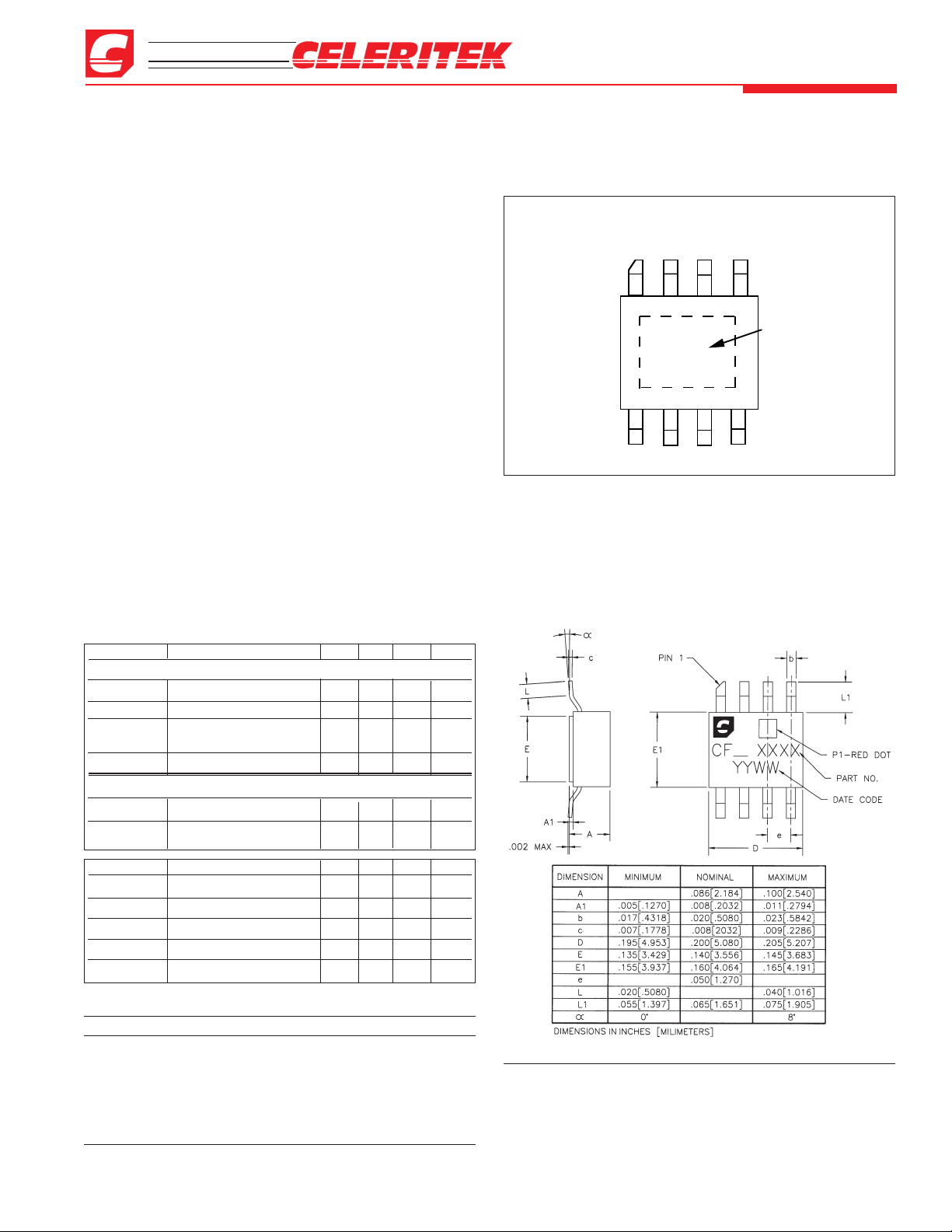
13478652GGD
D
Back Plane
is Source
GND
GND
GND
GND
Package Diagram
Absolute Maximum Ratings
Parameter Symbol Rating
Drain-Source Voltage V
DS
10V
(3)
Gate-Source Voltage V
GS
-5V
Drain Current I
DS
Idss
Continuous Dissipation P
T
6W
Channel Temperature T
CH
175°C
Storage Temperature T
STG
-65°C to +175°C
SO-8 Power Package Physical Dimensions
Notes:
1. Sum to two tones with 1 MHz spacing = 25 dBm.
2. See thermal considerations information on page 4.
3. Maximum potential difference across the device (Vd + Vg) cannot
exceed 12V.
Parameters Conditions Min Typ Max Units
Vd= 8V, Id= 400 mA (Quiescent)
P
-1 dB
29.0 30.0 — dBm
SSG 18.0 20.0 — dB
3rd Order
Products
(1)
—30— dBc
Efficiency @ P1dB — 40 — %
Vd= 5V, Id= 600 mA (Quiescent)
P
-1 dB
— 29.5 — dBm
SSG — 19.0 — dB
Specifications (TA = 25°C)
The following specifications are
guaranteed at room temperature in Celeritek test fixture at 850 MHz.
Parameters Conditions Min Typ Max Units
g
m
Vds = 2.0V, Vgs = 0V — 650 — mS
I
dss
Vds = 2.0V, Vgs = 0V — 1.4 — A
V
p
Vds = 3.0V, Ids = 25 mA — -1.8 Volts
BV
GD
Igd = 2.5 mA 15 17 — Volts
ΘJL(2) @150°C TCH — 12 — °C/W
Page 2
3236 Scott Boulevard, Santa Clara, California 95054
Phone: (408) 986-5060 Fax: (408) 986-5095
CFK2062-P1
Product Specifications - December 1997
(2 of 4)
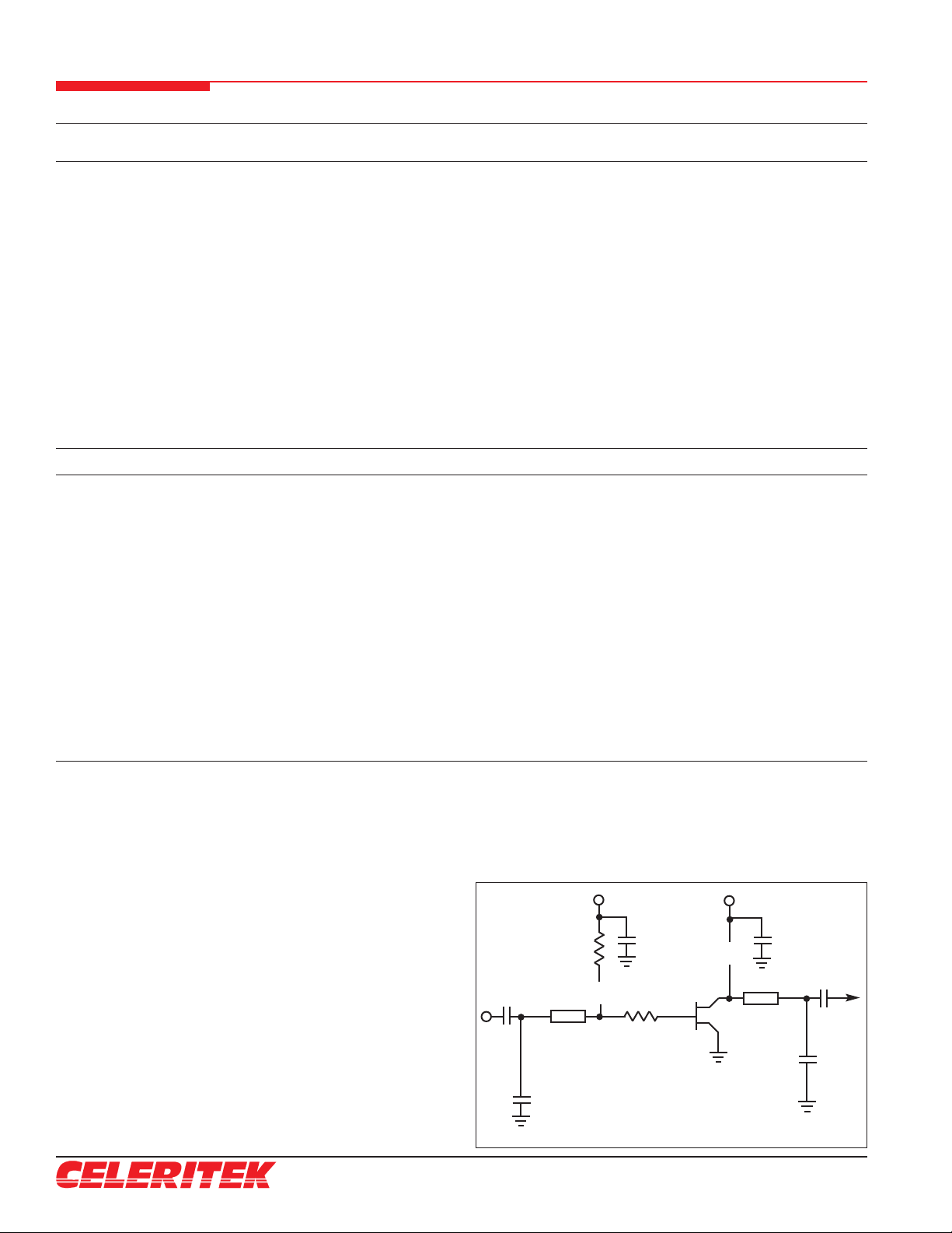
RF Match Data shown in the performance graphs was taken
in the test circuit shown at right. Layout is important for proper operation. Phase length of input and output 50Ω line varies
as a function of exact desired frequency of operation. Output
shunt inductor effects output performance. Celeritek recommends the use of a high impedance printed inductor
Lambda/4 in length.Please contact the factory for an evaluation board and/or more detailed application support.
Typical Scattering Parameters (TA = 25°C, Vds = 5 V, Ids = 600 mA)
Frequency S
11
S
21
S
12
S
22
(GHz) Mag Ang Mag Ang Mag Ang Mag Ang
0.6 0.927 -129.75 8.7 102.7 0.024 21.95 0.576 -178.45
0.7 0.921 -138.64 7.587 97.2 0.025 16.98 0.588 179.24
0.8 0.919 -145.3 6.726 92.32 0.025 12.77 0.597 177.37
0.9 0.919 -150.58 6.02 88.2 0.025 12.07 0.6 176.07
1.0 0.914 -154.69 5.449 84.82 0.025 8.72 0.6 175.04
1.1 0.911 -157.8 5.018 82.03 0.026 7.57 0.597 174.42
1.2 0.91 -160.09 4.678 79.43 0.027 6.24 0.594 173.69
1.3 0.908 -162.37 4.423 76.85 0.027 4.79 0.588 172.66
1.4 0.904 -164.19 4.225 74.15 0.028 2.63 0.578 171.66
1.5 0.9 -166.3 4.066 71.35 0.029 2.62 0.567 170.4
2.0 0.883 177.09 3.605 52.62 0.05 -10.6 0.512 154.61
2.5 0.887 150.54 2.944 28.96 0.035 -30.13 0.539 128.94
3.0 0.917 135.01 2.081 13.19 0.03 -41.27 0.623 118.42
3.5 0.932 137.14 1.635 8.18 0.028 -41.69 0.643 124.18
4.0 0.913 143.42 1.641 3.36 0.032 -41.15 0.557 131.38
(TA = 25°C, Vds = 8 V, Ids = 400 mA)
0.6 0.91 -131.25 9.129 100.5 0.026 17.07 0.521 -174.04
0.7 0.905 -139.87 7.943 95.18 0.026 13.22 0.534 -176.65
0.8 0.906 -146.47 7.028 90.26 0.026 11.05 0.543 -178.82
0.9 0.906 -151.44 6.281 86.16 0.027 8.59 0.547 179.94
1.0 0.904 -155.33 5.68 82.61 0.027 6.34 0.548 178.8
1.1 0.903 -158.37 5.226 79.83 0.027 3.72 0.547 178.18
1.2 0.903 -160.69 4.866 77.15 0.027 3.34 0.544 177.57
1.3 0.899 -167.2 4.574 74.6 0.028 0.5 0.538 176.86
1.4 0.897 -164.68 4.366 71.76 0.029 1.6 0.53 176.13
1.5 0.892 -166.63 4.203 68.96 0.03 -0.36 0.519 174.97
2.0 0.877 176.74 3.696 50.36 0.035 -13.77 0.463 160.21
2.5 0.882 150.43 3.014 26.66 0.036 -31.65 0.486 133.49
3.0 0.915 135.06 2.136 10.26 0.031 -46.6 0.579 121.99
3.5 0.93 137.37 1.662 4.59 0.027 -43.86 0.611 128.44
4.0 0.912 143.75 1.642 -0.35 0.031 -43.95 0.541 137.64
RF
OUT
RF
IN
CFK2062-P1, 8V, 400 mA
50 Ω
uuuu
V
g
uuuu
100 pF
50 Ω
0.1 µF
5.1 Ω
0.1 µF
91 Ω
100
pF
V
d
6.8 pF
10 pF
47 nH
100 nH
Page 3

3236 Scott Boulevard Santa Clara, California 95054 Phone: (408) 986-5060 Fax: (408) 986-5095
Power Output & Power Added Efficiency vs Power Input
850 MHz, VDS = 5 V, IDS = 600 mA
Power Input (dBm)
Power Output (dBm)
Efficiency (%)
Efficiency
Power Output
515253545101520253035-505152010
55
Power Input (dBm)
Power Output & Power Added Efficiency vs Power Input
850 MHz, VDS = 8 V, IDS = 400 mA
Power Output (dBm)
Efficiency (%)
Efficiency
Power Output
01020304050101520253035-5051520
10
Gain @ P
-1 dB
Frequency, MHz
Power Output and Gain vs Frequency
VDS =8V, IDS = 400 mA
Power Output @ P
-1 dB
825
850
875
900
925
Gain20212223192829303132
Power Output
Frequency, MHz
Power Output @ P
-1 dB
Gain @ P
-1 dB
Power Output
1920212218
Gain28293031
32
Power Output and Gain vs Frequency
VDS =5V, IDS = 600 mA
825
875
925
850
900
Volts
Power Output and Gain vs Voltage @ 850 MHz
IDS = 400 mA
Power Output @ P
-1 dB
Gain @ P
-1 dB
Gain
Power Output
192225283134171819202122357468Volts
Power Output and Gain vs Voltage @ 850 MHz
IDS = 600 mA
Power Output @ P
-1 dB
Gain @ P
-1 dB
Gain
Power Output
1819202122233574682124273033
36
CFK2062-P1
Product Specifications - December 1997 (3 of 4)
Typical Performance
Page 4

3236 Scott Boulevard, Santa Clara, California 95054
Phone: (408) 986-5060 Fax: (408) 986-5095
CFK2062-P1
Product Specifications - December 1997
(4 of 4)
Celeritek reserves the right to make changes without further notice to any products herein. Celeritek makes no warranty, representation or guarantee regarding the
suitability of its products for any particular purpose, nor does Celeritek assume any liability arising out of the application or use of any product or circuit, and specifically
disclaims any and all liability, including without limitation consequential or incidental damages. “Typical” parameters can and do vary in different applications. All operating
parameters, including “Typicals” must be validated for each customer application by customer’s technical experts. Celeritek does not convey any license under its patent
rights nor the rights of others. Celeritek products are not designed, intended, or authorized for use as components in systems intended for surgical implant into the body, or
other applications intended to support or sustain life, or for any other application in which the failure of the Celeritek product could create a situation where personal injury
or death may occur. Should Buyer purchase or use Celeritek products for any such unintended or unauthorized application, Buyer shall indemnify and hold Celeritek and
its officers, employees, subsidiaries, affiliates, and distributors harmless against all claims, costs, damages, and expenses, and reasonable attorney fees arising out of,
directly or indirectly, any claim of personal injury or death associated with such unintended or unauthorized use, even if such claim alleges that Celeritek was negligent
regarding the design or manufacture of the part. Celeritek is a registered trademark of Celeritek, Inc. Celeritek, Inc. is an Equal Opportunity/Affirmative Action Employer.
Ordering Information
The CFK2062-P1 power stage is available in a SO-8 surface mount package. Devices are available in tape and reel. Ordering part
numbers are listed.
Part Number for Ordering Function Package
CFK2062-P1 800 - 900 MHz Power Stage SO-8 surface mount power package
CFK2062-P1-000T 800 - 900 MHz Power Stage SO-8 surface mount power package in tape and reel
Thermal Considerations
The data shown was taken on a 31 mil thick FR-4 board with 1 ounce copper on both sides. The board was mounted to a baseplate with 3 screws as shown. The screws bring the top side copper temperature to the same value as the baseplate. The thermal
resistance to the indicated reference lead, ΘJL, is 12°C/W. The thermal resistance to the reference screw is 14°C/W.
1. Use 1 or 2 ounce copper if possible.
2. Solder all eight leads of the CFK2062-P1 package to the appropriate electrical connection.
3. Solder the copper pad on the backside of the CFK2062-P1 package to the ground plane.
4. Use a large ground pad area with many plated through-holes as shown.
5. If possible, use at least one screw no more than 0.2 inches from the CFK2062-P1 package to provide a low thermal resistance
path to the baseplate of the package.
 Loading...