

Page 1
July 1997
CA3272A, CA3292A
Quad-Gated Inverting Power Drivers with Fault
Mode Diagnostic Flag Output
Features
• Load Current Switching 600mA
• Suitable for Resistive or Inductive Loads
• Fault Mode Diagnostic Flag Output
• CA3292A Over-Voltage Zener Clamp
• Independent Over-Current Limiting
• Independent Over-Temperature Shutdown
• Temperature Shutdown Hysteresis
• 5V CMOS or TTL Input Logic
• High Dissipation Power-Frame Package
o
• Operating Temperature Range -40
C to 125oC
Applications System Applications
• Solenoids • Automotive
• Relays • Appliance
• Lamps • Industrial Control
• Steppers • Robotics
• Injectors
• Motors
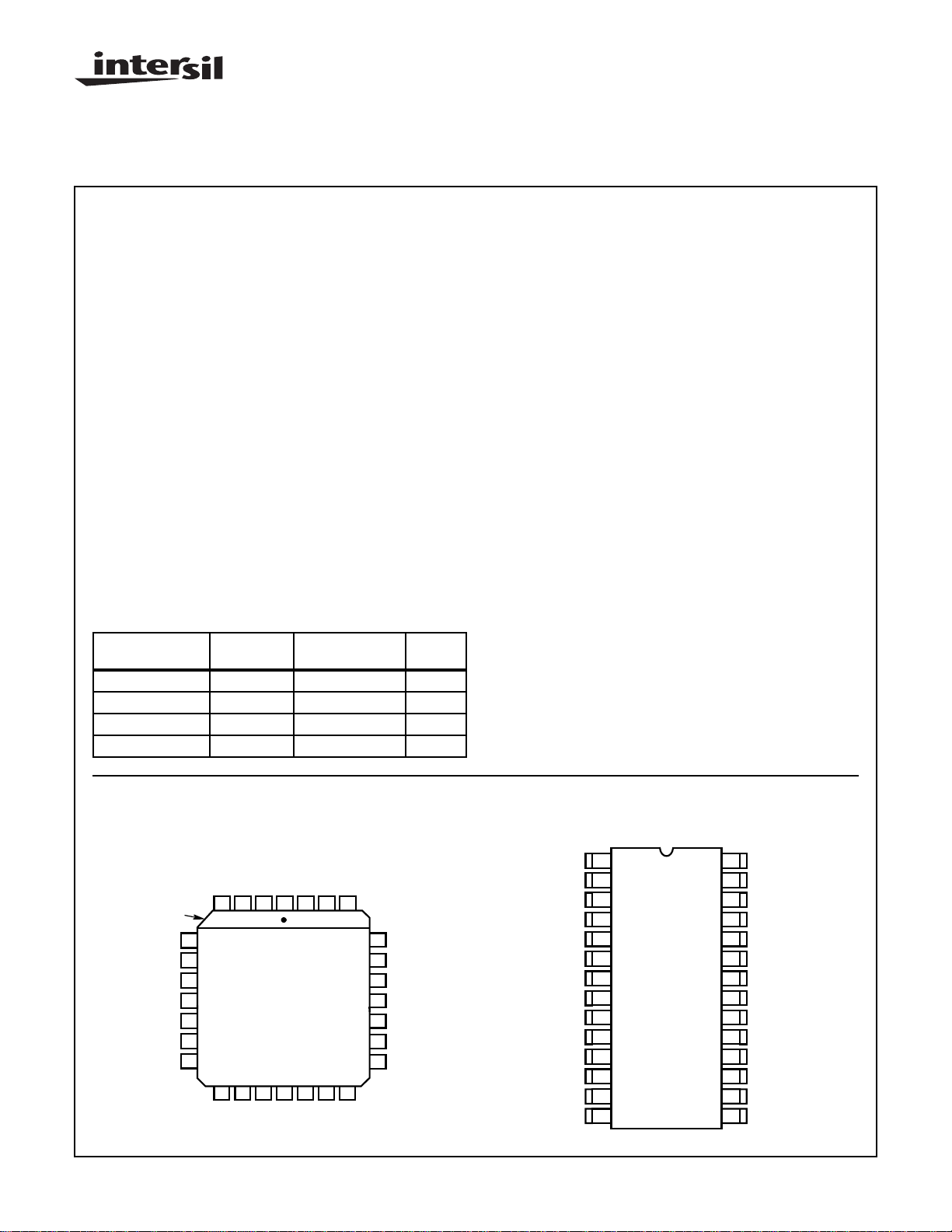
Ordering Information
TEMP.
PART NUMBER
CA3272AQ -40 to 125 28 Ld PLCC N28.45
CA3292AQ -40 to 125 28 Ld PLCC N28.45
CA3272AM -40 to 125 28 Ld SOIC M28.3
CA3292AM -40 to 125 28 Ld SOIC M28.3
RANGE (oC) PACKAGE
PKG.
NO.
Description
The CA3272A and CA3292A are Quad-Gated Inverting Power
Drivers for interfacing low-level logic to inductive and resistive
loads such as: relays, solenoids, AC and DC motors and resistive loads such as incandescent lamps and other power drivers .
Each output is an open collector protected power transistor
driver. The CA3292A is similar to the CA3272A, except for an
added collector-to-base Zener diode that provides over-voltage
clamping protection on each power switching output. The
CA3292A block diagram is shown for one switching channel
with fault detection logic plus the output fault driver circuit for all
four switching channels. The FAULT output pin provides a flag
output when a fault condition occurs. All four Output Power
Driver stages are shown in the Block Diagrams .
The ENABLE input is common to each of the four power
switches and when low, disables the FAULT output. From the
Input to Output, each switch is inverting. When IN is high, OUT
is low and the transistor switch is “ON” (conducting). The block
diagram shows the functional logic associated with fault detection. The Fault Sense circuit detects the IN and OUT states and
switches Q
transistor Q
pin. A resistive load from the FAULT pin to the power supply is
used to detect a fault as a low state. Both shorted and open
load conditions are detected.
Note: The CA3272A replaces the CA3272 for new designs.
Refer to the Fault Sink Current specifications when making
design changes. The CA3272A and CA3292A have increased
pull-down current drive from the FAULT output pin.
“ON” if a fault is detected. When a fault is detected,
F
activates a current sink pull-down at the FAULT
F
Pinouts
CA3272A, CA3292A (PLCC)
TOP VIEW
OUT B
NC
OUT A
OUT B
INDEX
GND
5
GND
6
7
GND
8
GND
9
GND
10
GND
11
GND
12 13 14 15 16 17 18
OUT C
CAUTION: These devices are sensitive to electrostatic discharge; follow proper IC Handling Procedures.
http://www.intersil.com or 407-727-9207
FAULT
1234
NC
NC
OUT D
| Copyright © Intersil Corporation 1999
IN A
IN D
IN B
IN C
ENABLE
262728
CC
V
GND
25
GND
24
GND
23
GND
22
21
GND
20
GND
19
GND
GND
GND
GND
GND
OUT C
1
CA3272A, CA3292A (SOIC)
TOP VIEW
1
2
NC
NC
3
4
NC
5
NC
6
7
8
9
NC
10
NC
11
NC
12
13
NC
14
28
OUT A
FAULT
27
IN A
26
IN B
25
ENABLE
24
GND
23
GND
22
GND
21
GND
20
NC
19
18
V
CC
17
IN C
1615IN D
OUT D
File Number 2223.7
Page 2
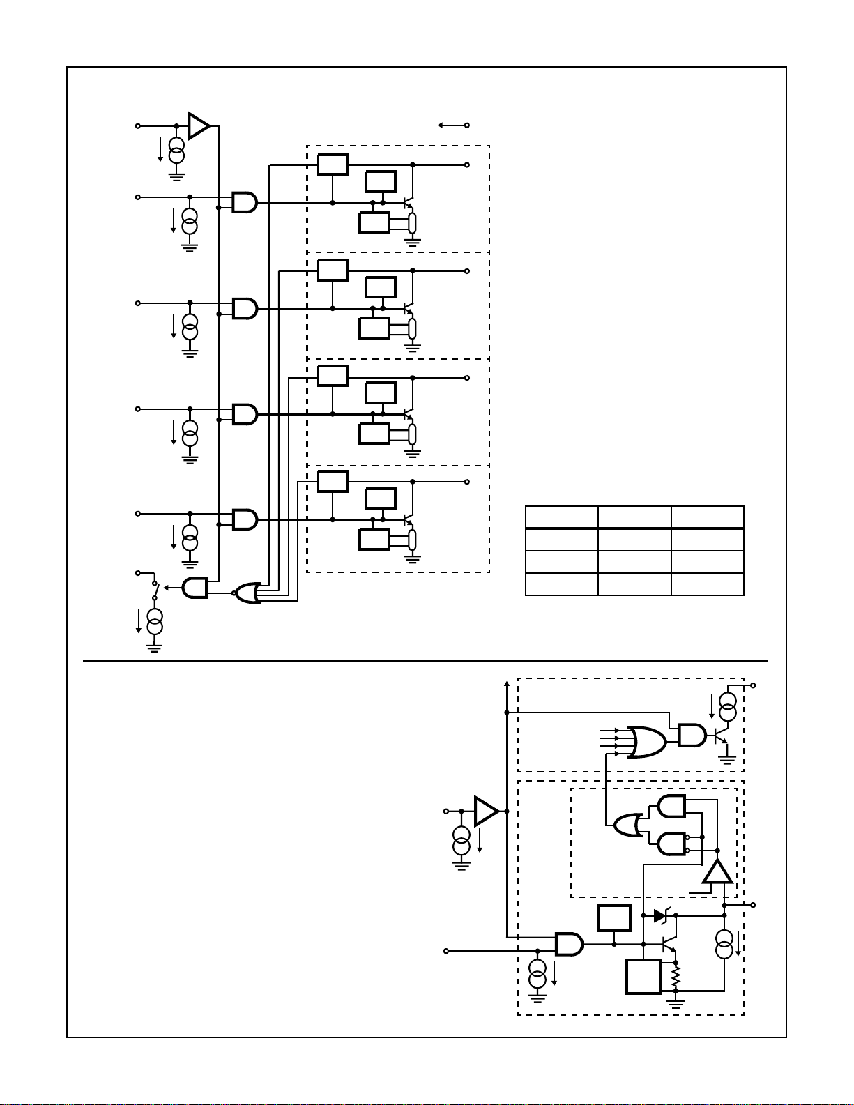
Block Diagram of the CA3272A
A
ENABLE
CA3272A, CA3292A
V
CC
IN D
IN C
IN B
IN A
FAULT
F
T
LIM
I
LIM
F
T
LIM
I
LIM
F
T
LIM
I
LIM
F
T
LIM
I
LIM
Q
D
0.02Ω
Q
C
0.02Ω
Q
B
0.02Ω
Q
A
0.02Ω
OUT D
OUT C
OUT B
OUT A
TRUTH TABLE
ENABLE IN OUT
HHL
HLH
LXH
H = High, L = Low, X = Don’t Care
Block Diagram of the CA3292A
(1 of 4 Outputs Shown with Expanded Fault Logic)
NOTE: The CA3292A is identical to the CA3272A except for the
collector-to-base Zener diode on each low side power output driver
(shown here as ZA). The Zener diode clamp is used as an overvoltage clamp to protect the output when switching inductive loads.
When the output voltage exceeds the Zener threshold, QA conducts
to suppress further increase in output voltage. The fault sense and
fault flag logic circuits are the same in the CA3272A and CA3292A.
ENABLE LINE
TO B, C AND D
INPUTS AND
FAULT OUTPUT
ENABLE
IN A
2
FAULT INPUT
FROM B, C, D
CHANNELS
CHANNEL A
1 OF 4
OUTPUTS
FAULT
FLAG LOGIC
FAULT SENSE
CHANNEL A
T
LIM
I
LIM
FAULT
Q
F
4V
Z
A
Q
A
0.02Ω
OUT
Page 3
CA3272A, CA3292A
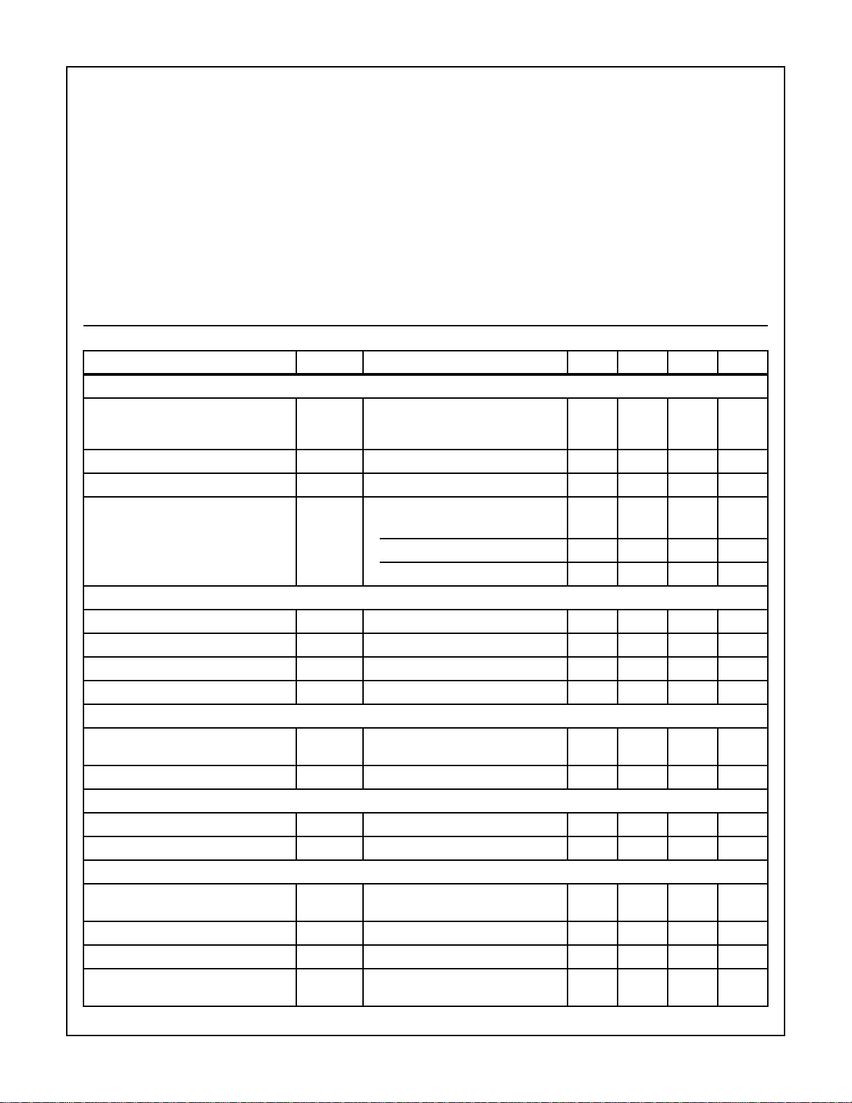
Absolute Maximum Ratings Thermal Information
Output Voltage, VO (CA3272A) . . . . . . . . . . . . . . . . . . . . . . . . +60V
Output Sustaining Voltage, V
Output Voltage, VO (CA3292A) . . . . . . . . . . . . . . . . . . . . . V
(CA3272A) . . . . . . . . . . . 40V
CE(SUS)
CLAMP
Maximum Output Clamp Energy (CA3292A) . . . . . . . . . . . (Note 8)
Output Transient Current, (Note 1) . . . . . . . . . . . . . . . . . . 1.6A Max.
Output Load Current, (Note 2) . . . . . . . . . . . . . . . . . . . . . . . . . .0.7A
Supply Voltage, VCC. . . . . . . . . . . . . . . . . . . . . . . . . . . . . . . . . . +7V
Logic Input Voltage, VIN . . . . . . . . . . . . . . . . . . . . . . . . . . . . . . 15V
FAULT Output Voltage, VF . . . . . . . . . . . . . . . . . . . . . . . . . . . . . 16V
Operating Conditions
Temperature Range . . . . . . . . . . . . . . . . . . . . . . . . . -40oC to 125oC
CAUTION: Stresses above those listed in “Absolute Maximum Ratings” may cause permanent damage to the device. This is a stress only rating and operation
of the device at these or any other conditions above those indicated in the operational sections of this specification is not implied.
Thermal Resistance (Typical, Note 3) θJA (oC/W)
For surface mount without added copper ground area:
CA3272AQ, CA3292AQ (PLCC) . . . . . . . . . . . . . . 45oC/W
CA3272AM, CA3292AM (SOIC). . . . . . . . . . . . . . . 56oC/W
For surface mount with 2 sq. in. of added copper ground area:
CA3272AQ, CA3292AQ (PLCC) . . . . . . . . . . . . . . 36oC/W
CA3272AM, CA3292AM (SOIC). . . . . . . . . . . . . . . 35oC/W
See Maximum Power Dissipation vs Temperature Curves,
Figures 6 and 7.
Maximum Junction Temperature (Plastic Packages) . . . . . . . 150oC
Maximum Storage Temperature Range . . . . . . . . . .-65oC to 150oC
Maximum Lead Temperature (Soldering 10s) . . . . . . . . . . . . . 300oC
(SOIC, PLCC - Lead Tips Only)
Electrical Specifications T
= -40oC to 125oC, VCC = 5.5V, Unless Otherwise Specified
A
PARAMETER SYMBOL TEST CONDITIONS MIN TYP MAX UNITS
OUTPUT PARAMETERS
Output (OFF) Current I
Output Sustaining Voltage: CA3272A V
Output Clamp Voltage: CA3292A V
Collector-to-Emitter Saturation Voltage V
LOGIC INPUT THRESHOLDS
Input Low Voltage V
Input High Voltage V
Input Low Current I
Input High Current I
SUPPLY CURRENT
All Outputs ON I
All Outputs OFF I
PROPAGATION DELAY
Turn-ON Delay t
Turn-OFF Delay t
FAULT PARAMETERS
Output Low Current, I
F(SINK)
(with Fault)
Output High Current, I
F(LK)
Output Low Voltage V
Output Driver Fault Sense, High
Threshold (Open)
CEX
VIN = 0.8V; VEN = 5.5V; (Note 4)
VCE = 60V for CA3272A
VCE = 24V for CA3292A
CE(SUS)
CLAMPIC
CE(SAT)VIN
CC(ON)VIN
CC(OFF)VIN
PHL
PLH
I
OL
Note 7 40 - - V
VCC = 3.5V - - 0.8 V
IL
IH
VIN = VEN = 0.8V; VCC = 4.75V 10 45 70 µA
IL
VIN = VEN = 5.5V 10 45 70 µA
IH
I
OUTC
I
LOAD
I
LOAD
VIN = 0.8V; VEN = 2.0V; VF = 4V
V
I
OH
V
HTHDVIN
No Fault (Note 5) - - 20 µA
External Load Equal Min. I
OL
- 30 100 µA
= 300µA; VEN = 0.8V 28 32 36 V
= 2V, VCC = 4.75V,
IC = 400mA, TA = 125oC - - 0.3 V
IC = 500mA, TA = 25oC - - 0.4 V
IC = 600mA, TA = -40oC - - 0.5 V
2--V
= VEN = 5.5V; I
= I
OUTD
= 400mA
OUTA
= I
OUTB
=
- - 65 mA
= 0V - - 10 mA
= 500mA - 3 10 µs
= 500mA - 3 10 µs
124mA
= Low = 1V; (Note 5)
OUT
OL
- 0.2 0.4 V
= 0.8V; VEN = 2V (Note 6) 3 4 5.5 V
3
Page 4

CA3272A, CA3292A
Electrical Specifications T
= -40oC to 125oC, VCC = 5.5V, Unless Otherwise Specified (Continued)
A
PARAMETER SYMBOL TEST CONDITIONS MIN TYP MAX UNITS
Output Driver Fault Sense, Low Threshold
V
LTHD
VIN = VEN = 2V (Note 6) 3 4 5.5 V
(Short)
PROTECTION PARAMETERS
Over-Current Limiting I
Over-Temperature Limiting
T
LIM
LIM
VIN = VEN = 2V, V
= 4Ω to 16V 0.7 - Note 1 A
OUT
- 165 -
(Junction Temperature)
Over-Temperature Limiting, Hysteresis T
HYS
-15-∆oC
DESIGN PARAMETERS
Input Capacitance C
Enable Capacitance C
IN
EN
-3-pF
- 4.6 - pF
NOTES:
1. Output Transient Currents are controlled by on-chip limiting for each output. Under short-circuit conditions with voltage applied to the
collector of the output transistor and with the output transistor turned ON, the current will increase to 1.2A, typical. Over-Current Limiting
protects a short circuit condition for a normal operating range of output supply voltage. During a short circuit condition, the output driver
will shortly thereafter (approximately 5ms) go into Over-Temperature Shutdown. While Over-Current Limiting may range to peak currents as high as 1.6A, each output will typically withstand a direct short circuit at normal single battery supply levels. Excessive dissipation before thermal shutdown occurs may cause damage to the chip for supply voltages greater than 16V. When sequentially
switched, the outputs are rated to withstand peak current, cold turn-on conditions of lamp loads such as #168 or #194 lamps.
2. The total DC current with all 4 outputs ON should not exceed the total of (4 x 0.7A + Max. ICC) ~ 2.85A. This level of current will significantly increase the chip temperature due to increased dissipation and may cause thermal shutdown in high ambient temperature conditions (See Absolute Maximum Ratings for Dissipation). Any one output may be allowed to exceed 0.7A but may be subject to OverCurrent Limiting above the I
the I
minimum limit of 0.7A. As a practical limit, no single output should be loaded to more than 1A maximum.
LIM
minimum limit of 0.7A. No single output should be loaded to more than Over-Current Limiting above
LIM
3. The PLCC and SOIC packages have power lead frame construction through the ground pins to conduct heat from the frame to the PC
Board ground area. Thermal resistance, θJA is given for a surface mount of the 28 lead PLCC and the 28 lead SOIC pac kages on a 1 oz.
copper PC board with minimal ground area and with a 2 square inches of ground area.
4. I
is the static leakage current at each output when that output is OFF (ENABLE Low). Refer to the Figure 3 illustration of an output
CEX
stage. The value of I
is both the leakage into the output driver and a pull-down current sink, I
CEX
. The purpose of the current
O(SINK)
sink is to detect open load conditions.
5. The IOL value of “Output Low Current, I
I
. The current sink is active only when a fault exists. When no fault exists, the IOH current at the FAULT pin is the maximum
F(SINK)
leakage current, I
. Refer to Figure 2 for an illustration of the FAULT output and associated external components. Refer to FAULT
F(LK)
” at the FAULT pin is both the static leakage of the output driver QF and the current sink,
F(SINK)
LOGIC TABLE for Fault Modes.
6. The Voltages, V
transitions for voltage forced at the outputs. V
V
indicates a shorted load when the output is increased greater than the threshold. The output voltage is changed until the FAULT
LTHD
HTHD
, V
are the comparator threshold reference values (Min. and Max. Range) sensed as a high and low state
LTHD
indicates an open load fault when the output is decreased to less than the threshold.
HTHD
pin indicates a Low (Fault). Refer to Figure 2 for test value of external resistor. Refer to IOL and IOH FAULT PARAMETERS Test Limits
to determine VOL and VOH at the FAULT pin.
7. Tested with 120mA switched off in a Load of 70mH and 32Ω series resistance;
CA3272A: Outputs clamped with an external Zener diode, limiting V
CA3292A: Outputs limited to the V
voltage by the internal collector-to-base Zener diode and output transistor clamp.
CLAMP
OUT
to the V
maximum rating of +40V.
CE(SUS)
8. The single pulse clamp energy rating for the CA3292A is defined over a range of operating conditions. The Clamp Energy is a function
of the Load Inductance, Load Resistance, Clamp Voltage, Supply Voltage, the Saturated ON Resistance (V
) and the Steady State
SAT
Load Current at the instant of Turn-OFF. Refer to Figure 5 for the Safe Operating Area when driving inductive loads. Rating limits for
Energy vs Single Pulse Width Time are plotted for different coil values. Refer to Application Note - AN9416 for pulse energy calculation
methods.
o
C
4
Page 5

Applications
CA3272A, CA3292A
The CA3272A and CA3292A are quad-gated inverting lowside power drivers with a fault diagnostic flag output. Both
circuits are rated for 125
o
C ambient temperature applications and have current limiting and thermal shutdown. While
functionally similar to the CA3262AQ, they differ in the mode
of over-voltage protection and have the added feature of a
FAULT flag output. Also, as shown in Figure 1, the inputs to
channels A, B, C, D and ENABLE have internal pulldowns to
turn “OFF” the outputs when the inputs are floating.
V
CC
CONSTANT
CURRENT SOURCE
INPUT
ENABLE
FIGURE 1. SCHEMATIC OF ONE INPUT STAGE
REFERENCE
1.2 VOLTS
TO PREDRIVER
AND
OUTPUT STAGES
As noted in the Block Diagrams, the CA3292A is equivalent
to the CA3272A except that it has internal clamp diodes on
the outputs to handle inductive switching pulses from the
output load. The structure of each CA3292A output includes
a Zener diode from collector-to-base of the output transistor.
This is a different form of protection from other quad drivers
with current steering clamp diodes on each output, paired to
one of two “CLAMP” output pins. The CA3292A output transistor will turn-on at the Zener diode clamp voltage threshold
which is typically 32V and the output transistor will dump the
pulse energy through the output driver to ground.
Each output driver is capable of switching 600mA load currents
and operate at 125
o
C ambient temperature without interaction
between the outputs. The CA3272A and CA3292A can drive
four incandescent lamp loads without modulating their brilliance
when the “cold” lamps are energized. The outputs can be connected in parallel to drive larger loads. Over-current or short circuit output load conditions are fault protected by current limiting
with a typical limit value of 1.2A. The current limiting range is
set for 0.6A to 1.6A. The output stage does not change state
(oscillate) when in the current limit mode.
FAULT LOGIC TABLE
IN OUT FAULT MODE
H L H Normal
H H L Over Current, Over T emper ature Open
LL L
L H H Normal
Load or Short to Power Supply
Any one output that faults (see F ault Logic Table) will switch the
F AULT output at pin 1 to a constant current pull-down.
The Fault Logic circuit, as shown in the Block Diagram for
the CA3292A, applies to both the CA3272A and CA3292A.
The Fault Sense circuits do not override or control the power
switching circuits of the IC. Their primary function is to provide an external diagnostic fault flag output. Each Power
Switching Channel has diagnostic fault sensing input to the
Fault Logic. The Fault Logic block of the functional Block Diagram illustrates the logic functions associated with Fault
detection. The diagnostic output for each of the four channels
of switching is processed through the fault logic circuit associated with each channel. It is then passed to an OR gate
which controls the FAULT flag output transistor, Q
thru A 2
F
input AND gate.
ENABLE IN
B, C AND D
FAULT MODE
INPUTS
FAULT MODE
INPUT
CHANNEL “A”
FIGURE 2. EXTERNAL FAULT OUTPUT CIRCUIT AND I
AS FAULT SINK PULLDOWN CURRENT, WHICH IS
ACTIVATED BY TRANSISTOR, QF, WHEN A FAULT
EXISTS
I
F(SINK)
Q
F
1
FAULT
LOGIC
OUTPUT
TX = RXC
VCC = +5V
R
X
FAULT FLAG
DIAGNOSTIC
OUTPUT, V
C
X
≈ 0.5 TO 1ms
X
F
F(SINK)
The ENABLE input is common to each of the 4 power
switches and also disables the FAULT flag output at the
2 input AND gate when it is low. The Fault Logic circuit
senses the IN and OUT states and switches Q
fault is detected. Transistor Q
activates a sink current
F
“ON” if a
F
source to pull-down the FAULT pin to a 0 (low) state when
the fault is detected. Both shorted and open load conditions
are detected.
It is normal for thermal shutdown and current limiting to
occur sequentially during a short circuit fault condition. A
precaution applies for potential damage from high transient
dissipation during thermal shutdown. (See Note 1 following
the Electrical Specifications Table).
Each of the outputs are independently protected with overcurrent limiting and over-temperature shutdown with thermal
hysteresis. If an output is shorted, the remaining outputs
function normally unless the temperature rise of the other
output devices can be made to exceed their shutdown temperature of 165
a driver exceeds the 165
o
C typical. When the junction temperature of
o
C thermal shutdown value, that
output is turned off. When an output is shutdown, the resulting decrease in power dissipation allows the junction temperature to decrease. When the junction temperature
decreases by approximately 15
o
C, the output is turned on.
5
Page 6

CA3272A, CA3292A
The output will continue to turn on and off for as long as the
shorted condition exists or until shutdown by the input logic.
The resulting frequency and duty cycle of the output current
flow is determined by the ambient temperature, the thermal
resistance of the package in the application and the total
power dissipation in the package. Since each output is independently protected, the frequency and duty cycle of the current flow into multiple shorted outputs will not be related in
time. Long lead lengths in the load circuit may lead to oscillatory behavior if more than two output loads are shorted.
V
FAULT SENSE
THRESHOLD, V
4V
ZENER
CLAMP
Z
T
LIM
FIGURE 3. OUTPUT OPEN LOAD DETECTION WHERE I
IS AN ACTIVE CURRENT SINK PULLDO WN FOR
OPEN-LOAD FAULT DETECTION. THE CURRENT
I
IS I
CEX
O(SINK)
THE OUTPUT DRIVER
A
Q
A
I
LIM
PLUS LEAKAGE CURRENTS OF
0.02Ω
THD
BATT
2
OUT A
I
O(SINK)
R
LOAD
O(SINK)
Since a diagnostic flag indicates when an output is shorted,
this information can be used as input to a microprocessor or
dedicated logic circuit to provide a fast switch-off when a
short occurs and, by sequence action, can be used to determine which output is shorted. A fault condition in any output
load will cause the FAULT output to switch to a logic “low”.
Since a fault condition may be detected during switching,
use of an appropriate size capacitor to filter the FAULT output is recommended. The recommended FAULT output circuit is shown in Figure 2. This will prevent the FAULT output
voltage from reaching a logic level “0” within the maximum
switching time.
The FAULT detection circuitry compares the state of the
input and the state of the output for each A, B, C and D
channel. The output is considered to be in a high state if the
voltage exceeds the typical FAULT threshold reference voltage, V
of 4V. If the output voltage is less than V
THD
THD
, the
output is considered to be in a low state. For example, if the
input is high and the output is less than V
, a normal
THD
“ON” condition exists and the FAULT output is high. If the
input is high and the output is greater than V
, a shorted
THD
load condition is indicated and the FAULT output is low.
When the input is low and the output is greater than V
THD
, a
normal “OFF” condition is indicated and the FAULT output is
high. If the input is low and the output is less than V
THD
, an
open load condition exists and the FAULT output is low. The
Output Driver Fault Sense state is determined by high and
low comparator threshold limits which are defined in the
Fault Parameters section of the Electrical Specifications.
The FAULT output diagram of Figure 2 shows the circuit
component interface for sensing a diagnostic fault condition.
As noted, the time constant of T
= RXCX should be greater
X
than the ON-OFF output switching times to avoid false fault
readings during switching. For applications requiring fast
period repetition rates, the maximum time constant should
be significantly less than the period of switching. The shortest practical time constant is preferred to limit the duration of
a fault condition.
To match a standard CMOS or TTL interface, the switched
current at the FAULT pin must be converted to V
and V
IH
voltage levels using the RX external pullup resistor. The minimum specified I
(Fault) state which is used to test for a V
0.4V. This makes the calculation for the V
tively simple. Where V
the power supply voltage, R
limit at the F AULT output defines the Low
OL
is the FAULT output voltage, VCC is
F
is the pullup resistor to V
X
maximum limit of
OL
input level rela-
IL
CC
from the FAULT pin and IOL is the fault condition sink current, I
O(SINK)
VF = VCC - RXIOL≤ V
, the low state equation is:
IL
(EQ. 1)
As an example: Since TTL is the worst case for a low state,
V
= 0.8V. Using VCC = 5V, maximum VF = VOL = 0.4V and
IL
minimum I
worst case limit, the minimum value of R
RX = (VCC - VIL)/IOL = (5 - 0.4)V/0.001mA = 4.6kΩ
= 1mA for the CA3272A and CA3292A. At the
OL
is:
X
The preferred value for RX would be greater than the values
calculated.
For the logic V
VF = VCC - RXIOH≥ V
High (normal state),
IH
IH
(EQ. 2)
Where the IOH current is the specified leakage current,
I
at the FAULT pin, it remains to check the calculated
F(LK)
value for R
resistance. To determine that the minimum V
FAULT pin is greater than V
as a leakage current times the chosen pullup
X
to an external logic match, V
IH
from the
OH
is calculated using Equation 2. For example, using the minimum R
VF = [5 - (4.6kΩ x 20µA)] = 4.9V
resistor value calculated for the CA3272A,
X
which is more than suitable for CMOS or TTL Input s witching
levels; suggesting that a larger value of R
(such as 10kΩ)
X
could be used for a better noise margin in the Low f ault state.
To detect an open load, each output has an inter nal low-level
current sink, shown in Figure 3, which acts as a pull-down
under open load fault conditions and is alwa ys active . The magnitude of this current plus any leakage associated with the output transistor will always be less than 100µA. (The data sheet
specification for I
includes this internal low-level sink cur-
CEX
rent). The output load resistance must be chosen such that the
voltage at the output will not be less than V
when the I
THD
CEX
sink current flows through it under worse case conditions with
minimum supply voltage. For example, assume a 6.5V minimum driver output supply voltage, a FAULT threshold reference
voltage of V
I
= 100µA. Calculate the maximum load resistance that will
CEX
= 5.5V and an output current sink of
THD
not result in a F AULT output low state when the output is OFF.
IL
F
6
Page 7

CA3272A, CA3292A
R
(max) = [V
LOAD
R
(max) = (6.5V - 5.5V) / 100µA = 10kΩ (EQ. 4)
LOAD
Since the CA3272A do not have on-chip diodes to clamp
voltage spikes which may be generated during inductive
switching of the load circuit, an external Zener diode (30V or
less is recommended) should be connected between the
output terminal and ground. Only those outputs used to
switch inductive loads require this protection. Note that since
the rate of change of output current is very high, even small
values of inductance can generate voltage spikes of considerable amplitude on the output terminals which may require
clamping. External free-wheeling diodes returned to the supply voltage are generally not acceptable as inductive clamps
if the supply voltage exceeds 30V during transients. Typical
loads for either the CA3272A or CA3292A are shown in the
application circuit of Figure 4A. Where inductive loads are
driven from outputs A and B, no external Zener diode clamp
is needed for the CA3292A but is required for the CA3272A
as shown in Figure 4B.
SUPPLY
(min) - V
THD
(max)] / I
(max) (EQ. 3)
CEX
The CA3272A and CA3292A are supplied in specially configured power packages to conduct heat from the junction
through the mounting structure and device leads to the PC
Board. The ground leads are directly connected to the
mounting pad of the chip. The junction-to-air thermal resistance, θ
may be significantly improved by suitable layout
JA
design of the PC board to which the package is soldered.
Two or more square inches of PC Board ground area next to
the device ground pins is recommended. The PC Board
ground layer should be on the device side of the board with
open space for heat radiation.
Refer to Application Note AN9416 for additional thermal
information. Further information is provided on pulse energy
calculation methods for inductive load applications with
detail explaining the Safe Operating Area shown in Figure 5.
The SOA area for single energy transients is below the dotted lines for the given ambient temperature conditions. The
energy locus plots of the three inductive coils were made for
arbitrarily chosen values of inductance and are shown here
for reference information. The RL time constant, ambient
temperature, clamp voltage and the stored energy in the coil
determine the SOA limits.
FAULT
FAULT
FAULT
FAULT
CA3292A
OUT A
Z
I
I
I
I
LIM
LIM
LIM
LIM
A
Q
A
OUT B
Z
B
Q
B
OUT C
Z
C
Q
C
OUT D
Z
D
Q
D
T
LIM
T
LIM
T
LIM
T
LIM
RELAY
LAMP
+V
BATT
SOLENOID
+V
BATT
HIGH CURRENT
HIGH SIDE DR
MOTOR
+V
BATT
INDUCTIVE
FAULT
T
LIM
I
LIM
CA3272A
(1 OF 4 CHANNELS)
EXTERNAL ZENER DIODE CLAMP
PROTECTION FROM POSITIVE VOLTAGE
SPIKE (INDUCTIVE KICK PULSE) AT TURN-OFF
OUT A
Q
A
LOAD
+V
BATT
V
Z(EXT)
NOTE: The internal drive circuit with self protection and fault output
is the CA3292A with the over voltage Zener diode clamp.
FIGURE 4A. TYPICAL APPLICATION CIRCUIT SHOWING OUT-
PUT LOAD CONTROL CAPABILITY OF THE
CA3272A OR CA3292A
NOTE: The V
voltage rating is the maximum voltage for full
CE(SUS)
load switching.
FIGURE 4B. CA3272A OVER-VOLTAGE PROTECTION IS AN
EXTERNAL ZENER DIODE CLAMP WHERE
V
≤ V
Z(EXT)
CE(SUS)
7
Page 8

CA3272A, CA3292A
200
550mH COIL - LINE 1
265mH COIL - LINE 2
136mH COIL - LINE 3
100
DO NOT
OPERATE ABOVE
THE DOTTED
LINES
50
SINGLE PULSE ENERGY (mJ)
10
110100
2
3
SINGLE PULSE TIME (ms)
FIGURE 5. CA3292A SINGLE PULSE INDUCTIVE FLYBACK CLAMP ENERGY SOA RATING CHART FOR EACH OUTPUT DRIVER
25oC MAX LIMIT
V
CLAMP
1
V
SAFE OPERATING
AREA - BELOW
DOTTED LINES
= VZ+V
Z
OUT x
Q
X
BE
L
125oC MAX
LIMIT
V
BATT
R
2.0
1.5
1
0.5
PACKAGE DISSIPATION (W)
0
-50oC0
o
C50
AMBIENT TEMPERATURE (
SOIC
PLCC
o
C 100oC 150oC
ο
C)
FIGURE 6. MAXIMUM POWER DISSIP ATION RATING vs
TEMPERATURE FOR THE CA3272AQ, CA3292AQ
PLCC P A CKA GE AND THE CA3272AM, CA3292AM
SOIC PACKAGE WITH NO ADDITIONAL PC
BOARD AREA FOR HEAT SINKINGS
2.0
1.5
1
0.5
PACKAGE DISSIPATION (W)
0
-50oC0
o
C50
AMBIENT TEMPERATURE (οC)
o
C 100oC
SOIC/PLCC
FIGURE 7. MAXIMUM POWER DISSIP ATION RATING vs
TEMPERATURE FOR THE CA3272AQ, CA3292AQ
PLCC P A CKA GE AND THE CA3272AM, CA3292AM
SOIC PACKA GE WITH 2 SQ. IN. OF 1 OZ. COPPER
PC BOARD AREA FOR HEAT SINKING
150oC
8
Page 9

CA3272A, CA3292A
Small Outline Plastic Packages (SOIC)
N
INDEX
AREA
123
-A-
0.25(0.010) B
E
SEATING PLANE
D
-C-
H
-B-
A
M
L
h x 45
M
o
α
e
B
0.25(0.010) C AMB
M
NOTES:
1. Symbols are defined in the “MO Series Symbol List” in Section
2.2 of Publication Number 95.
2. Dimensioning and tolerancing per ANSI Y14.5M-1982.
3. Dimension “D” does not include mold flash, protrusions or gate
burrs. Mold flash, protrusion and gate burrs shall not exceed
0.15mm (0.006 inch) per side.
4. Dimension “E” does not include interlead flash or protrusions. Interlead flash and protrusions shall not exceed 0.25mm (0.010
inch) per side.
5. The chamfer on the body is optional. If it is not present, a visual
index feature must be located within the crosshatched area.
6. “L” is the length of terminal for soldering to a substrate.
7. “N” is the number of terminal positions.
8. Terminal numbers are shown for reference only.
9. The lead width “B”, as measured 0.36mm (0.014 inch) or greater
above the seating plane, shall not exceed a maximum value of
0.61mm (0.024 inch)
10. Controlling dimension: MILLIMETER. Converted inch dimensions are not necessarily exact.
A1
0.10(0.004)
S
M28.3 (JEDEC MS-013-AE ISSUE C)
28 LEAD WIDE BODY SMALL OUTLINE PLASTIC PACKAGE
INCHES MILLIMETERS
SYMBOL
A 0.0926 0.1043 2.35 2.65 -
A1 0.0040 0.0118 0.10 0.30 -
B 0.013 0.0200 0.33 0.51 9
C 0.0091 0.0125 0.23 0.32 D 0.6969 0.7125 17.70 18.10 3
E 0.2914 0.2992 7.40 7.60 4
e 0.05 BSC 1.27 BSC H 0.394 0.419 10.00 10.65 -
C
h 0.01 0.029 0.25 0.75 5
L 0.016 0.050 0.40 1.27 6
N28 287
o
α
0
o
8
o
0
o
8
Rev. 0 12/93
NOTESMIN MAX MIN MAX
-
9
Page 10

CA3272A, CA3292A
Plastic Leaded Chip Carrier Packages (PLCC)
0.042 (1.07)
0.048 (1.22)
PIN (1) IDENTIFIER
0.020 (0.51) MAX
3 PLCS
C
L
D1
D
0.026 (0.66)
0.032 (0.81)
0.050 (1.27) TP
0.042 (1.07)
0.056 (1.42)
C
L
E1
E
0.013 (0.33)
0.021 (0.53)
0.004 (0.10) C
0.025 (0.64)
0.045 (1.14)
D2/E2
D2/E2
A1
A
-C-
VIEW “A”
0.020 (0.51)
MIN
SEATING
PLANE
R
N28.45 (JEDEC MS-018AB ISSUE A)
28 LEAD PLASTIC LEADED CHIP CARRIER PACKAGE
INCHES MILLIMETERS
SYMBOL
A 0.165 0.180 4.20 4.57 -
A1 0.090 0.120 2.29 3.04 -
D 0.485 0.495 12.32 12.57 D1 0.450 0.456 11.43 11.58 3
D2 0.191 0.219 4.86 5.56 4, 5
E 0.485 0.495 12.32 12.57 E1 0.450 0.456 11.43 11.58 3
E2 0.191 0.219 4.86 5.56 4, 5
N28 286
NOTESMIN MAX MIN MAX
Rev. 1 3/95
0.045 (1.14)
MIN
VIEW “A” TYP.
0.025 (0.64)
MIN
NOTES:
1. Controlling dimension: INCH. Converted millimeter dimensions
are not necessarily exact.
2. Dimensions and tolerancing per ANSI Y14.5M-1982.
3. Dimensions D1 and E1 do not include mold protrusions. Allowable mold protrusion is 0.010 inch (0.25mm) per side.
4. To be measured at seating plane contact point.
-C-
5. Centerline to be determined where center leads exit plastic body.
6. “N” is the number of terminal positions.
All Intersil semiconductor products are manufactured, assembled and tested under ISO9000 quality systems certification.
Intersil products are sold by description only. Intersil Corporation reserves the right to make changes in circuit design and/or specifications at any time without
notice. Accordingly, the reader is cautioned to verify that data sheets are current before placing orders. Information furnished by Intersil is believed to be accurate
and reliable. However, no responsibility is assumed by Intersil or its subsidiaries for its use; nor for any infringements of patents or other rights of third parties which
may result from its use. No license is granted by implication or otherwise under an y patent or patent rights of Intersil or its subsidiaries.
For information regarding Intersil Corporation and its products, see web site http://www.intersil.com
10
 Loading...