

Page 1

CA3280, CA3280A
Data Sheet September 1998 File Number 1174.4
Dual, 9MHz, Operational
Transconductance Amplifier (OTA)
The CA3280 and CA3280A types consist of two variable
operational amplifiers that are designed to substantially reduce
the initial input offset voltage and the offset voltage v ariation
with respect to changes in programming current. This design
results in reduced“AGCthump,”an objectionable characteristic
of many AGC systems. Interdigitation, or crosscoupling, of
critical portions of the circuit reduces the amplifier dependence
upon thermal and processing variables.
The CA3280 has all the generic characteristics of an
operational voltage amplifier except that the forward transfer
characteristics is best described by transconductance rather
than voltage gain, and the output is current, not voltage. The
magnitude of the output current is equal to the product of
transconductance and the input voltage. This type of
operational transconductance amplifier was first introduced in
1969, and it has since gained wide acceptance as a gateable,
gain controlled building block f or instrumentation and audio
applications, such as linearization of transducer outputs,
standardization of widely changing signals for data processing,
multiplexing, instrumentation amplifiers operating from the
nanopower range to high current and high speed comparators.
For additional application information on this device and on
OTAs in general, please refer to Application Notes: AN6818,
AN6668, and AN6077.
Pinout
CA3280
(PDIP, CERDIP)
TOP VIEW
Features
• Low Initial Input Offset Voltage: 500µV (Max) (CA3280A)
• Low Offset Voltage Change vs I
: <500µV (Typ)
ABC
for All Types
• Low Offset Voltage Drift: 5µV/
o
C (Max) (CA3280A)
• Excellent Matching of the Two Amplifiers for All
Characteristics
• Internal Current-Driven Linearizing Diodes Reduce the
External Input Current to an Offset Component
• Flexible Supply Voltage Range. . . . . . . . . . . ±2V to ±15V
Applications
• Voltage Controlled Amplifiers
• Voltage Controlled Oscillators
• Multipliers
• Demodulators
• Sample and Hold
• Instrumentation Amplifiers
• Function Generators
• Triangle Wave-to-Sine Wave Converters
• Comparators
• Audio Preamplifier
Ordering Information
PART NUMBER
TEMP.
RANGE (oC) PACKAGE
PKG.
NO.
ID, A1
EMITTER, A1
, A1
I
ABC
NC
, A2
I
ABC
EMITTER, A2
ID, A2
+IN, A1
1
A1
2
3
4
V-
5
6
7
A2
8
16
+
-
15
-IN, A1
V+, A1
14
13
OUT, A1
OUT, A2
12
V+, A2
11
-IN, A2
10
-
+
9
+IN, A2
1
CAUTION: These devices are sensitive to electrostatic discharge; follow proper IC Handling Procedures.
CA3280AE -55 to 125 16 Ld PDIP E16.3
CA3280E 0 to 70 16 Ld PDIP E16.3
CA3280AF3 -55 to 125 16 Ld CERDIP F16.3
1-888-INTERSIL or 321-724-7143
| Copyright © Intersil Corporation 1999
Page 2

.Functional Diagram
CA3280, CA3280A
1/2 CA3280
-
15
10
+
16
9
1
8
2K 2K
6
3
14
11
7
2
13
12
4
2
Page 3
CA3280, CA3280A
Absolute Maximum Ratings Thermal Information
Supply Voltage (Between V+ and V-). . . . . . . . . . . . . . . . . . . . +36V
Differential Input Voltage . . . . . . . . . . . . . . . . . . . . . . . . . . . . . . . 5V
Input Voltage Range . . . . . . . . . . . . . . . . . . . . . . . . . . . . . . V+ to V-
Input Current at ID = 0 . . . . . . . . . . . . . . . . . . . . . . . . . . . . . . 100µA
Amplifier Bias Current (I
). . . . . . . . . . . . . . . . . . . . . . . . . . 10mA
ABC
Output Short Circuit Duration (Note 1). . . . . . . . . . . . . . . . Indefinite
Linearizing Diode Bias Current, ID. . . . . . . . . . . . . . . . . . . . . . . 5mA
Peak Input Current with Linearizing Diode. . . . . . . . . . . . . . . . . . ±I
D
Operating Conditions
Temperature Range
CA3280 . . . . . . . . . . . . . . . . . . . . . . . . . . . . . . . . . . 0oC to 70oC
CA3280A . . . . . . . . . . . . . . . . . . . . . . . . . . . . . . . -55oC to 125oC
Supply Voltage Range (Typ) . . . . . . . . . . . . . . . . . . . . .±2V to ±15V
CAUTION: Stresses above those listed in “Absolute Maximum Ratings” may cause permanent damage to the device. This is a stress only rating and operation of the
device at these or any other conditions above those indicated in the operational sections of this specification is not implied.
NOTES:
1. Short circuit may be applied to ground or to either supply.
2. θJA is measured with the component mounted on an evaluation PC board in free air.
Thermal Resistance (Typical, Note 2) θJA (oC/W) θJC (oC/W)
CERDIP Package. . . . . . . . . . . . . . . . . 65 16
PDIP Package . . . . . . . . . . . . . . . . . . . 100 N/A
Maximum Junction Temperature (CERDIP P a ckage). . . . . . . . .175oC
Maximum Junction Temperature (Plastic Package) . . . . . . . .150oC
Maximum Storage Temperature Range. . . . . . . . . . -65oC to 150oC
Maximum Lead Temperature (Soldering 10s) . . . . . . . . . . . . 300oC
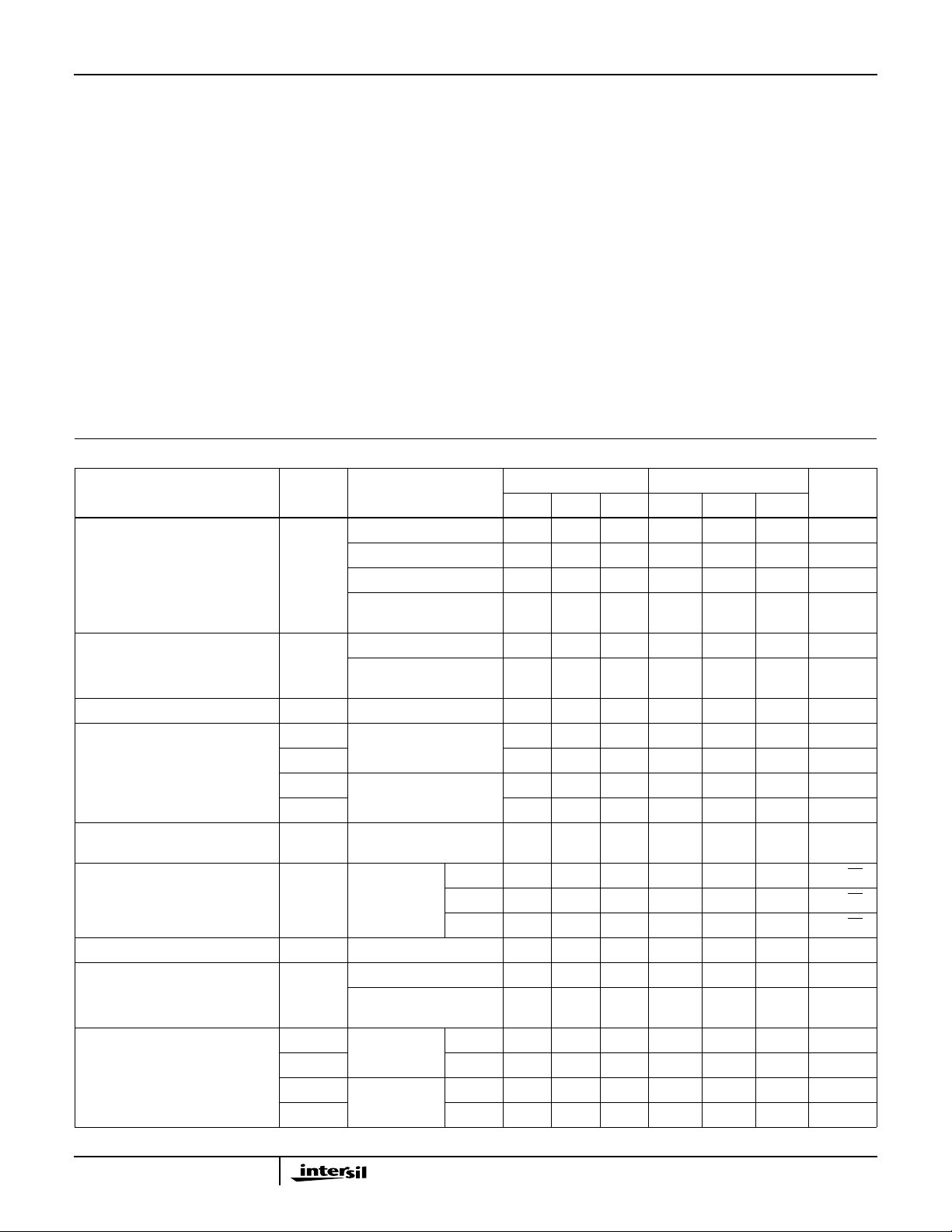
Electrical Specifications For Equipment Design, at T
P ARAMETER SYMBOL TEST CONDITIONS
Input Offset Voltage V
Input Offset Voltage Drift |∆VIO|I
Amplifier Bias Voltage V
Peak Output Voltage VOM+I
VOM- 12 -14.3 - -13.3 -14.3 - V
VOM+I
VOM- 12 -14.5 - -13.5 -14.5 - V
Common Mode Input Voltage
V
Range
Noise Voltage e
Input Offset Current I
Input Bias Current I
Peak Output Current IOM+I
IOM- Sink -350 -410 -650 -350 -410 -650 µA
IOM+I
IOM- Sink -3 -4.1 -7 -3 -4.1 -7 µA
I
IO
ABC
I
ABC
I
ABC
I
ABC
TA= Full Temp. Range
ABC
I
ABC
Temperature Range
ABCIABC
ABC
ABC
ICRIABC
I
N
ABC
I
IO
ABC
I
IB
ABC
I
ABC
Temperature Range
ABC
ABC
= 1mA - - 3 - - 0.5 mV
= 100µA - 0.7 3 - 0.25 0.5 mV
= 10µA - - 3 - - 0.5 mV
= 1mA to 10µA,
= 1µA to 1mA - 0.5 1 - 0.5 1 mV
= 100µA, TA = Full
= 100µA - 1.2 - - 1.2 - V
= 500mA 12 13.7 - 12.5 13.7 - V
= 5µA 12 13.9 - 12.5 13.9 - V
= 100µA -13 - 13 -13 - 13 V
= 500µA 10Hz - 20 - - 20 - nV/√Hz
= 500µA -Z 0.3 0.7 - 0.3 0.7 µA
= 500µA - 1.8 5 - 1.8 5 µA
= 500µA, TA = Full
= 500µA Source 350 410 650 350 410 650 µA
= 5µA Source 3 4.1 7 3 4.1 7 µA
= 25oC, V
A
= ±15V, Unless Otherwise Specified
SUPPLY
CA3280 CA3280A
- 0.8 4 - 0.8 1.5 mV
-5- - 3 5µV/oC
1kHz - 8 - - 8 - nV/√Hz
10kHz - 7 - - 7 - nV/√Hz
-38- 3 8 µA
UNITSMIN TYP MAX MIN TYP MAX
3
Page 4
CA3280, CA3280A
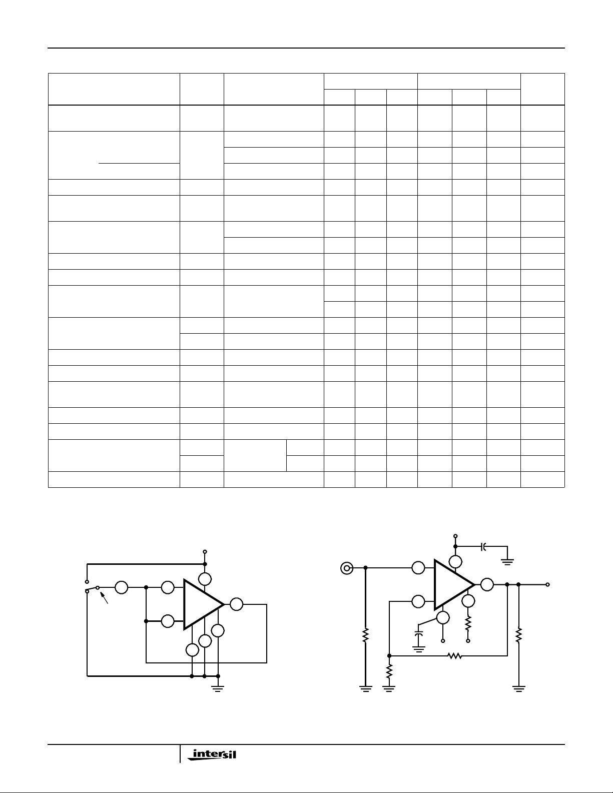
Electrical Specifications For Equipment Design, at T
= 25oC, V
A
= ±15V, Unless Otherwise Specified (Continued)
SUPPLY
CA3280 CA3280A
P ARAMETER SYMBOL TEST CONDITIONS
Peak Output Current Sink and
Source
IOM-,
IOM+
I
= 500µA, TA = Full
ABC
Temperature Range
350 450 550 350 450 550 µA
UNITSMIN TYP MAX MIN TYP MAX
Linearization Diodes ID = 100µA - 10 - - 10 - µA
Offset Current ID = 10µA - 0.5 1 - 0.5 1 µA
Dynamic Impedance ID = 100µA - 700 - - 700 - Ω
Diode Network Supply Current I
Amplifier Supply Current
I+ I
= 100µA 250 400 800 250 400 800 µA
ABC
= 500µA - 2 2.4 - 2 2.4 mA
ABC
(Per Amplifier)
Amplifier Output Leakage Current I
Common Mode Rejection Ratio CMRR I
Power Supply Rejection Ratio PSRR I
Open Loop Voltage Gain A
Forward Transconductance G
Input Resistance R
OL
g
OL
M
M
I
I
= 0, VO = 0V - 0.015 0.1 - 0.015 0.1 nA
ABC
I
= 0, VO = 30V - 0.15 1 - 0.15 1 nA
ABC
= 100µA 80 100 - 94 100 - dB
ABC
= 100µA 86 105 - 94 105 - dB
ABC
I
= 100µA,
ABC
RL = ∞, VO = 20V
I
=50µA, Large Signal - 0.8 1.2 - 0.8 1.2 mS
ABC
I
= 1mA, Small Signal - 16 22 - 16 22 mS
ABC
I
= 10µA 0.5 - - 0.5 - - MΩ
ABC
P-P
94 100 - 94 100 - dB
50 100 - 50 100 - kV/V
Channel Separation f = 1kHz - 94 - - 94 - dB
Open Loop Total
Harmonic Distortion
Bandwidth f
Slew Rate, Open Loop SR I
Capacitance C
Output Resistance R
THD f = 1kHz, I
RL = 15kΩ, VO = 20V
I
T
I
C
O
O
= 1mA, RL = 100Ω - 9 - - 9 - MHz
ABC
= 1mA - 125 - - 125 - V/µs
ABC
I
= 100µA Input - 4.5 - - 4.5 - pF
ABC
I
= 100µA - 63 - - 63 - MΩ
ABC
ABC
= 1.5mA,
P-P
- 0.4 - - 0.4 - %
Output - 7.5 - - 7.5 - pF
Test Circuits and Waveforms
14
+
1/2
CA3280
-
4
30kΩ
V+
0.1µF
3
30kΩ
+30V
INPUT
16
30V
0V
TEST
POINT
I
15
16
14
-
1/2
CA3280
+
1
3
1kΩ
0.1
µF
15
13
4
1kΩ
FIGURE 1. LEAKAGE CURRENT TEST CIRCUIT FIGURE 2. CHANNEL SEPARATION TEST CIRCUIT
4
13
V+V-
OUTPUT
10kΩ
Page 5

CA3280, CA3280A
Test Circuits and Waveforms (Continued)
V+
15V
14
10kΩ
10kΩ
FIGURE 3A. EFFECTS OF DIODE LINEARIZATION, WITH DIODE PROGRAMMING TERMINAL ACTIVE
10kΩ
10kΩ
16
15
I
9
10
I
DIODE
1/2
CA3280
1
DIODE
1/2
CA3280
I
8
3
ABC
V-
-15V
13
4
V-
-15V
V+
15V
11
6
4
I
ABC
1kΩ
12
1kΩ
I
OUT
I
OUT
V
IN
I
= 650µA, ID = 200µA; Vertical = 200µA/Div.;
ABC
Horizontal = 1V/Div.
V
IN
I
= 650µA; ID = 0; Vertical = 200µA/Div.;
ABC
Horizontal = 25mV/Div.
FIGURE 3B. WITH DIODE PROGRAMMING TERMINAL CUTOFF
FIGURE 3. CA3280 TRANSFER CHARACTERISTICS
Application Information
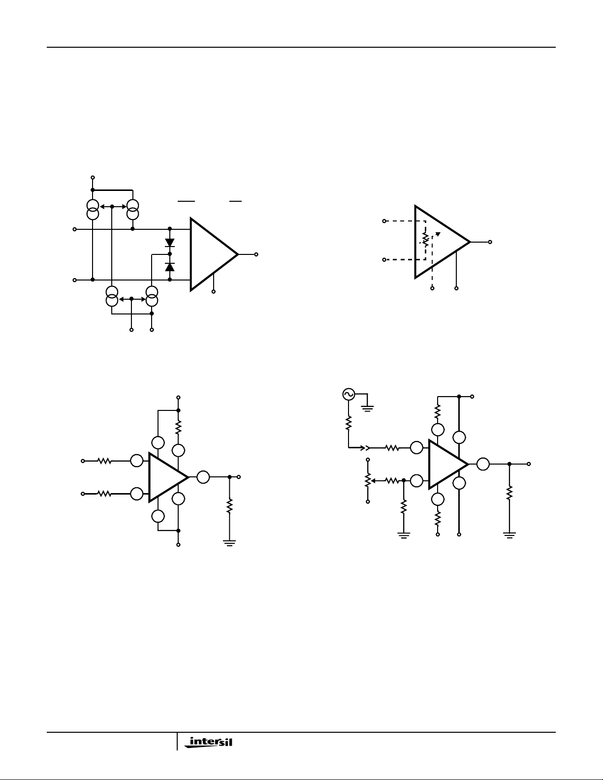
Figures 4 and 5 show the equivalent circuits for the current
source and linearization diodes in the CA3280. The current
through the linearization network is approximately equal to the
programming current. There are sev eral adv antages to driving
these diodes with a current source. First, only the offset current
from the biasing network flows through the input resistor.
Second, another input is provided to extend the gain control
dynamic range. And third, the input is truly differential and can
accept signals within the common mode range of the CA3280.
Typical Applications
The structure of the variable operational amplifier eliminates
the need for matched resistor networks in differential to single
ended converters, as shown in Figure 6. A matched resistor
5
network requires ratio matching of 0.01% or trimming for 80dB
of common-mode rejection. The CA3280, with its excellent
common mode rejection ratio, is capable of converting a small
(±25mV) differential input signal to a single-ended output
without the need for a matched resistor network.
Figure 7 shows the CA3280 in a typical gain control application.
Gain control can be performed with the amplifier bias current
(l
). With no diode bias current, the gain is merely gMRL.For
ABC
example, with an l
of 1mA, the gM is approximately 16mS.
ABC
With the CA3280 operating into a 5kΩ resistor , the gain is 80.
The need for external buffers can be eliminated by the use of
low value load resistors, but the resulting increase in the
required amplifier bias current reduces the input impedance
Page 6
CA3280, CA3280A
of the CA3280. The linearization diode impedance also
decreases as the diode bias current increases, which further
loads the input. The diodes, in addition to acting as a
linearization network, also operate as an additional
attenuation system to accommodate input signals in the volt
range when they are applied through appropriate input
resistors.
R
= SMALL SIGNAL DIODE
V+
I
D
D
R
≈
D
V-
IMPEDANCE
52Ω
x 1.34 =
(mA)
I
D
VOA
I
ABC
70
I
D
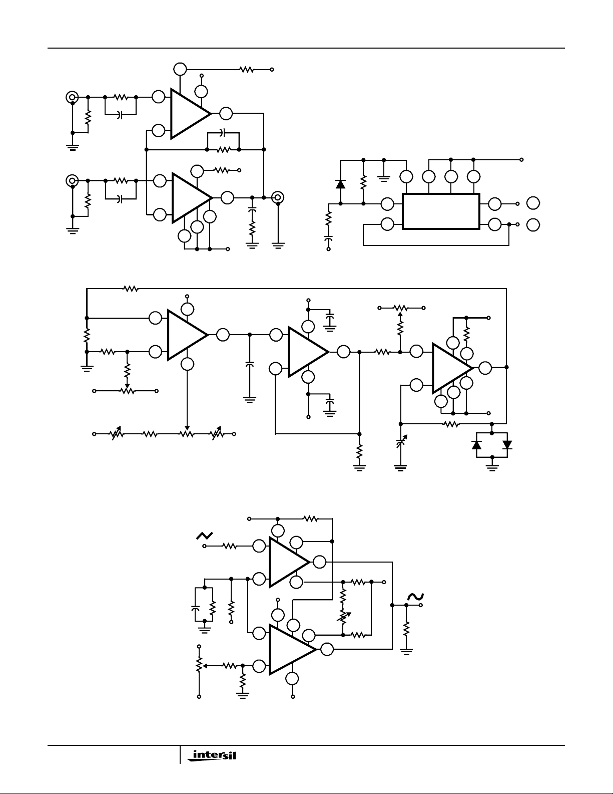
Figure 10 shows a triangle wave to sine wave converter
using the CA3280. Two 100kΩ resistors are connected
between the differential amplifier emitters and V+ to reduce
the current flow through the differential amplifier. This allows
the amplifier to fully cut off during peak input signal
excursions. THD is appropriately 0.37% for this circuit.
R
D
VOA
I
I
ABC
D
FIGURE 4. VOA SHOWING LINEARIZATION DIODES AND
FIGURE 5. BLOCK DIAGRAM OF LINEARIZED VOA
CURRENT DRIVE
10V
DIFFERENTIAL
INPUT
2kΩ
2kΩ
600Ω
V+
V-
P-P
INPUT
10kΩ
330kΩ
10kΩ
68kΩ
16
15
20kΩ
VOLTAGE
CONTROL
1
+
1/2
CA3280
-
3
+15V
68kΩ
14
3
16
+
1/2
CA3280
-
15
1
13
4
-15V
10kΩ
SINGLEENDED
OUTPUT
100kΩ
14
4
V- = -15V
V+ = +15V
OUTPUT
21V
P-P
14mV AGC
FEEDTHRU
400µV
NOISE AT
MAX GAIN
13
15kΩ
FIGURE 6. DIFFERENTIAL TO SINGLE ENDED CONVERTER FIGURE 7. TYPICAL GAIN CONTROL CIRCUIT
6
Page 7
51Ω
2kΩ
33pF
CA3280, CA3280A
3
+15V
+
1/2
CA3280
-
14
16
15
10kΩ
13
1800pF
51Ω
200Ω
V+
MAX FREQ.
200Ω
10kΩ
SET
2kΩ
33pF
3.6kΩ
100kΩ
9
+
1/2
CA3280
-
10
16
+
1/2
CA3280
-
15
910kΩ
V-V+
5.6kΩ 500Ω
2kΩ
6
10kΩ
12
300pF
4
8
1
100Ω
-15V
OUTPUT
1N914
10kΩ
0.05µF
FIGURE 8. TWO CHANNEL LINEAR MULTIPLEXER
V+
14
15 - 115pF
3
1kΩ
MIN FREQ. SET
13
V-
3
2
7
+
CA3160
-
4
V- = -7.5V
V+ = +7.5V
0.1µF
6
0.1µF
100kΩ
3.3kΩ
2kΩ
14 4 6 7
3
5
100kΩ
1/2 CD4013
V-V+
560kΩ
10
9
4 - 60pF
2.7kΩ
11
6
-
1/2
CA3280
+
1
3.3kΩ
12
8
4
1N914 1N914
-15V
TO 10kΩ
1
2
V+
V-
3
TO 10kΩ
6
FIGURE 9. CA3280 USED IN CONJUNCTION WITH A CA3160 TO PROVIDE A FUNCTION GENERATOR WITH A TUNABLE RANGE OF
2Hz TO 1MHz
0.1
µF
100kΩ
-15V
P-P
1
MΩ
+15V
2kΩ
-15V
1MΩ
6.8
MΩ
2kΩ
16
15
10
9
14
+
1/2
CA3280
-
+15V
11
+
1/2
CA3280
-
30kΩ
3
13
2
6
7
4
-15V
100kΩ
+15V
51Ω
200Ω
100kΩ
12
3.9
kΩ
170mV
+15V
FIGURE 10. TRIANGLE WAVE-TO-SINE WAVE CONVERTER
7
Page 8
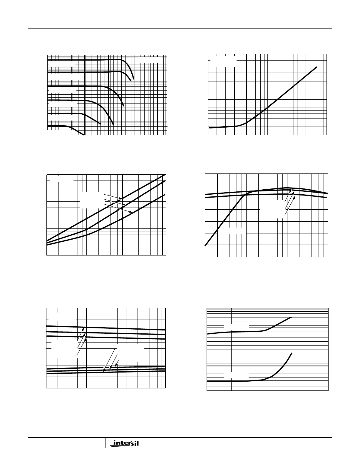
Typical Performance Curves
CA3280, CA3280A
5
10
4
10
3
10
2
10
1
10
SMALL SIGNAL FORW ARD
TRANSCONDUCTANCE (mS)
1
0.1
10
I
ABC
I
ABC
I
ABC
I
ABC
I
ABC
I
= 0.03µA
ABC
1102
= 3mA
= 300µA
= 30µA
= 3.0µA
= 0.3µA
10310410510610710810
FREQUENCY (Hz)
TA = 25oC
9
1
10
TA = 25oC
V
= ±15V
S
1
-1
10
SUPPLY CURRENT (mA)
-2
10
-1
10
1
10
DIODE CURRENT (µA)
1
FIGURE 11. AMPLIFIER GAIN vs FREQUENCY FIGURE 12. SUPPLY CURRENT vs DIODE CURRENT
3
10
VS= ±15V
TA= -55oC
= 25oC
2
10
1
10
T
T
A
A
= 125oC
2
1
0
TA = 125oC
-1
= 25oC
T
A
TA = -55oC
-2
-3
TA = 125oC
2
10
3
10
INPUT OFFSET CURRENT (nA)
1
1
1
10
2
10
AMPLIFIER BIAS CURRENT (µA)
FIGURE 13. INPUT OFFSET CURRENT vs AMPLIFIER BIAS
CURRENT
16
VS= ±15V
15
14
13
-13
0
TA = 125oC
T
= 25oC
A
T
= -55oC
A
TA = 125oC
T
= 25oC
A
T
= -55oC
A
-14
-15
PEAK OUTPUT VOLTAGE (V)
-16
1
1
10
2
10
AMPLIFIER BIAS CURRENT (µA)
FIGURE 15. PEAK OUTPUT VOLTAGE vs AMPLIFIER BIAS
CURRENT
-4
INPUT OFFSET VOLTAGE (mV)
3
10
-5
1
1
10
2
10
3
10
AMPLIFIER BIAS CURRENT (µA)
FIGURE 14. INPUT OFFSET VOLTAGE vs AMPLIFIER BIAS
CURRENT
6
10
5
10
4
10
3
10
2
10
TA = 125oC
INPUT CURRENT (pA)
1
10
3
10
1
012345678910
TA = 25oC
DIFFERENTIAL INPUT VOLTAGE (V)
FIGURE 16. INPUT CURRENT vs INPUT DIFFERENTIAL
VOLTAGE
8
Page 9
CA3280, CA3280A
Typical Performance Curves (Continued)
4
10
3
10
2
10
V9 = V10 = V12 = 30V
10
1
LEAKAGE CURRENT (nA)
-1
10
-2
10
V9 = V10 = V12 = 0V
-75 -50 -25 0 25 50 75 100 125 150 175
TEMPERATURE (oC)
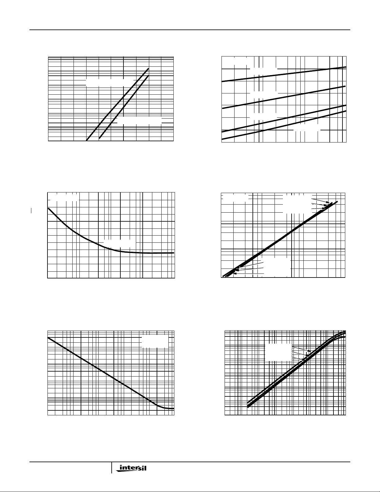
FIGURE 17. LEAKAGE CURRENT vs TEMPERATURE FIGURE 18. AMPLIFIER BIAS VOLTAGE vs AMPLIFIER BIAS
1800
1600
1400
1200
1000
800
600
AMPLIFIER BIAS VOLTAGE (mV)
400
VS= ±15V
1
CURRENT
TA = -55oC
TA = 25oC
TA = 100oC
TA = 125oC
1
10
2
10
AMPLIFIER BIAS CURRENT (µA)
3
10
1/ f NOISE VOLTAGE (nV/√Hz)
DIODE RESISTANCE (Ω)
24
22
20
18
16
14
12
10
10
10
10
10
10
3
10
10
10
2
1
VS= ±15V
TA = -55oC
= 25oC
T
A
T
= 125oC
A
8
TA = 25oC
I
ABC
= 500µA
6
4
2
0
1
10
2
10
3
10
4
10
5
10
PEAK OUTPUT CURRENT (µA)
1
1
FREQUENCY (Hz)
TA = 125oC
T
= -55oC
A
= 25oC
T
A
1
10
10
AMPLIFIER BIAS CURRENT (µA)
FIGURE 19. 1/f NOISE vs FREQUENCY FIGURE 20. PEAK OUTPUT CURRENT vs AMPLIFIER BIAS
CURRENT
SMALL SIGNAL FORW ARD
TRANSCONDUCTANCE (µmS)
5
10
4
10
3
10
2
10
1
10
TA = -55oC
T
= 25oC
A
T
= 125oC
A
1
6
TA = +25oC
= +15V
V
5
4
3
2
S
2
3
10
1
10
-1
10
1
1
10
2
10
3
10
4
10
DIODE CURRENT (µA)
-1
10
-3
10
10-210
-1
1
1
10
2
10
10310
AMPLIFIER BIAS CURRENT (µA)
FIGURE 21. DIODE RESISTANCE vs DIODE CURRENT FIGURE 22. AMPLIFIER GAIN vs AMPLIFIER BIAS CURRENT
9
4
Page 10
Typical Performance Curves (Continued)
CA3280, CA3280A
4
10
VS= ±15V
3
10
2
10
-1
TA = 125oC
TA = -55oC, 25oC
1
AMPLIFIER BIAS CURRENT (µA)
1
10
2
10
3
10
1
10
SUPPLY CURRENT (µA)
1
-1
10
10
4
10
VS= ±15V
3
10
2
10
10
INPUT BIAS CURRENT (nA)
1
TA = 125oC
1
TA = -55oC
-1
10
1
AMPLIFIER BIAS CURRENT (µA)
TA = 25oC
1
10
2
10
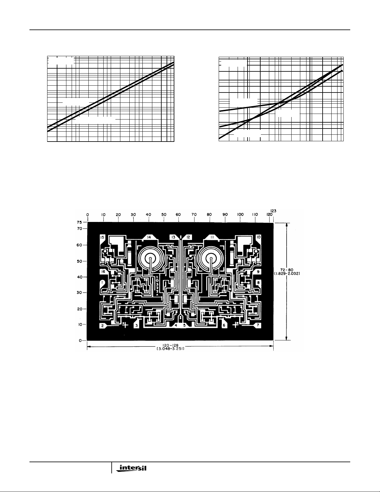
FIGURE 23. SUPPLY CURRENT vs AMPLIFIER BIAS CURRENT FIGURE 24. INPUT BIAS CURRENT vs AMPLIFIER BIAS
CURRENT
Metallization Mask Layout
3
10
10
Dimensions in parentheses are in millimeters and derived from
the basic inch dimensions as indicated. Grid graduations are in
mils (10-3 inch).
The photographs and dimensions represent a chip when it is
part of the wafer. When the wafer is cut into chips, the cleavage
angles are 57oinstead of 90owith respect to the face of the
chip. Therefore, the isolated chip is actually 7 mils (0.17mm)
larger in both dimensions.
 Loading...