

Page 1
SEMICONDUCTOR
November 1996
CA3140, CA3140A
4.5MHz, BiMOS Operational Amplifier
with MOSFET Input/Bipolar Output
Features
• MOSFET Input Stage
- Very High Input Impedance (Z
- Very Low Input Current (I
- Wide Common Mode Input Voltage Range (V
) -1.5TΩ (Typ)
IN
) -10pA (Typ) at ±15V
l
lCR
) - Can
be Swung 0.5V Below Negative Supply Voltage Rail
- Output Swing Complements Input Common Mode
Range
• Directly Replaces Industry Type 741 in Most
Applications
Applications
• Ground-Referenced Single Supply Amplifiers in Automobile and Portable Instrumentation
• Sample and Hold Amplifiers
• Long Duration Timers/Multivibrators
(µseconds-Minutes-Hours)
• Photocurrent Instrumentation
• Peak Detectors
• Active Filters
• Comparators
• Interface in 5V TTL Systems and Other Low
Supply Voltage Systems
• All Standard Operational Amplifier Applications
• Function Generators
• Tone Controls
• Power Supplies
• Portable Instruments
• Intrusion Alarm Systems
Description
The CA3140A and CA3140 are integrated circuit operational amplifiers that combine the advantages of high voltage PMOS transistors with high voltage bipolar transistors on a single monolithic chip.
The CA3140A and CA3140 BiMOS operational amplifiers feature
gate protected MOSFET (PMOS) transistors in the input circuit to
provide very high input impedance, very low input current, and
high speed performance. The CA3140A and CA3140 operate at
supply voltage from 4V to 36V (either single or dual supply).
These operational amplifiers are internally phase compensated to
achieve stable operation in unity gain follower operation, and
additionally, have access terminal for a supplementary external
capacitor if additional frequency roll-off is desired. Terminals are
also provided for use in applications requiring input offset voltage
nulling. The use of PMOS field effect transistors in the input stage
results in common mode input voltage capability down to 0.5V
below the negative supply terminal, an important attribute for single supply applications. The output stage uses bipolar transistors
and includes built-in protection against damage from load terminal short circuiting to either supply rail or to ground.
The CA3140 Series has the same 8-lead pinout used for the “741”
and other industry standard op amps. The CA3140A and CA3140
are intended for operation at supply voltages up to 36V (±18V).
Ordering Information
PART NUMBER
(BRAND)
CA3140AE -55 to 125 8 Ld PDIP E8.3
CA3140AM
(3140A)
CA3140AS -55 to 125 8 Pin Metal Can T8.C
CA3140AT -55 to 125 8 Pin Metal Can T8.C
CA3140E -55 to 125 8 Ld PDIP E8.3
CA3140M
(3140)
CA3140M96
(3140)
CA3140T -55 to 125 8 Pin Metal Can T8.C
TEMP.
RANGE (oC) PACKAGE
-55 to 125 8 Ld SOIC M8.15
-55 to 125 8 Ld SOIC M8.15
-55 to 125 8 Ld SOIC Tape
and Reel
PKG.
NO.
Pinouts
CA3140 (METAL CAN)
TOP VIEW
TAB
OFFSET
INPUT
NON-INV.
CAUTION: These devices are sensitive to electrostatic discharge. Users should follow proper IC Handling Procedures.
Copyright
© Harris Corporation 1996
NULL
INV.
INPUT
1
-
2
+
3
STROBE
8
V+
7
6
OFFSET
5
4
V- AND CASE
NULL
OUTPUT
OFFSET
INV. INPUT
NON-INV.
3-79
CA3140 (PDIP, SOIC)
1
NULL
2
3
INPUT
4
V-
TOP VIEW
-
+
8
STROBE
7
V+
6
OUTPUT
OFFSET
5
NULL
File Number 957.3
Page 2

CA3140, CA3140A
Absolute Maximum Ratings Thermal Information
DC Supply Voltage (Between V+ and V- Terminals). . . . . . . . . . 36V
Differential Mode Input Voltage. . . . . . . . . . . . . . . . . . . . . . . . . . . 8V
DC Input Voltage . . . . . . . . . . . . . . . . . . . . . . (V+ +8V) To (V- -0.5V)
Input Terminal Current . . . . . . . . . . . . . . . . . . . . . . . . . . . . . . . .1mA
Output Short Circuit Duration (Note 2). . . . . . . . . . . . . . . . Indefinite
Operating Conditions
Temperature Range . . . . . . . . . . . . . . . . . . . . . . . . -55oC to 125oC
CAUTION: Stresses above those listed in “Absolute Maximum Ratings” may cause permanent damage to the device. This is a stress only rating and operation
of the device at these or any other conditions above those indicated in the operational sections of this specification is not implied.
NOTES:
1. θJA is measured with the component mounted on an evaluation PC board in free air.
2. Short circuit may be applied to ground or to either supply.
Thermal Resistance (Typical, Note 1) θJA (oC/W) θJC (oC/W)
PDIP Package. . . . . . . . . . . . . . . . . . . 100 N/A
SOIC Package. . . . . . . . . . . . . . . . . . . 160 N/A
Metal Can Package. . . . . . . . . . . . . . . 170 85
Maximum Junction Temperature (Metal Can Package) . . . . . . . 175oC
Maximum Junction Temperature (Plastic Package) . . . . . . . .150oC
Maximum Storage Temperature Range . . . . . . . . . -65oC to 150oC
Maximum Lead Temperature (Soldering 10s) . . . . . . . . . . . . .300oC
(SOIC - Lead Tips Only)
Electrical Specifications V
= ±15V, TA = 25oC
SUPPLY
TYPICAL VALUES
PARAMETER SYMBOL TEST CONDITIONS
Input Offset Voltage Adjustment Resistor Typical Value of Resistor
4.7 18 kΩ
UNITSCA3140 CA3140A
Between Terminals 4 and 5 or
Input Resistance R
Input Capacitance C
Output Resistance R
Equivalent Wideband Input Noise Voltage, (See Figure 27) e
Equivalent Input Noise Voltage (See Figure 35) e
4 and 1 to Adjust Max V
I
I
O
BW = 140kHz, RS = 1MΩ 48 48 µV
N
RS = 100Ω f = 1kHz 40 40 nV/√Hz
N
IO
1.5 1.5 TΩ
44pF
60 60 Ω
f = 10kHz 12 12 nV/√Hz
Short Circuit Current to Opposite Supply IOM+ Source 40 40 mA
IOM- Sink 18 18 mA
Gain-Bandwidth Product, (See Figures 6, 30) f
T
4.5 4.5 MHz
Slew Rate, (See Figure 31) SR 9 9 V/µs
Sink Current From Terminal 8 To Terminal 4 to Swing Output Low 220 220 µA
Transient Response (See Figure 28) t
Settling Time at 10V
, (See Figure 5) t
P-P
RL = 2kΩ
r
CL = 100pF
OS Overshoot 10 10 %
RL = 2kΩ
S
CL = 100pF
Voltage Follower
Rise Time 0.08 0.08 µs
To 1mV 4.5 4.5 µs
To 10mV
1.4 1.4 µs
Electrical Specifications For Equipment Design, at V
= ±15V, TA = 25oC, Unless Otherwise Specified
SUPPLY
CA3140 CA3140A
PARAMETER SYMBOL
UNITSMIN TYP MAX MIN TYP MAX
Input Offset Voltage |VIO|- 5 15- 2 5mV
Input Offset Current |IIO| - 0.5 30 - 0.5 20 pA
Input Current I
Large Signal Voltage Gain (Note 3)
(See Figures 6, 29)
Common Mode Rejection Ratio
CMRR - 32 320 - 32 320 µV/V
(See Figure 34)
Common Mode Input Voltage Range (See Figure 8) V
A
I
OL
ICR
- 10 50 - 10 40 pA
20 100 - 20 100 - kV/V
86 100 - 86 100 - dB
70 90 - 70 90 - dB
-15 -15.5 to +12.5 11 -15 -15.5 to +12.5 12 V
3-80
Page 3
CA3140, CA3140A
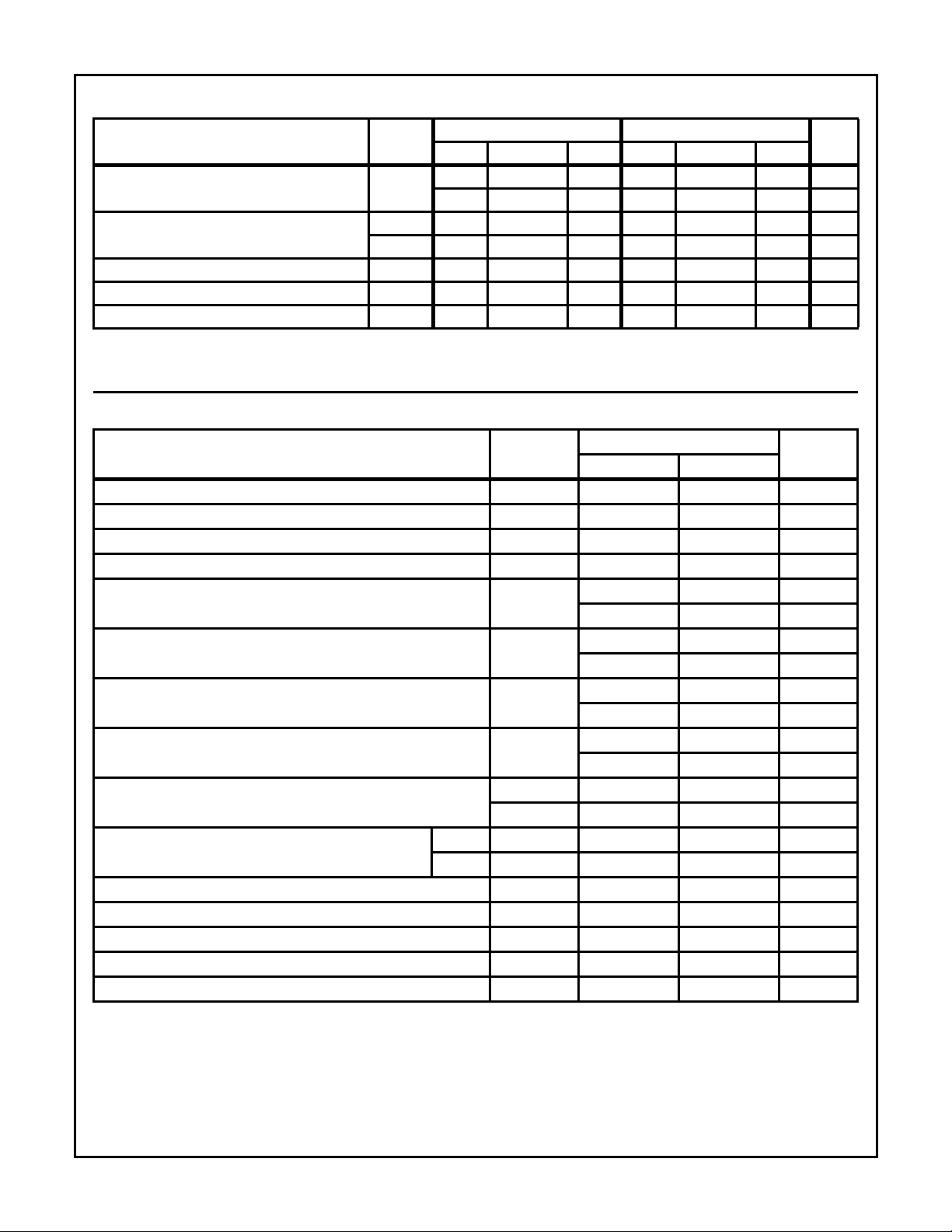
Electrical Specifications For Equipment Design, at V
= ±15V, TA = 25oC, Unless Otherwise Specified (Continued)
SUPPLY
CA3140 CA3140A
PARAMETER SYMBOL
Power-Supply Rejection Ratio,
∆VIO/∆VS (See Figure 36)
Max Output Voltage (Note 4)
(See Figures 2, 8)
PSRR - 100 150 - 100 150 µV/V
76 80 - 76 80 - dB
VOM+ +12 13 - +12 13 - V
VOM- -14 -14.4 - -14 -14.4 - V
UNITSMIN TYP MAX MIN TYP MAX
Supply Current (See Figure 32) I+ - 4 6 - 4 6 mA
Device Dissipation P
D
- 120 180 - 120 180 mW
Input Offset Voltage Temperature Drift ∆VIO/∆T-8--6-µV/oC
NOTES:
3. At VO = 26V
, +12V, -14V and RL = 2kΩ.
P-P
4. At RL = 2kΩ.
Electrical Specifications For Design Guidance At V+ = 5V, V- = 0V, T
= 25oC
A
TYPICAL VALUES
PARAMETER SYMBOL
Input Offset Voltage |V
|5 2mV
IO
UNITSCA3140 CA3140A
Input Offset Current |IIO| 0.1 0.1 pA
Input Current I
Input Resistance R
Large Signal Voltage Gain (See Figures 6, 29) A
I
I
OL
22pA
11TΩ
100 100 kV/V
100 100 dB
Common Mode Rejection Ratio CMRR 32 32 µV/V
90 90 dB
Common Mode Input Voltage Range (See Figure 8) V
ICR
-0.5 -0.5 V
2.6 2.6 V
Power Supply Rejection Ratio PSRR
∆VI0/∆V
S
100 100 µV/V
80 80 dB
Maximum Output Voltage (See Figures 2, 8) VOM+3 3 V
V
- 0.13 0.13 V
OM
Maximum Output Current: Source IOM+10 10mA
Sink
I
-1 1mA
OM
Slew Rate (See Figure 31) SR 7 7 V/µs
Gain-Bandwidth Product (See Figure 30) f
T
3.7 3.7 MHz
Supply Current (See Figure 32) I+ 1.6 1.6 mA
Device Dissipation P
D
88mW
Sink Current from Terminal 8 to Terminal 4 to Swing Output Low 200 200 µA
3-81
Page 4
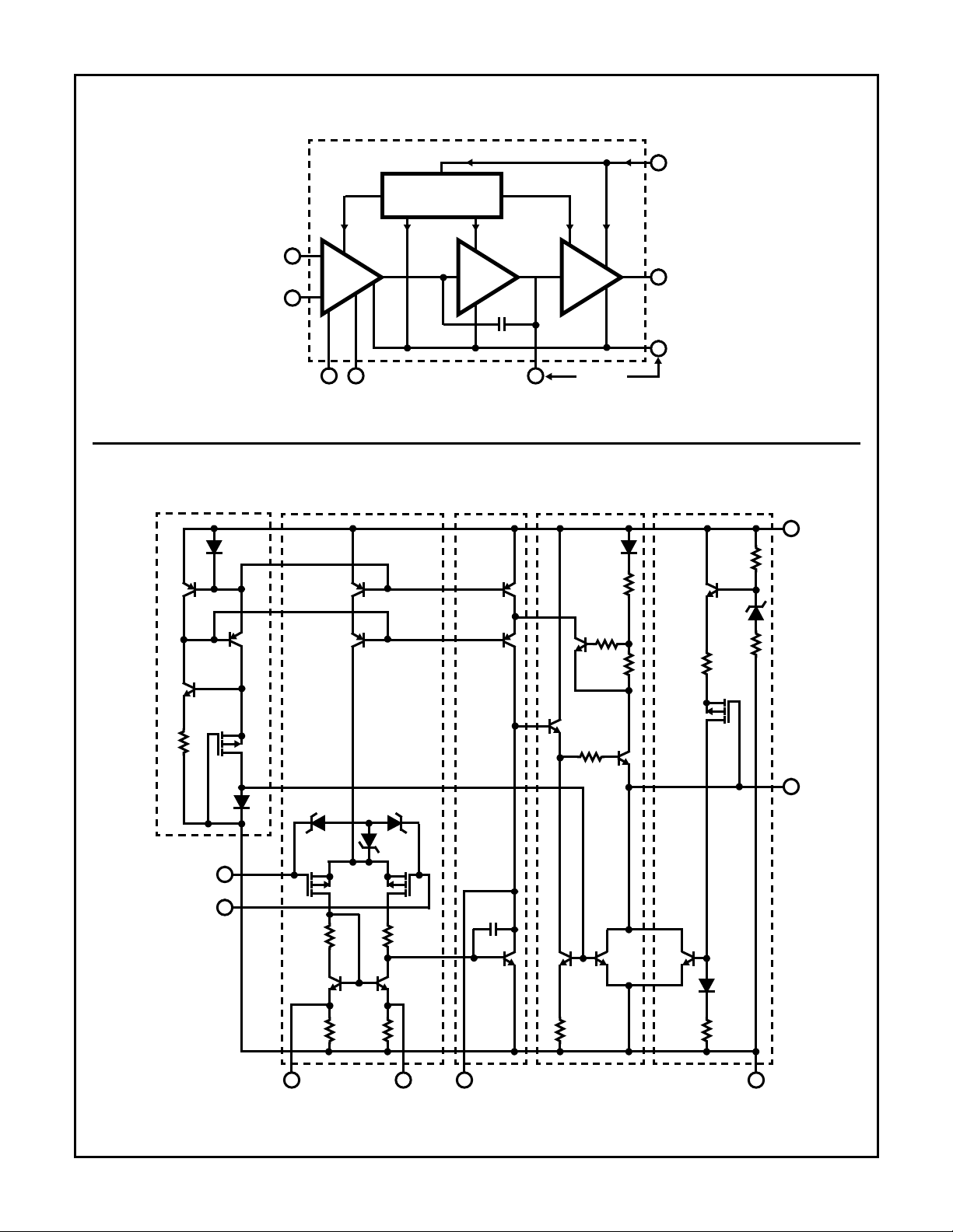
Block Diagram
CA3140, CA3140A
Schematic Diagram
D
1
Q
1
Q
6
Q
7
+
3
INPUT
-
2
2mA 4mA
BIAS CIRCUIT
CURRENT SOURCES
AND REGULATOR
200µA 200µA1.6mA 2µA 2mA
≈
A ≈10
A
10,000
C
1
12pF
5
1 8
OFFSET
NULL
Q
Q
2
Q
5
3
Q
4
A ≈1
STROBE
Q
19
50Ω
R
1K
20Ω
V+
7
OUTPUT
6
V-
4
DYNAMIC CURRENT SINKOUTPUT STAGESECOND STAGEINPUT STAGEBIAS CIRCUIT
7
V+
D
7
R
9
10
R
11
Q
R
12K
R
13
5K
20
D
8
R
14
20K
12
R
1
8K
INVERTING
INPUT
NON-INVERTING
INPUT
Q
8
D
2
2
-
+
3
R
500Ω
Q
R
500Ω
5 1 8
NOTE: All resistance values are in ohms.
Q
Q
17
R
8
1K
Q
18
D
3
2
11
4
D
4
D
5
Q
Q
10
9
C
12pF
1
Q
Q
13
14
R
50Ω
Q
15
6
R
500Ω
R
3
500Ω
Q
12
5
21
6
OUTPUT
Q
16
D
6
R
7
30Ω
4
STROBEOFFSET NULL
V-
3-82
Page 5

CA3140, CA3140A
Application Information
Circuit Description
As shown in the block diagram, the input terminals may be
operated down to 0.5V below the negative supply rail. Two
class A amplifier stages provide the voltage gain, and a
unique class AB amplifier stage provides the current gain
necessary to drive low-impedance loads.
A biasing circuit provides control of cascoded constant current
flow circuits in the first and second stages. The CA3140
includes an on chip phase compensating capacitor that is
sufficient for the unity gain voltage follower configuration.
Input Stage
The schematic diagram consists of a differential input stage
using PMOS field-effect transistors (Q
mirror pair of bipolar transistors (Q
resistors together with resistors R
transistors also function as a differential-to-single-ended
converter to provide base current drive to the second stage
bipolar transistor (Q
). Offset nulling, when desired, can be
13
effected with a 10kΩ potentiometer connected across
Terminals 1 and 5 and with its slider arm connected to Terminal
4. Cascode-connected bipolar transistors Q
constant current source for the input stage. The base biasing
circuit for the constant current source is described
subsequently. The small diodes D
protection against high voltage transients, e.g., static electricity.
Second Stage
Most of the voltage gain in the CA3140 is provided by the
second amplifier stage, consisting of bipolar transistor Q
and its cascode connected load resistance provided by
bipolar transistors Q
, Q4. On-chip phase compensation,
3
sufficient for a majority of the applications is provided by C
Additional Miller-Effect compensation (roll off) can be
accomplished, when desired, by simply connecting a small
capacitor between Terminals 1 and 8. Terminal 8 is also
used to strobe the output stage into quiescence. When
terminal 8 is tied to the negative supply rail (Terminal 4) by
mechanical or electrical means, the output Terminal 6
swings low, i.e., approximately to Terminal 4 potential.
Output Stage
The CA3140 Series circuits employ a broad band output stage
that can sink loads to the negative supply to complement the
capability of the PMOS input stage when operating near the
negative rail. Quiescent current in the emitter-follower cascade
circuit (Q
, Q18) is established by transistors (Q14, Q15)
17
whose base currents are “mirrored” to current flowing through
diode D
in the bias circuit section. When the CA3140 is
2
operating such that output Terminal 6 is sourcing current,
transistor Q
functions as an emitter-follower to source current
18
from the V+ bus (Terminal 7), via D
conditions, the collector potential of Q
permit the necessary flow of base current to emitter follower
Q
which, in turn, drives Q18.
17
When the CA3140 is operating such that output Terminal 6 is
sinking current to the V- bus, transistor Q
sinking element. Transistor Q
is mirror connected to D6, R7,
16
, Q10) working into a
9
, Q12) functioning as load
11
through R5. The mirror pair
2
, Q5 are the
2
, D4, D5 provide gate oxide
3
, R9, and R11. Under these
7
is sufficiently high to
13
is the current
16
13
1
with current fed by wa y of Q
turn, is biased by current flow through R
, R12, and Q20. Transistor Q20, in
21
, zener D8, and R14.
13
The dynamic current sink is controlled by voltage le vel sensing.
For purposes of explanation, it is assumed that output Terminal
6 is quiescently established at the potential midpoint between
the V+ and V- supply rails. When output current sinking mode
operation is required, the collector potential of transistor Q
driven below its quiescent level, thereby causing Q
17
decrease the output voltage at Terminal 6. Thus, the gate
terminal of PMOS transistor Q
thereby reducing the channel resistance of Q
is displaced toward the V- bus,
21
21
consequence, there is an incremental increase in current flow
through Q
result, Q
, R12, Q21, D6, R7, and the base of Q16. As a
20
sinks current from Terminal 6 in direct response to
16
the incremental change in output voltage caused by Q
sink current flows regardless of load; any excess current is
internally supplied by the emitter-follower Q
protection of the output circuit is provided by Q
. Short circuit
18
, which is
19
driven into conduction by the high voltage drop developed
across R
conditions, the collector of Q
reduce the base current drive from Q
flow in Q
under output short circuit conditions. Under these
11
to the short circuited load terminal.
18
diverts current from Q4 so as to
19
, thereby limiting current
17
Bias Circuit
Quiescent current in all stages (except the dynamic current
sink) of the CA3140 is dependent upon bias current flow in R
The function of the bias circuit is to establish and maintain
constant current flow through D
, Q6, Q8 and D2. D1 is a diode
1
connected transistor mirror connected in parallel with the base
emitter junctions of Q
, Q2, and Q3. D1 may be considered as a
1
current sampling diode that senses the emitter current of Q
and automatically adjusts the base current of Q6 (via Q1) to
maintain a constant current through Q
currents in Q
.
D
. Furthermore, current in diode connected transistor Q
1
, Q3 are also determined by constant current flow
2
, Q8, D2. The base
6
establishes the currents in transistors Q14 and Q15.
Typical Applications
Wide dynamic range of input and output characteristics with
the most desirable high input impedance characteristics is
achieved in the CA3140 b y the use of an unique design based
upon the PMOS Bipolar process. Input common mode voltage
range and output swing capabilities are complementary,
allowing operation with the single supply down to 4V.
The wide dynamic range of these parameters also means
that this device is suitable for many single supply applications, such as, for example, where one input is driven below
the potential of Terminal 4 and the phase sense of the output
signal must be maintained – a most important consideration
in comparator applications.
Output Circuit Considerations
Excellent interfacing with TTL circuitry is easily achieved with a
single 6.2V zener diode connected to Terminal 8 as shown in
Figure 1. This connection assures that the maximum output signal swing will not go more positiv e than the zener voltage minus
two base-to-emitter voltage drops within the CA3140. These
voltages are independent of the operating supply v oltage .
is
13
, Q18 to
. As a
. This
18
.
1
6
2
3-83
Page 6

CA3140, CA3140A
V+
5V TO 36V
2
3
7
CA3140
8
6.2V
6
4
≈5V
LOGIC
SUPPLY
5V
TYPICAL
TTL GATE
FIGURE 1. ZENER CLAMPING DIODE CONNECTED TO
TERMINALS 8 AND 4 TO LIMIT CA3140 OUTPUT
SWING TO TTL LEVELS
1000
)
16
, Q
15
SATURATION VOLTAGE (mV)
OUTPUT STAGE TRANSISTOR (Q
FIGURE 2. VOLTAGE ACROSS OUTPUT TRANSISTORS (Q
SUPPLY VOLTAGE (V-) = 0V
T
= 25oC
A
SUPPLY VOLTAGE (V+) = +5V
100
10
1
0.01 0.1
LOAD (SINKING) CURRENT (mA)
+15V
+30V
1.0 10
15
AND Q16) vs LOAD CURRENT
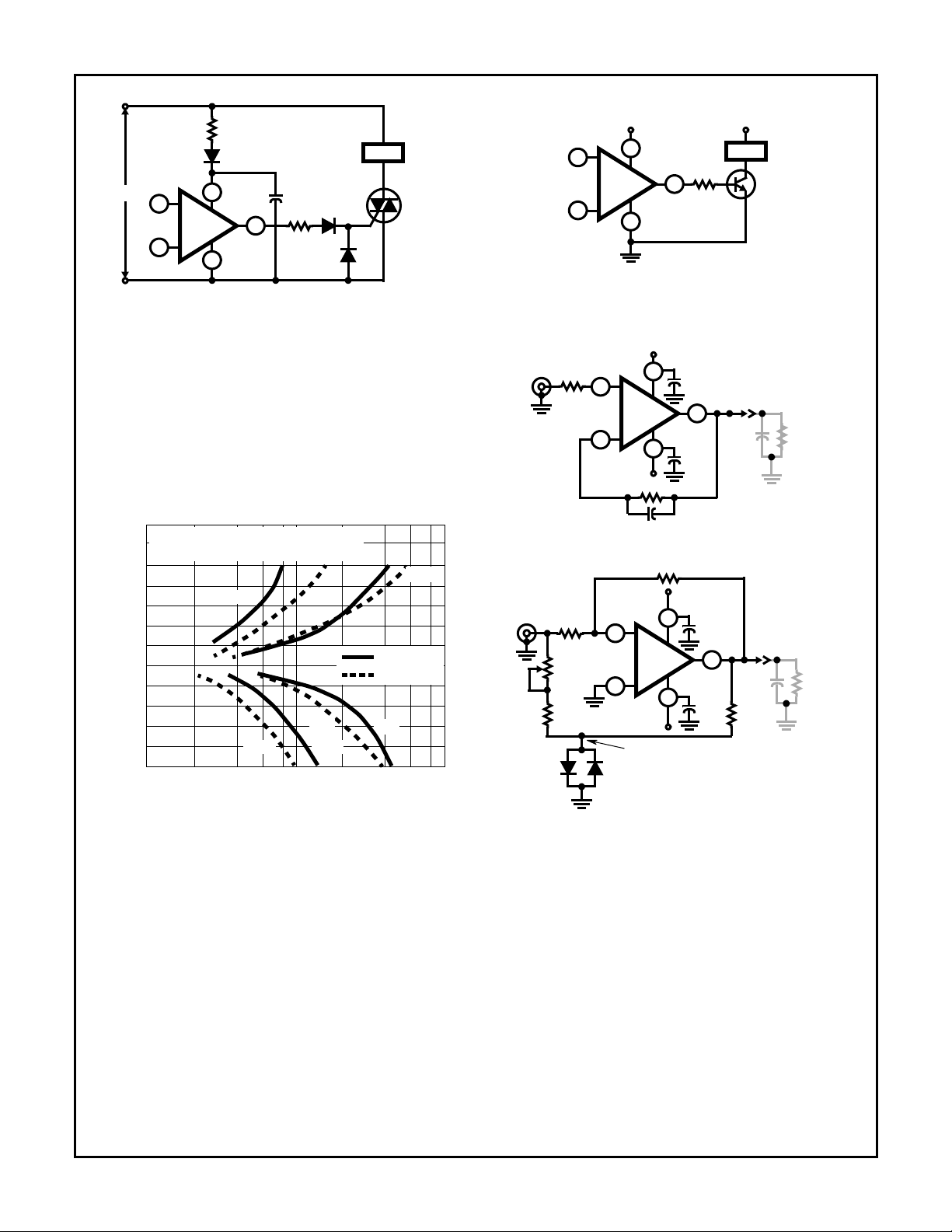
Figure 2 shows output current sinking capabilities of the
CA3140 at various supply voltages. Output voltage swing to
the negative supply rail permits this device to operate both
power transistors and thyristors directly without the need for
level shifting circuitry usually associated with the 741 series
of operational amplifiers.
Figure 4 shows some typical configurations. Note that a
series resistor, R
, is used in both cases to limit the drive
L
available to the driven device. Moreover, it is recommended
that a series diode and shunt diode be used at the thyristor
input to prevent large negative transient surges that can
appear at the gate of thyristors, from damaging the
integrated circuit.
Offset Voltage Nulling
The input offset voltage can be nulled by connecting a 10kΩ
potentiometer between Terminals 1 and 5 and retur ning its
wiper arm to terminal 4, see Figure 3A. This technique, however, gives more adjustment range than required and therefore, a considerable portion of the potentiometer rotation is
not fully utilized. Typical values of series resistors (R) that
may be placed at either end of the potentiometer, see Figure
3B, to optimize its utilization range are given in the Electrical
Specifications table.
An alternate system is shown in Figure 3C. This circuit uses
only one additional resistor of approximately the value
shown in the table. For potentiometers, in which the resistance does not drop to 0Ω at either end of rotation, a value of
resistance 10% lower than the values shown in the table
should be used.
Low Voltage Operation
Operation at total supply voltages as low as 4V is possible
with the CA3140. A current regulator based upon the PMOS
threshold voltage maintains reasonable constant operating
current and hence consistent performance down to these
lower voltages.
The low voltage limitation occurs when the upper extreme of
the input common mode voltage range extends down to the
voltage at Terminal 4. This limit is reached at a total supply
voltage just below 4V. The output voltage range also begins to
extend down to the negative supply rail, but is slightly higher
than that of the input. Figure 8 shows these characteristics and
shows that with 2V dual supplies, the lower e xtreme of the input
common mode voltage range is below ground potential.
V+
2
3
10kΩ
CA3140
5
1
7
6
4
V-
2
CA3140
3
R
10kΩ
V+
7
6
4
5
1
R
V-
2
3
10kΩ
CA3140
5
1
R
V+
7
6
4
V-
FIGURE 3A. BASIC FIGURE 3B. IMPROVED RESOLUTION FIGURE 3C. SIMPLER IMPROVED
RESOLUTION
FIGURE 3. THREE OFFSET VOLTAGE NULLING METHODS
3-84
Page 7
CA3140, CA3140A
R
S
30V
6
NO LOAD
R
L
120V
AC
2
3
7
CA3140
4
FIGURE 4. METHODS OF UTILIZING THE V
LOAD RESISTANCE (RL) = 2kΩ
LOAD CAPACITANCE (C
SUPPLY VOLTAGE: VS = ±15V
T
= 25oC
A
10
8
6
4
2
0
-2
-4
INPUT VOLTAGE (V)
-6
-8
-10
0.1
) = 100pF
L
10mV 10mV
10mV
1.0 10
SETTLING TIME (µs)
10mV
LOAD
1mV
MT
2
MT
1
CE(SAT)
1mV
FOLLOWER
INVERTING
1mV1mV
V+ +HV
2
3
7
CA3140
4
6
LOAD
R
L
SINKING CURRENT CAPABILITY OF THE CA3140 SERIES
FOLLOWER
+15V
7
4
2kΩ
INVERTING
5kΩ
+15V
7
CA3140
4
-15V
0.1µF
6
0.1µF
0.1µF
6
0.1µF
SIMULATED
LOAD
100pF
SIMULATED
LOAD
100pF
5.11kΩ
D
1N914
10kΩ
5kΩ
200Ω
4.99kΩ
1
3
CA3140
2
-15V
0.05µF
2
3
SETTLING POINT
D
2
1N914
2kΩ
2kΩ
FIGURE 5A. WAVEFORM FIGURE 5B. TEST CIRCUITS
FIGURE 5. SETTLING TIME vs INPUT VOLTAGE
Bandwidth and Slew Rate
For those cases where bandwidth reduction is desired, for
example, broadband noise reduction, an external capacitor
connected between Terminals 1 and 8 can reduce the open
loop -3dB bandwidth. The slew rate will, however, also be
proportionally reduced by using this additional capacitor.
Thus, a 20% reduction in bandwidth by this technique will
also reduce the slew rate by about 20%.
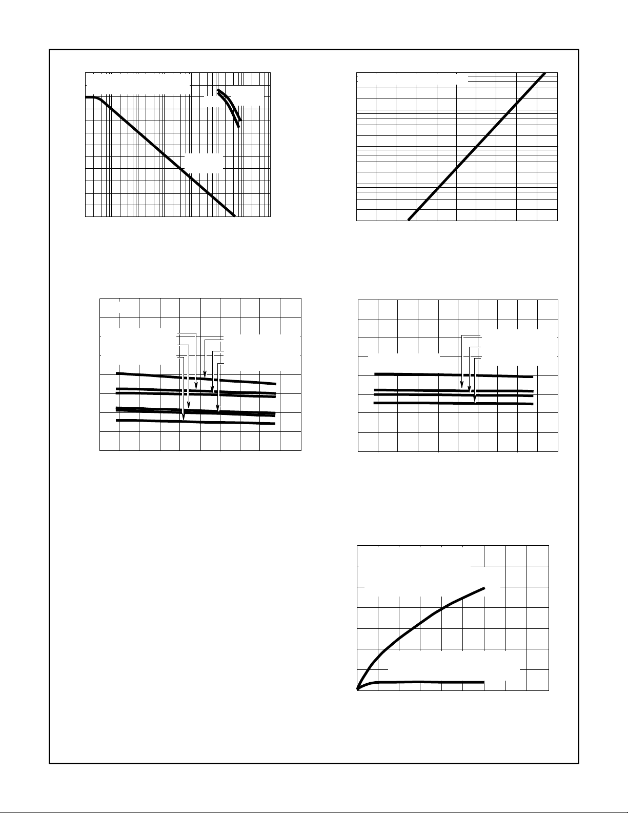
Figure 5 shows the typical settling time required to reach
1mV or 10mV of the final value for various levels of large
signal inputs for the voltage follower and inverting unity gain
amplifiers. The exceptionally fast settling time characteristics
are largely due to the high combination of high gain and wide
bandwidth of the CA3140; as shown in Figure 6.
Input Circuit Considerations
As mentioned previously, the amplifier inputs can be driven
below the Terminal 4 potential, but a series current limiting
resistor is recommended to limit the maximum input terminal
current to less than 1mA to prevent damage to the input protection circuitry.
Moreover, some current limiting resistance should be
provided between the inverting input and the output when
the CA3140 is used as a unity gain voltage follower. This
resistance prevents the possibility of extremely large input
signal transients from forcing a signal through the input
protection network and directly driving the internal constant
current source which could result in positive feedback via the
output terminal. A 3.9kΩ resistor is sufficient.
3-85
Page 8
CA3140, CA3140A
SUPPL Y VOLT AGE: VS = ±15V
T
= 25oC
A
100
80
60
40
20
OPEN LOOP VOLTAGE GAIN (dB)
0
1
10
RL = 2kΩ,
= 100pF
C
L
2
10310410510610710
10
FREQUENCY (Hz)
φOL
RL = 2kΩ,
= 0pF
C
L
FIGURE 6. OPEN LOOP VOLTAGE GAIN AND PHASE vs
FREQUENCY
RL = ∞
0
+V
AT TA = 125oC
ICR
-0.5
-1.0
-1.5
+V
+V
ICR
ICR
AT TA = 25oC
AT TA = -55oC
+V
+V
+V
OUT
OUT
OUT
AT TA = 125oC
AT TA = 25oC
AT TA = -55oC
-75
-90
-105
-120
-135
-150
8
(DEGREES)
OPEN LOOP PHASE
10K
SUPPLY VOLTAGE: VS = ±15V
1K
100
INPUT CURRENT (pA)
10
1
-60 -40 -20 0 20 40 60 80 100 120 140
TEMPERATURE (
o
C)
FIGURE 7. INPUT CURRENT vs TEMPERATURE
1.5
-V
AT TA = 125oC
1.0
0.5
-V
T
0
FOR
OUT
= -55oC to 125oC
A
ICR
-V
AT TA = 25oC
ICR
-V
AT TA = -55oC
ICR
-2.0
-2.5
FROM TERMINAL 7 (V+)
-3.0
INPUT AND OUTPUT VOLTAGE EXCURSIONS
0 5 10 15 20 25
SUPPLY VOLTAGE (V+, V-)
-0.5
FROM TERMINAL 4 (V-)
-1.0
-1.5
INPUT AND OUTPUT VOLTAGE EXCURSIONS
0 5 10 15 20 25
SUPPLY VOLTAGE (V+, V-)
FIGURE 8. OUTPUT VOLTAGE SWING CAPABILITY AND COMMON MODE INPUT VOLTAGE RANGE vs SUPPLY VOLTAGE
The typical input current is on the order of 10pA when the
inputs are centered at nominal device dissipation. As the
same magnitude as those encountered in an operational
amplifier employing a bipolar transistor input stage.
output supplies load current, device dissipation will increase,
raising the chip temperature and resulting in increased input
current. Figure 7 shows typical input terminal current versus
ambient temperature for the CA3140.
It is well known that MOSFET devices can exhibit slight
changes in characteristics (for example, small changes in
input offset voltage) due to the application of large differential input voltages that are sustained over long periods at elevated temperatures.
Both applied voltage and temperature accelerate these
changes. The process is reversible and offset voltage shifts of
the opposite polarity reverse the offset. Figure 9 shows the
typical offset voltage change as a function of various stress
voltages at the maximum rating of 125
lower temperatures (metal can and plastic), for example, at
o
85
C, this change in voltage is considerab ly less . In typical lin-
o
C (for metal can); at
ear applications, where the differential voltage is small and
7
TA = 125oC
FOR METAL CAN PACKAGES
6
DIFFERENTIAL DC VOLTAGE
(ACROSS TERMINALS 2 AND 3) = 2V
5
OUTPUT STAGE TOGGLED
4
3
2
OFFSET VOLTAGE SHIFT (mV)
1
0
0 500 1000 1500 2000 2500 3000 3500 4000 4500
DIFFERENTIAL DC VOLTAGE
(ACROSS TERMINALS 2 AND 3) = 0V
OUTPUT VOLTAGE = V+ / 2
TIME (HOURS)
FIGURE 9. TYPICAL INCREMENTAL OFFSET VOLTAGE
SHIFT vs OPERATING LIFE
symmetrical, these incremental changes are of about the
3-86
Page 9

CA3140, CA3140A
Super Sweep Function Generator
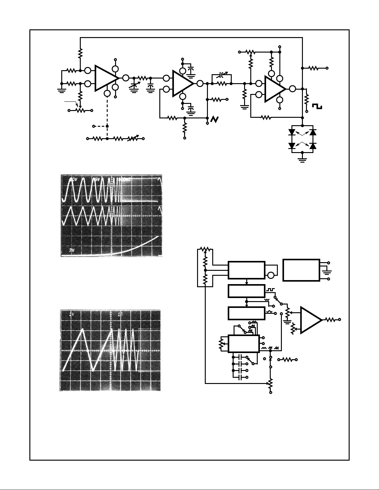
A function generator having a wide tuning range is shown in
Figure 10. The 1,000,000/1 adjustment range is accomplished by a single variable potentiometer or by an auxiliary
sweeping signal. The CA3140 functions as a non-inverting
readout amplifier of the triangular signal developed across
the integrating capacitor network connected to the output of
the CA3080A current source.
Buffered triangular output signals are then applied to a second CA3080 functioning as a high speed hysteresis switch.
Output from the switch is returned directly back to the input
of the CA3080A current source, thereby, completing the positive feedback loop
The triangular output level is determined by the four 1N914
level limiting diodes of the second CA3080 and the resistor
divider network connected to Ter minal No. 2 (input) of the
CA3080. These diodes establish the input trip level to this
switching stage and, therefore, indirectly determine the
amplitude of the output triangle.
Compensation for propagation delays around the entire loop
is provided by one adjustment on the input of the CA3080.
This adjustment, which provides for a constant generator
amplitude output, is most easily made while the generator is
sweeping. High frequency ramp linearity is adjusted by the
single 7pF to 60pF capacitor in the output of the CA3080A.
It must be emphasized that only the CA3080A is
characterized for maximum output linearity in the current
generator function.
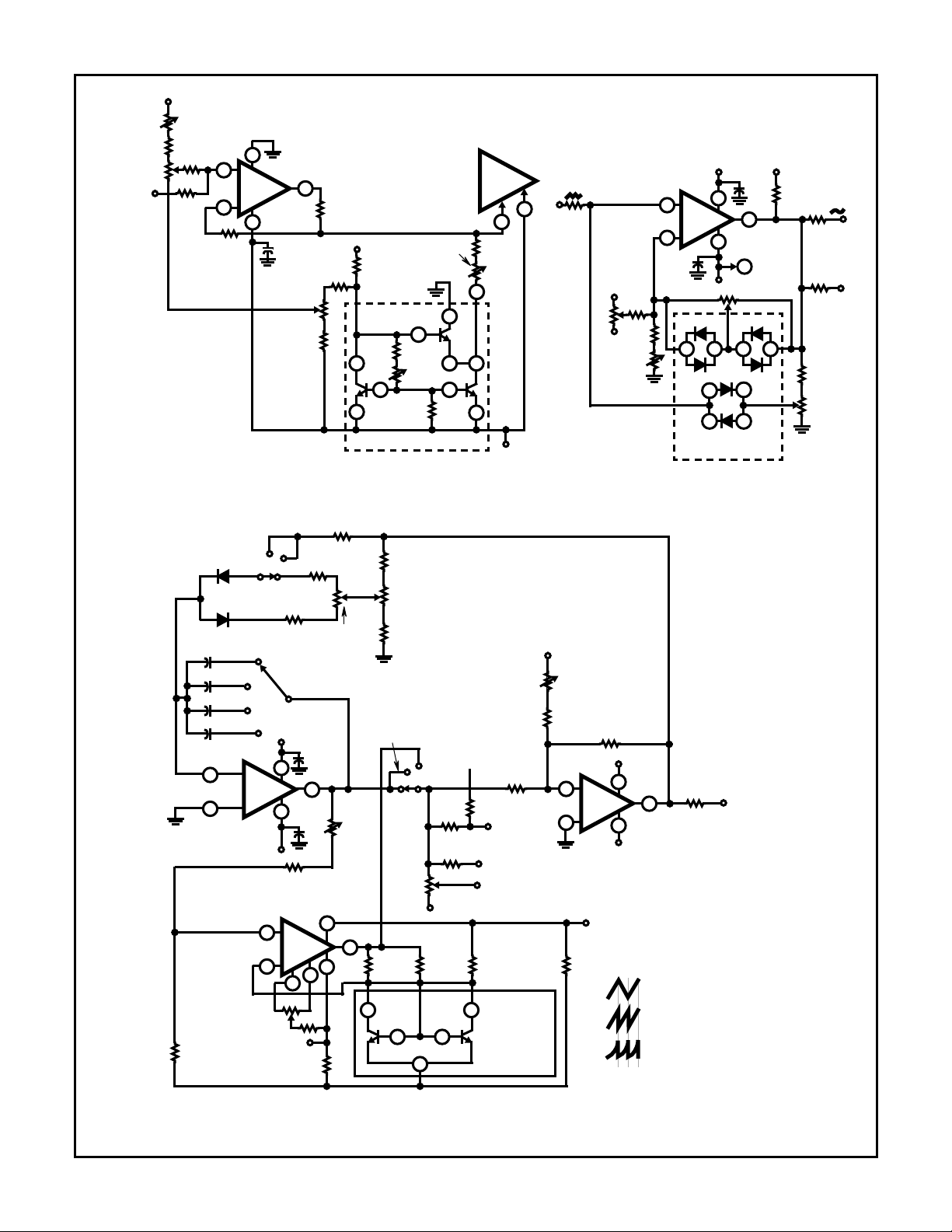
Meter Driver and Buffer Amplifier
Figure 11 shows the CA3140 connected as a meter driver
and buffer amplifier. Low driving impedance is required of
the CA3080A current source to assure smooth operation of
the Frequency Adjustment Control. This low-driving
impedance requirement is easily met by using a CA3140
connected as a voltage follower. Moreover, a meter may be
placed across the input to the CA3080A to give a logarithmic
analog indication of the function generator’s frequency.
temperature coefficients at both ends of the Frequency
Adjustment Control.
To calibrate this circuit, set the Frequency Adjustment
Potentiometer at its low end. Then adjust the Minimum
Frequency Calibration Control for the lowest frequency. To
establish the upper frequency limit, set the Frequency
Adjustment Potentiometer to its upper end and then adjust
the Maximum Frequency Calibration Control for the
maximum frequency. Because there is interaction among
these controls, repetition of the adjustment procedure may
be necessary. Two adjustments are used for the meter. The
meter sensitivity control sets the meter scale width of each
decade, while the meter position control adjusts the pointer
on the scale with negligible effect on the sensitivity
adjustment. Thus, the meter sensitivity adjustment control
calibrates the meter so that it deflects
1
/6 of full scale for
each decade change in frequency.
Sine Wave Shaper
The circuit shown in Figure 12 uses a CA3140 as a voltage
follower in combination with diodes from the CA3019 Array
to convert the triangular signal from the function generator to
a sine-wave output signal ha ving typically less than 2% THD.
The basic zero crossing slope is established by the 10kΩ
potentiometer connected between Terminals 2 and 6 of the
CA3140 and the 9.1kΩ resistor and 10kΩ potentiometer
from Ter minal 2 to ground. Two break points are established
by diodes D
through D4. Positive feedback via D5 and D
1
establishes the zero slope at the maximum and minimum
levels of the sine wa v e. This technique is necessary because
the voltage follower configuration approaches unity gain
rather than the zero gain required to shape the sine wave at
the two extremes.
6
Analog frequency readout is readily accomplished by the
means described above because the output current of the
CA3080A varies approximately one decade for each 60mV
change in the applied voltage, V
(voltage between
ABC
Terminals 5 and 4 of the CA3080A of the function generator).
Therefore, six decades represent 360mV change in V
ABC
.
Now, only the reference voltage must be established to set
the lower limit on the meter. The three remaining transistors
from the CA3086 Array used in the sweep generator are
used for this reference voltage. In addition, this reference
generator arrangement tends to track ambient temperature
variations, and thus compensates for the effects of the normal negative temperature coefficient of the CA3080A V
ABC
terminal voltage.
Another output voltage from the reference generator is used
to insure temperature tracking of the lower end of the
Frequency Adjustment Potentiometer. A large series
resistance simulates a current source, assuring similar
3-87
Page 10
CA3140, CA3140A
360Ω
360Ω
SYMMETRY
FROM BUFFER METER
DRIVER (OPTIONAL)
2MΩ
-15V
100kΩ
THIS NETWORK IS USED WHEN THE
OPTIONAL BUFFER CIRCUIT IS NOT USED
7.5kΩ
+
CA3080A
-
5
7
4
-15V
15kΩ
6
7-60
pF
HIGH
FREQ.
SHAPE
10kΩ120Ω
3
2
+15V
39kΩ
-15V +15V
+15V+15V
7
+
3
51
CA3140
pF
2
-
4
-15V
2kΩ
FREQUENCY
ADJUSTMENT
OUTPUT
AMPLIFIER
FIGURE 10A. CIRCUIT
0.1
µF
5.1kΩ
6
0.1
µF
TO
SINE WAVE
SHAPER
HIGH
FREQUENCY
LEVEL
7-60pF
11kΩ
10kΩ
EXTERNAL
OUTPUT
-15V
910kΩ
11kΩ
CENTERING
10kΩ
62kΩ
2
3
13kΩ
5
-
CA3080
+
7
4
+15V
-15V
10kΩ
EXTERNAL
OUTPUT
6
2.7kΩ
TO OUTPUT
AMPLIFIER
1N914
Top Trace: Output at junction of 2.7Ω and 51Ω resistors;
5V/Div., 500ms/Div.
Center Trace: External output of triangular function generator;
2V/Div., 500ms/Div.
Bottom Trace: Output of “Log” generator; 10V/Div., 500ms/Div.
FIGURE 10B. FIGURE FUNCTION GENERATOR SWEEPING
1V/Div., 1s/Div.
Three tone test signals, highest frequency ≥0.5MHz. Note the slight
asymmetry at the three second/cycle signal. This asymmetry is due to
slightly different positive and negative integration from the CA3080A
and from the PC board and component leakages at the 100pA level.
FIGURE 10C. FUNCTION GENERATOR WITH FIXED
FREQUENCIES
FIGURE 10. FUNCTION GENERATOR
FREQUENCY
ADJUSTMENT
FINE
RATE
COARSE
METER DRIVER
AND BUFFER
AMPLIFIER
GENERATOR
SINE WAVE
GENERATOR
RATE
FUNCTION
SHAPER
SWEEP
GATE
SWEEP
OFF
V-
M
INT.
SWEEP
LENGTH
V-
DC LEVEL
EXT.
ADJUST
POWER
SUPPLY ±15V
FIGURE 10D. INTERCONNECTIONS
WIDEBAND
LINE DRIVER
EXTERNAL
INPUT
+15V
-15V
51Ω
3-88
Page 11
CA3140, CA3140A
500kΩ
FREQUENCY
ADJUSTMENT
10kΩ
SWEEP IN
FREQUENCY
CALIBRATION
MAXIMUM
620kΩ
51kΩ
3MΩ
3
2
2kΩ
7
+
CA3140
-
4
0.1µF
FREQUENCY
CALIBRATION
MINIMUM
6
510Ω
4.7kΩ
12kΩ
2.4kΩ
2.5
kΩ
+15V
8
6
POSITION
7
ADJUSTMENT
TO CA3080A
OF FUNCTION
GENERATOR
(FIGURE 10)
METER
SENSITIVITY
ADJUSTMENT
11
9
510Ω
10
2kΩ
METER
3
/5 OF CA3086
12
3.6kΩ
CA3080A
620Ω
200µA
M
METER
14
13
1kΩ
5
-15V
0.1µF
6
SUBSTRATE
OF CA3019
7
-15V
D
D
D
6
1
43
D
5
-15V
5.6kΩ
4
2856
2
+15V
7
+
1MΩ
9.1kΩ
R
10kΩ
1
3
CA3140
-
2
0.1µF
D
1
D
3
CA3019
DIODE ARRA Y
4
R3 10kΩ
9
4
5.1kΩ
+15V
100
kΩ
-15V
FIGURE 11. METER DRIVER AND BUFFER AMPLIFIER FIGURE 12. SINE WAVE SHAPER
750kΩ
0.47µF
470pF
100Ω
1N914
1N914
0.047µF
4700pF
2
3
LOG
“LOG”
SAWT OOTH
-
CA3140
+
-15V
3
2
VIO
22MΩ
+15V
7
4
43kΩ
+
CA3140
-
1
25kΩ
-15V
390Ω
18MΩ
1MΩ
SAWT OO TH
SYMMETRY
COARSE
RATE
0.1
µF
6
0.1
µF
7
4
5
3.9Ω
50kΩ
LOG
RATE
ADJUST
100kΩ
FINE
100kΩ
RATE
8.2kΩ
SAWT OOTH
“LOG”
TRIANGLE
10kΩ
SWEEP WIDTH
-15V
6
51kΩ 6.8kΩ 91kΩ
3
SAWT OOTH AND
+15V
RAMP LOW LEVEL
SET (-14.5V)
50kΩ
75kΩ
+15V
100kΩ
30kΩ
10kΩ
EXTERNAL OUTPUT
36kΩ
TO OUTPUT
AMPLIFIER
3
2
-
CA3140
+
TO FUNCTION GENERATOR “SWEEP IN”
10kΩ
15
TRANSISTORS
FROM CA3086
24
ARRAY
51kΩ
+15V
+15V
7
4
-15V
10kΩ GATE
6
TRIANGLE
SAWT OOTH
“LOG”
PULSE
OUTPUT
7.5kΩ
TO
WIDEBAND
OUTPUT
AMPLIFIER
10kΩ
EXTERNAL
OUTPUT
430Ω
R
2
1kΩ
FIGURE 13. SWEEPING GENERATOR
3-89
Page 12
CA3140, CA3140A
This circuit can be adjusted most easily with a distortion
analyzer, but a good first approximation can be made by
comparing the output signal with that of a sine wave
generator. The initial slope is adjusted with the
potentiometer R
slope is established by adjusting R
additional segments that are contributed by these diodes.
Because there is some interaction among these controls,
repetition of the adjustment procedure may be necessary.
Sweeping Generator
, followed by an adjustment of R2. The final
1
, thereby adding
3
INPUT
REFERENCE
VOLTAGE
VOLTAGE
ADJUSTMENT
3
+
CA3140
-
2
7
REGULATED
6
4
OUTPUT
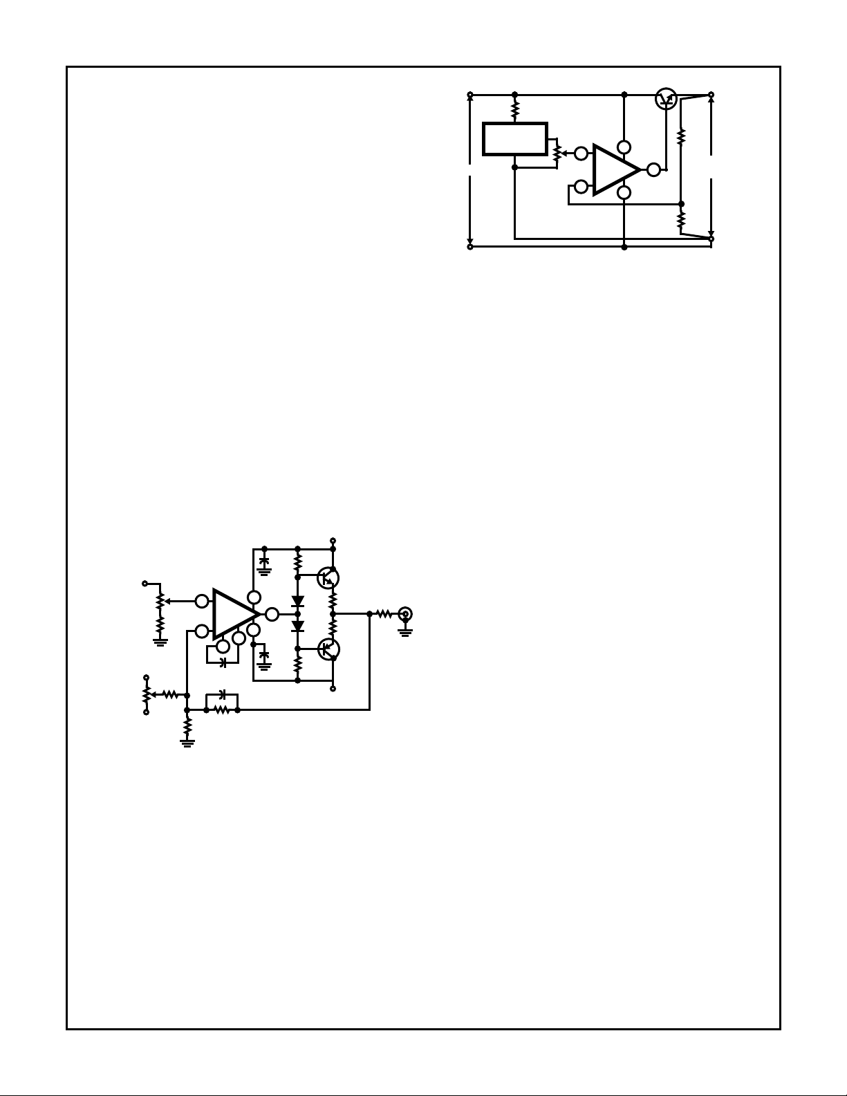
Figure 13 shows a sweeping generator. Three CA3140s are
used in this circuit. One CA3140 is used as an integrator, a
second device is used as a hysteresis switch that determines the starting and stopping points of the sweep. A third
CA3140 is used as a logarithmic shaping network for the log
function. Rates and slopes, as well as sawtooth, triangle,
and logarithmic sweeps are generated by this circuit.
Wideband Output Amplifier
Figure 14 shows a high slew rate, wideband amplifier
suitable for use as a 50Ω transmission line driver. This
circuit, when used in conjunction with the function generator
and sine wave shaper circuits shown in Figures 10 and 12
provides 18V
output open circuited, or 9V
P-P
P-P
output
when terminated in 50Ω. The slew rate required of this
amplifier is 28V/µs (18V
SIGNAL
LEVEL
ADJUSTMENT
2.5kΩ
200Ω
OUTPUT
DC LEVEL
ADJUSTMENT
+15V
3kΩ
-15V
200Ω
FIGURE 14. WIDEBAND OUTPUT AMPLIFIER
x π x 0.5MHz).
P-P
+
3
CA3140
-
2
8
1
2.4pF
2pF
1.8kΩ
+15V
+
-
7
4
-
+
NOMINAL BANDWIDTH = 10MHz
50µF
25V
6
50µF
25V
2.2
kΩ
1N914
1N914
2.2
kΩ
2N3053
2.7Ω
2.7Ω
2N4037
-15V
t
= 35ns
r
51Ω
2W
OUT
Power Supplies
High input impedance, common mode capability down to the
negative supply and high output drive current capability are
key factors in the design of wide range output voltage
supplies that use a single input voltage to provide a
regulated output voltage that can be adjusted from
essentially 0V to 24V.
Unlike many regulator systems using comparators having a
bipolar transistor input stage, a high impedance reference
voltage divider from a single supply can be used in
connection with the CA3140 (see Figure 15).
FIGURE 15. B ASIC SINGLE SUPPLY VOLTA GE REGULA T OR
SHOWING VOLTAGE FOLLOWER CONFIGURATION
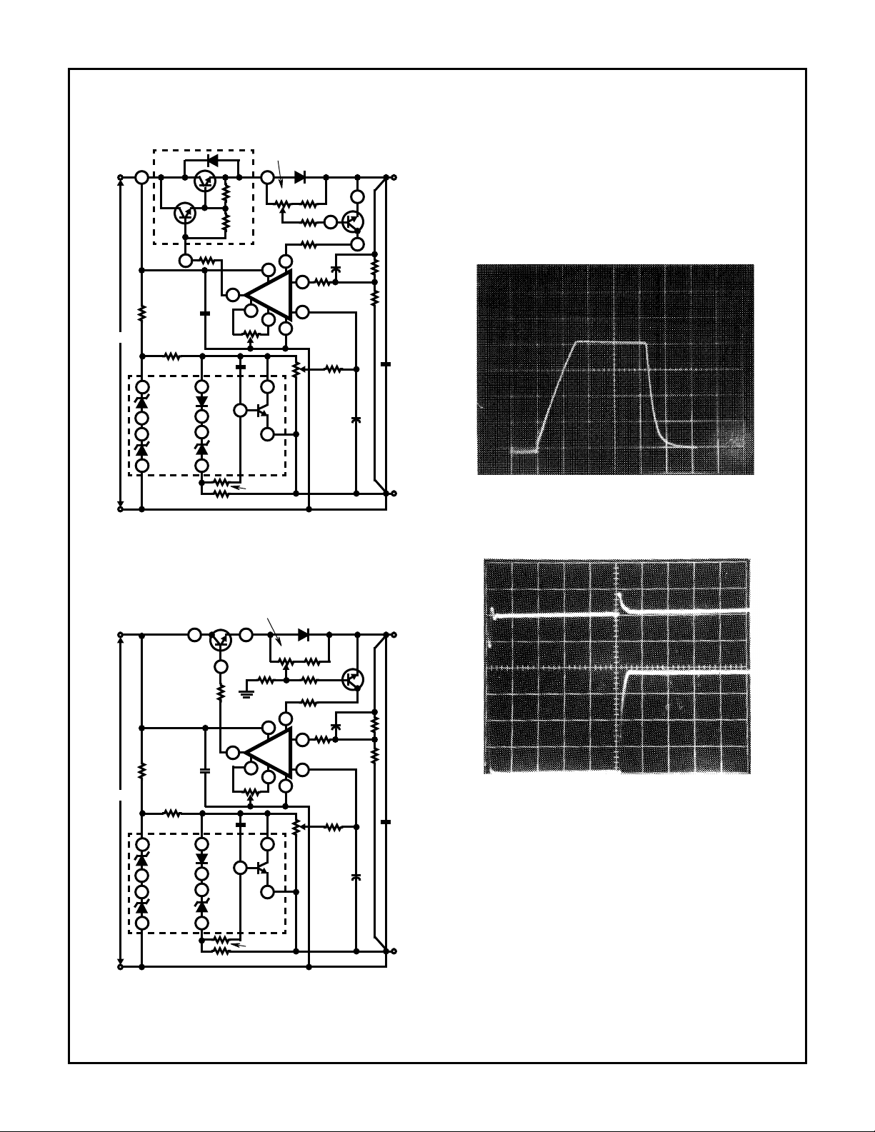
Essentially, the regulators, shown in Figures 16 and 17, are
connected as non inverting power operational amplifiers with
a gain of 3.2. An 8V reference input yields a maximum output voltage slightly greater than 25V. As a voltage follower,
when the reference input goes to 0V the output will be 0V.
Because the offset voltage is also multiplied by the 3.2 gain
factor, a potentiometer is needed to null the offset voltage.
Series pass transistors with high I
levels will also pre-
CBO
vent the output voltage from reaching zero because there is
a finite voltage drop (V
) across the output of the
CESAT
CA3140 (see Figure 2). This saturation voltage level may
indeed set the lowest voltage obtainable.
The high impedance presented by Terminal 8 is advantageous in effecting current limiting. Thus, only a small signal
transistor is required for the current-limit sensing amplifier.
Resistive decoupling is provided for this transistor to minimize damage to it or the CA3140 in the event of unusual
input or output transients on the supply rail.
Figures 16 and 17, show circuits in which a D2201 high
speed diode is used for the current sensor. This diode was
chosen for its slightly higher forward voltage drop characteristic, thus giving greater sensitivity. It must be emphasized
that heat sinking of this diode is essential to minimize variation of the current trip point due to internal heating of the
diode. That is, 1A at 1V forward drop represents one watt
which can result in significant regenerative changes in the
current trip point as the diode temperature rises. Placing the
small signal reference amplifier in the proximity of the current
sensing diode also helps minimize the variability in the trip
level due to the negative temperature coefficient of the
diode. In spite of those limitations, the current limiting point
can easily be adjusted over the range from 10mA to 1A with
a single adjustment potentiometer. If the temperature stability of the current limiting system is a serious consideration,
the more usual current sampling resistor type of circuitry
should be employed.
A power Darlington transistor (in a metal can with heatsink), is
used as the series pass element for the conventional current limiting system, Figure 16, because high power Darlington dissipation will be encountered at low output voltage and high currents.
A small heat sink VERSAWATT transistor is used as the
series pass element in the fold back current system, Figure
17, since dissipation levels will only approach 10W. In this
system, the D2201 diode is used for current sampling. Fold-
3-90
Page 13
CA3140, CA3140A
back is provided by the 3kΩ and 100kΩ divider network connected to the base of the current sensing transistor.
2N6385
POWER DARLINGTON
+30V
3
100Ω
1
+
10µF
2.7kΩ
INPUT
2.2kΩ
11
10
9
7
8
6
HUM AND NOISE OUTPUT <200µV
(MEASUREMENT BANDWIDTH~10MHz)
LINE REGULATION 0.1%/V
-
2
1
3
5
4
62kΩ
75Ω
3kΩ
6
100kΩ
+
-
12
CURRENT
LIMITING
ADJUST
2
7
CA3140
5
1
5µF
14
13
CA3086
1kΩ
RMS
D2201
1kΩ 1kΩ
1kΩ
2
2N2102
1kΩ
8
4
50kΩ
(NO LOAD TO FULL LOAD)
180kΩ
56pF
2
1kΩ
3
VOLTAGE
ADJUST
100kΩ
0.01µF
LOAD REGULATION
<0.02%
OUTPUT
0.1 ⇒ 24V
AT 1A
1
3
82kΩ
+
-
250µF
Both regulators provide better than 0.02% load regulation.
Because there is constant loop gain at all voltage settings, the
regulation also remains constant. Line regulation is 0.1% per
volt. Hum and noise voltage is less than 200µV as read with a
meter having a 10MHz bandwidth.
Figure 18A shows the turn ON and turn OFF characteristics
of both regulators. The slow turn on rise is due to the slow
rate of rise of the reference voltage. Figure 18B shows the
transient response of the regulator with the switching of a
20Ω load at 20V output.
5V/Div., 1s/Div.
FIGURE 18A. SUPPLY TURN-ON AND TURNOFF
CHARACTERISTICS
FIGURE 16. REGULATED POWER SUPPLY
“FOLDBACK” CURRENT
LIMITER
10µF
2
100kΩ
1
3
5
4
2N5294
1
+
-
2
62kΩ
3
6
100kΩ
+
-
12
+30V
2.7kΩ
INPUT
2.2kΩ
11
10
9
7
8
6
HUM AND NOISE OUTPUT <200µV
(MEASUREMENT BANDWIDTH~10MHz)
LINE REGULATION 0.1%/V
100kΩ
7
CA3140
5
1
5µF
14
13
CA3086
1kΩ
RMS
1kΩ 200Ω
8
4
50kΩ
OUTPUT ⇒ 0V TO 25V
25V AT 1A
“FOLDS BACK”
D2201
TO 40mA
3kΩ
2N2102
1kΩ
180kΩ
56pF
2
1kΩ
3
(NO LOAD TO FULL LOAD)
82kΩ
VOLTAGE
ADJUST
100kΩ
0.01µF
LOAD REGULATION
<0.02%
+
250µF
-
FIGURE 17. REGULATED POWER SUPPL Y WITH “FOLDB ACK”
CURRENT LIMITING
Top Trace: Output Voltage;
200mV/Div., 5µs/Div.
Bottom Trace: Collector of load switching transistor, load = 1A;
5V/Div., 5µs/Div.
FIGURE 18B. TRANSIENT RESPONSE
FIGURE 18. WAVEFORMS OF D YNAMIC CHARA CTERISTICS
OF POWER SUPPLY CURRENTS SHOWN IN
FIGURES 16 AND 17
Tone Control Circuits
High slew rate, wide bandwidth, high output voltage
capability and high input impedance are all characteristics
required of tone control amplifiers. Two tone control circuits
that exploit these characteristics of the CA3140 are shown in
Figures 19 and 20.
3-91
Page 14
CA3140, CA3140A
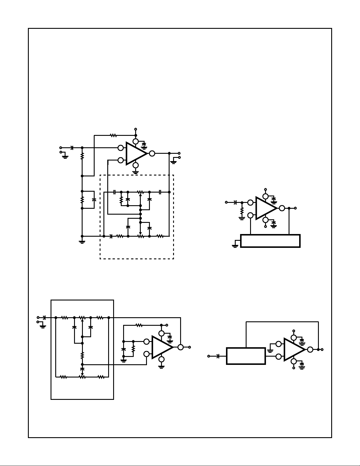
The first circuit, shown in Figure 20, is the Baxandall tone
control circuit which provides unity gain at midband and uses
standard linear potentiometers. The high input impedance of
the CA3140 makes possible the use of low-cost, low-value,
small size capacitors, as well as reduced load of the driving
stage.
Bass treble boost and cut are ±15dB at 100Hz and 10kHz,
respectively. Full peak-to-peak output is available up to at
least 20kHz due to the high slew rate of the CA3140. The
amplifier gain is 3dB down from its “flat” position at 70kHz.
FOR SINGLE SUPPLY
+30V
7
4
200kΩ
(LINEAR)
100
pF
0.1µF
6
100pF
0.0022µF
100kΩ
+
3
CA3140
-
2
10kΩ 1MΩ
CCW (LOG)
BOOST BASS CUT
TONE CONTROL NETWORK
0.005µF
5.1
MΩ
2.2MΩ
0.1
µF
2.2MΩ
BOOST TREBLE CUT
0.012µF 0.001µF
18kΩ
0.022µF
2µF
- +
Figure 19 shows another tone control circuit with similar
boost and cut specifications. The wideband gain of this circuit is equal to the ultimate boost or cut plus one, which in
this case is a gain of eleven. For 20dB boost and cut, the
input loading of this circuit is essentially equal to the value of
the resistance from Terminal No. 3 to ground. A detailed
analysis of this circuit is given in “An IC Operational
Transconductance Amplifier (OTA) With Power Capability” by
L. Kaplan and H. Wittlinger, IEEE Transactions on Broadcast
and Television Receivers, Vol. BTR-18, No. 3, August, 1972.
NOTES:
5. 20dB Flat Position Gain.
6. ±15dB Bass and Treble Boost and Cut
at 100Hz and 10kHz, respectively.
7. 25V
8. -3dB at 24kHz from 1kHz reference.
output at 20kHz.
P-P
0.005µF
5.1MΩ
FOR DUAL SUPPLIES
+15V
7
+
3
CA3140
-
2
-15V
TONE CONTROL NETWORK
0.1µF
6
4
0.1µF
0.047µF
FIGURE 19. TONE CONTROL CIRCUIT USING CA3130 SERIES (20dB MIDBAND GAIN)
FOR SINGLE SUPPLY
BOOST BASS CUT
(LINEAR)
240kΩ 5MΩ
750
pF
51kΩ 5MΩ
(LINEAR)
BOOST TREBLE CUT
TONE CONTROL NETWORK
240kΩ
750
pF
2.2MΩ
20pF
51kΩ
FIGURE 20. BAXANDALL TONE CONTROL CIRCUIT USING CA3140 SERIES
0.1
µF
2.2MΩ
2.2
MΩ
FOR DUAL SUPPLIES
TONE CONTROL
NETWORK
3
2
3
2
+32V
7
+
CA3140
-
4
0.1
µF
6
0.047µF
NOTES:
9. ±15dB Bass and Treble Boost and Cut at 100Hz and 10kHz, Respectively.
10. 25V
Output at 20kHz.
P-P
11. -3dB at 70kHz from 1kHz Reference.
12. 0dB Flat Position Gain.
+15V
7
+
CA3140
-
4
-15V
0.1µF
6
0.1µF
3-92
Page 15
CA3140, CA3140A
Wien Bridge Oscillator
Another application of the CA3140 that makes excellent use
of its high input impedance, high slew rate, and high voltage
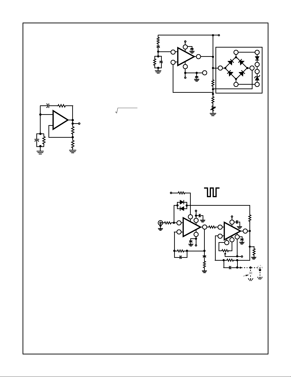
qualities is the Wien Bridge sine wave oscillator. A basic Wien
Bridge oscillator is shown in Figure 21. When R
and C
= C2 = C, the frequency equation reduces to the
1
= R2 = R
1
familiar f = 1/(2πRC) and the gain required for oscillation,
A
is equal to 3. Note that if C2 is increased by a factor of
OSC
four and R
is reduced by a factor of four, the gain required
2
for oscillation becomes 1.5, thus permitting a potentially
higher operating frequency closer to the gain bandwidth
product of the CA3140.
R
C
C
1
R
2
2
+
-
1
OUTPUT
R
F
R
S
NOTES:
f
A
OSC
A
CL
------------------------------------------ -=
2π R
1
1
1
1C1R2C2
C
1
------ -
C
2
R
F
------- -+=
R
S
R
2
------ -++=
R
1
FIGURE 21. BASIC WIEN BRIDGE OSCILLATOR CIRCUIT
USING AN OPERATIONAL AMPLIFIER
Oscillator stabilization takes on many forms. It must be
precisely set, otherwise the amplitude will either diminish or
reach some form of limiting with high levels of distortion. The
element, R
, is commonly replaced with some variable
S
resistance element. Thus, through some control means, the
value of R
is adjusted to maintain constant oscillator
S
output. A FET channel resistance, a thermistor, a lamp bulb,
or other device whose resistance increases as the output
amplitude is increased are a few of the elements often
utilized.
Figure 22 shows another means of stabilizing the oscillator
with a zener diode shunting the feedback resistor (R
of
F
Figure 21). As the output signal amplitude increases, the
zener diode impedance decreases resulting in more
feedback with consequent reduction in gain; thus stabilizing
the amplitude of the output signal. Furthermore, this
combination of a monolithic zener diode and bridge rectifier
circuit tends to provide a zero temperature coefficient for this
regulating system. Because this bridge rectifier system has
no time constant, i.e., thermal time constant for the lamp
bulb, and RC time constant for filters often used in detector
networks, there is no lower frequency limit. For example,
with 1µF polycarbonate capacitors and 22MΩ for the
frequency determining network, the operating frequency is
0.007Hz.
As the frequency is increased, the output amplitude must be
reduced to prevent the output signal from becoming slewrate limited. An output frequency of 180kHz will reach a slew
rate of approximately 9V/µs when its amplitude is 16V
P-P
.
OUTPUT
TO 22V
19V
C
2
R
1
R1 = R2 = R
3
2
+15V
7
+
CA3140
-
4
-15V
R
2
1000pF
C
1
1000
pF
50Hz, R = 3.3MΩ
100Hz, R = 1.6MΩ
1kHz, R = 160MΩ
10kHz, R = 16MΩ
0.1µF
6
SUBSTRATE
OF CA3019
0.1µF
7
0.1µF
7.5kΩ
3.6kΩ
500Ω
P-P
THD <0.3%
CA3109
DIODE
ARRAY
6
P-P
8
2
5 4
9
1
3
30kHz, R = 5.1MΩ
FIGURE 22. WIEN BRIDGE OSCILLATOR CIRCUIT USING
CA3140
Simple Sample-and-Hold System
Figure 23 shows a very simple sample-and-hold system
using the CA3140 as the readout amplifier for the storage
capacitor. The CA3080A serves as both input buffer
amplifier and low feed-through transmission switch (see
Note 13). System offset nulling is accomplished with the
CA3140 via its offset nulling terminals. A typical simulated
load of 2kΩ and 30pF is shown in the schematic.
5
0
+15V
7
6
4
-15V
200pF
400Ω
INPUT
STROBE
2kΩ
30kΩ
1N914
1N914
3
2
0.1µF
2kΩ
200pF
+
CA3080A
-
FIGURE 23. SAMPLE AND HOLD CIRCUIT
In this circuit, the storage compensation capacitance (C
SAMPLE
HOLD-15
3
2
100kΩ
C
1
SIMULATED LOAD
NOT REQUIRED
+15V
7
+
CA3140
-
1
5
2kΩ
0.1µF
0.1µF
4
-15V
30pF
6
0.1
µF
3.5kΩ
2kΩ
) is
1
only 200pF. Larger value capacitors provide longer “hold”
periods but with slower slew rates. The slew rate is:
dv
I
------
--- - 0.5mA 200pF⁄ 2.5V µs⁄== =
dt
C
NOTE:
13. AN6668 “Applications of the CA3080 and CA 3080A High Performance Operational Transconductance Amplifiers”.
3-93
Page 16
CA3140, CA3140A
Pulse “droop” during the hold interval is 170pA/200pF which is
0.85µV/µs; (i.e., 170pA/200pF). In this case, 170pA represents
the typical leakage current of the CA3080A when strobed off. If
C
were increased to 2000pF, the “hold-droop” rate will
1
decrease to 0.085µV/µs, but the slew rate would decrease to
0.25V/µs. The parallel diode network connected between
Terminal 3 of the CA3080A and Terminal 6 of the CA3140
prevents large input signal feedthrough across the input
terminals of the CA3080A to the 200pF storage capacitor when
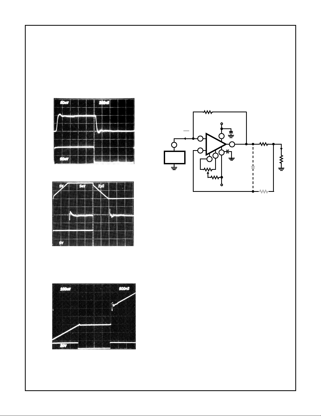
the CA3080A is strobed off. Figure 24 shows dynamic
characteristic wavef o rms of this sample-and-hold system.
Top Trace: Output; 50mV/Div., 200ns/Div.
Bottom Trace: Input; 50mV/Div., 200ns/Div.
Current Amplifier
The low input terminal current needed to drive the CA3140
makes it ideal for use in current amplifier applications such
as the one shown in Figure 25 (see Note 14). In this circuit,
low current is supplied at the input potential as the power
supply to load resistor R
the multiplication factor R
. This load current is increased by
L
, when the load current is mon-
2/R1
itored by the power supply meter M. Thus, if the load current
is 100nA, with values shown, the load current presented to
the supply will be 100µA; a much easier current to measure
in many systems.
R
1
10kΩ
+15V
R
2
I
x
L
M
POWER
SUPPLY
R
1
3
+
CA3140
-
2
1
5
100kΩ
4.3kΩ
-15V
0.1µF
7
6
0.1µF
4
R
2
10MΩ
I
L
R
L
Top Trace: Output Signal; 5V/Div, 2µs/Div.
Center Trace: Difference of Input and Output Signals through
Tektronix Amplifier 7A13; 5mV/Div., 2µs/Div.
Bottom Trace: Input Signal; 5V/Div., 2µs/Div.
LARGE SIGNAL RESPONSE AND SETTLING TIME
SAMPLING RESPONSE
Top Trace: Output; 100mV/Div., 500ns/Div.
Bottom Trace: Input; 20V/Div., 500ns/Div.
FIGURE 24. SAMPLE AND HOLD SYSTEM DYNAMIC
CHARACTERISTICS WAVEFORMS
FIGURE 25. BASIC CURRENT AMPLIFIER FOR LOW CURRENT
MEASUREMENT SYSTEMS
Note that the input and output voltages are transferred at the
same potential and only the output current is multiplied by
the scale factor.
The dotted components show a method of decoupling the
circuit from the effects of high output load capacitance and
the potential oscillation in this situation. Essentially, the
necessary high frequency feedback is provided by the
capacitor with the dotted series resistor providing load
decoupling.
Full Wave Rectifier
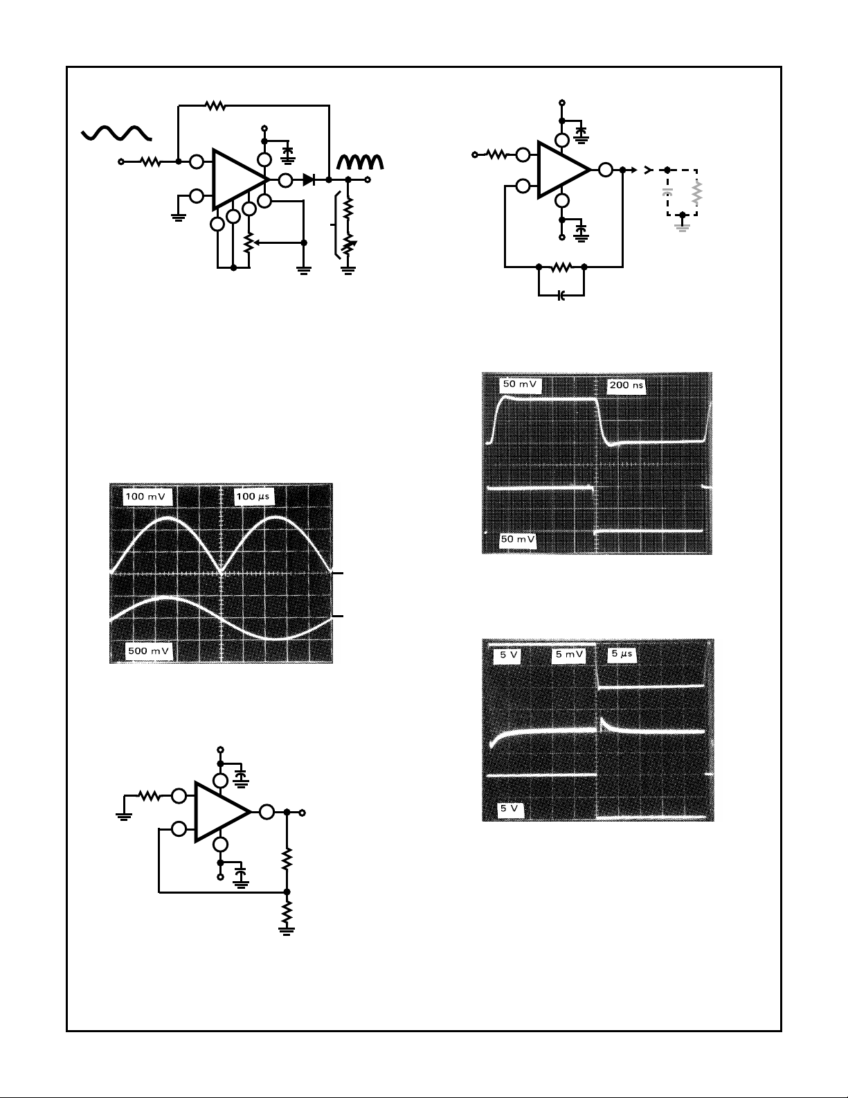
Figure 26 shows a single supply, absolute value, ideal fullwave rectifier with associated waveforms. During positive
excursions, the input signal is fed through the feedback
network directly to the output. Simultaneously, the positive
excursion of the input signal also drives the output terminal
(No. 6) of the inverting amplifier in a negative going
excursion such that the 1N914 diode effectively disconnects
the amplifier from the signal path. During a negative going
excursion of the input signal, the CA3140 functions as a
normal inverting amplifier with a gain equal to -R
2/R1
. When
the equality of the two equations shown in Figure 26 is
satisfied, the full wave output is symmetrical.
NOTE:
14. “Operational Amplifiers Design and Applications”, J. G. Graeme,
McGraw-Hill Book Company, page 308, “Negative Immittance
Converter Circuits”.
3-94
Page 17
CA3140, CA3140A
R
2
5kΩ
R
1
10kΩ
R
GAIN
R
3
2
------ - X
R
1
XX2+
-----------------
=
1X–
FOR X 0.5
10kΩ
R
3
20V
P-P
Input BW (-3dB) = 290kHz, DC Output (Avg) = 3.2V
R
1
5kΩ
-------------- -
10kΩ
0.75
-----------
0.5
2
3
---------------------------- -===
R1R2R3+
R
------ -==
R
15kΩ==
-
CA3140
+
8
R
3
2
1
1
+15V
7
4
5
100kΩ
OFFSET
ADJUST
0.1µF
6
1N914
R
+15V
0.1µF
3
2
7
+
CA3140
-
4
-15V
2kΩ
0.05µF
6
0.1µF
SIMULATED
LOAD
100pF
BW (-3dB) = 4.5MHz
2kΩ
SR = 9V/µs
INPUT
10kΩ
3
PEAK
ADJUST
10kΩ
100kΩ
FIGURE 28A. TEST CIRCUIT
OUTPUT
0
INPUT
0
FIGURE 26. SINGLE SUPPLY, ABSOLUTE VALUE, IDEAL FULL
WAVE RECTIFIER WITH ASSOCIATED
WAVEFORMS
+15V
0.01µF
R
S
1MΩ
BW (-3dB) = 140kHz
TOTAL NOISE VOLTAGE
(REFERRED TO INPUT ) = 48µV (TYP)
7
3
+
CA3140
-
2
4
-15V
6
0.01µF
NOISE VOLTAGE
OUTPUT
30.1kΩ
1kΩ
FIGURE 27. TEST CIRCUIT AMPLIFIER (30dB GAIN) USED FOR
WIDEBAND NOISE MEASUREMENT
Top Trace: Output; 50mV/Div., 200ns/Div.
Bottom Trace: Input; 50mV/Div., 200ns/Div.
FIGURE 28B. SMALL SIGNAL RESPONSE
(Measurement made with Tektronix 7A13 differential amplifier.)
Top Trace: Output Signal; 5V/Div., 5µs/Div.
Center Trace: Difference Signal; 5mV/Div., 5µs/Div.
Bottom Trace: Input Signal; 5V/Div., 5µs/Div.
FIGURE 28C. INPUT-OUTPUT DIFFERENCE SIGNAL SHOWING
SETTLING TIME
FIGURE 28. SPLIT SUPPLY VOLTAGE FOLLOWER TEST
CIRCUIT AND ASSOCIATED WAVEFORMS
3-95
Page 18
Typical Performance Curves
CA3140, CA3140A
= 2kΩ
R
L
TA = -55oC
o
C
125
100
75
50
25
OPEN-LOOP VOLTAGE GAIN (dB)
0
0 5 10 15 20
SUPPLY VOLTAGE (V)
25
125oC
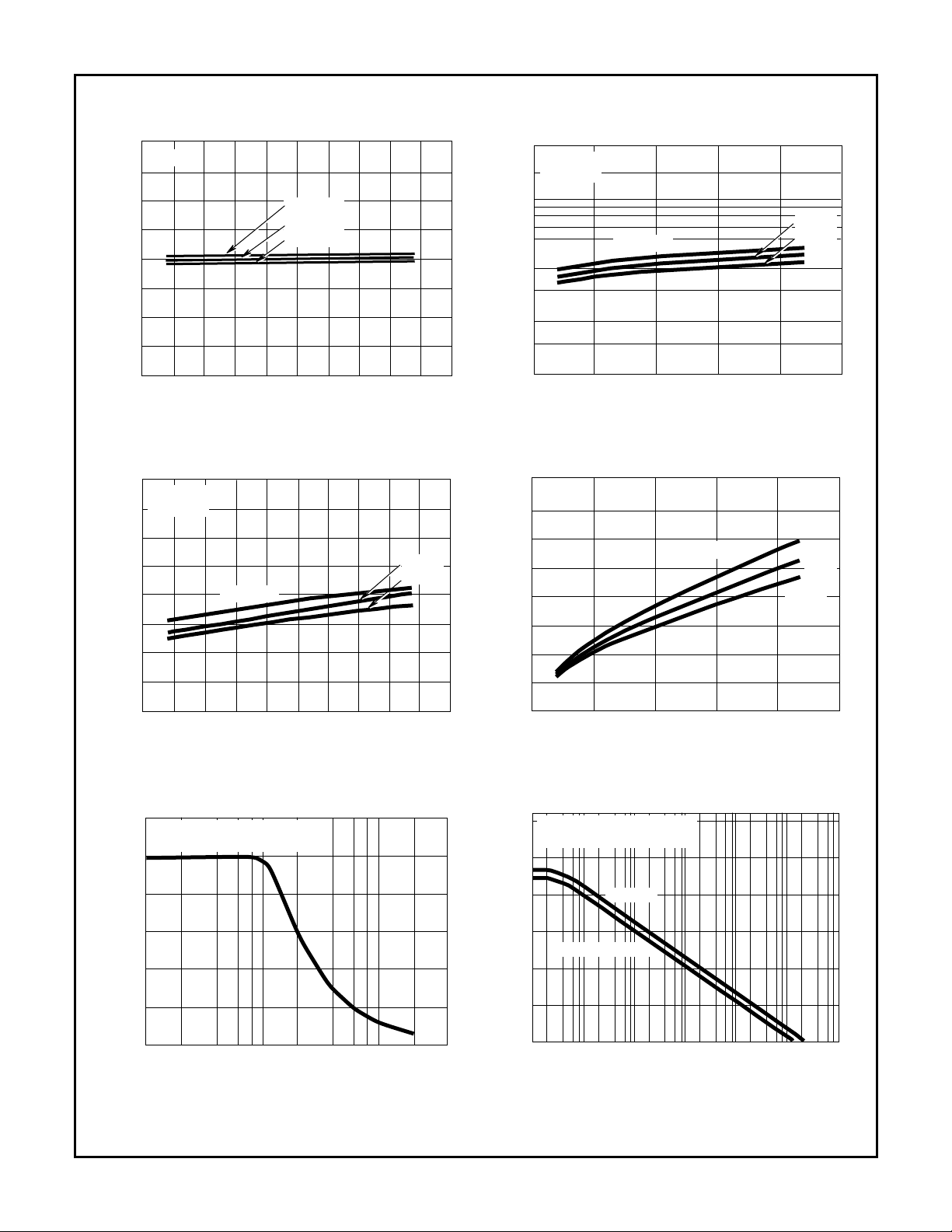
FIGURE 29. OPEN-LOOP VOLTAGE GAIN vs SUPPLY
VOLTAGE AND TEMPERATURE
= 2kΩ
R
L
C
= 100pF
L
20
15
TA = -55oC
o
C
25
125oC
20
= 2kΩ
R
L
C
= 100pF
L
10
TA = -55oC
GAIN BANDWIDTH PRODUCT (MHz)
1
25
0 5 10 15 20
SUPPLY VOLTAGE (V)
FIGURE 30. GAIN BANDWIDTH PRODUCT vs SUPPLY
VOLTAGE AND TEMPERATURE
= ∞
R
L
7
6
5
4
3
TA = -55oC
25
125oC
125oC
o
C
25oC
25
10
5
SLEW RATE (V/µs)
0
0
5101520
SUPPLY VOLTAGE (V)
FIGURE 31. SLEW RATE vs SUPPLY VOLTAGE AND
TEMPERATURE
SUPPLY VOLTAGE: VS = ±15V
T
= 25oC
A
25
)
P-P
20
15
10
OUTPUT SWING (V
5
0
10K 100K
FREQUENCY (Hz)
1M 4M
FIGURE 33. MAXIMUM OUTPUT VOLTAGE SWING vs
FREQUENCY
2
1
QUIESCENT SUPPLY CURRENT (mA)
0
25
0 5 10 15 20
SUPPLY VOLTAGE (V)
FIGURE 32. QUIESCENT SUPPLY CURRENT vs SUPPLY
VOLTAGE AND TEMPERATURE
120
SUPPLY VOLTAGE: VS = ±15V
TA = 25oC
100
80
60
40
20
COMMON-MODE REJECTION RATIO (dB)
0
10
CA3140, CA3140A
1
10
2
CA3140B
3
10
FREQUENCY (Hz)
4
10
5
10
FIGURE 34. COMMON MODE REJECTION RATIO vs FREQUENCY
25
6
10
7
10
3-96
Page 19
CA3140, CA3140A
Typical Performance Curves
1000
SUPPLY VOLTAGE: VS = ±15V
T
= 25oC
A
100
10
EQUIVALENT INPUT NOISE VOLT AGE (nV√Hz)
1
110
1102
FREQUENCY (Hz)
(Continued)
3
10
10
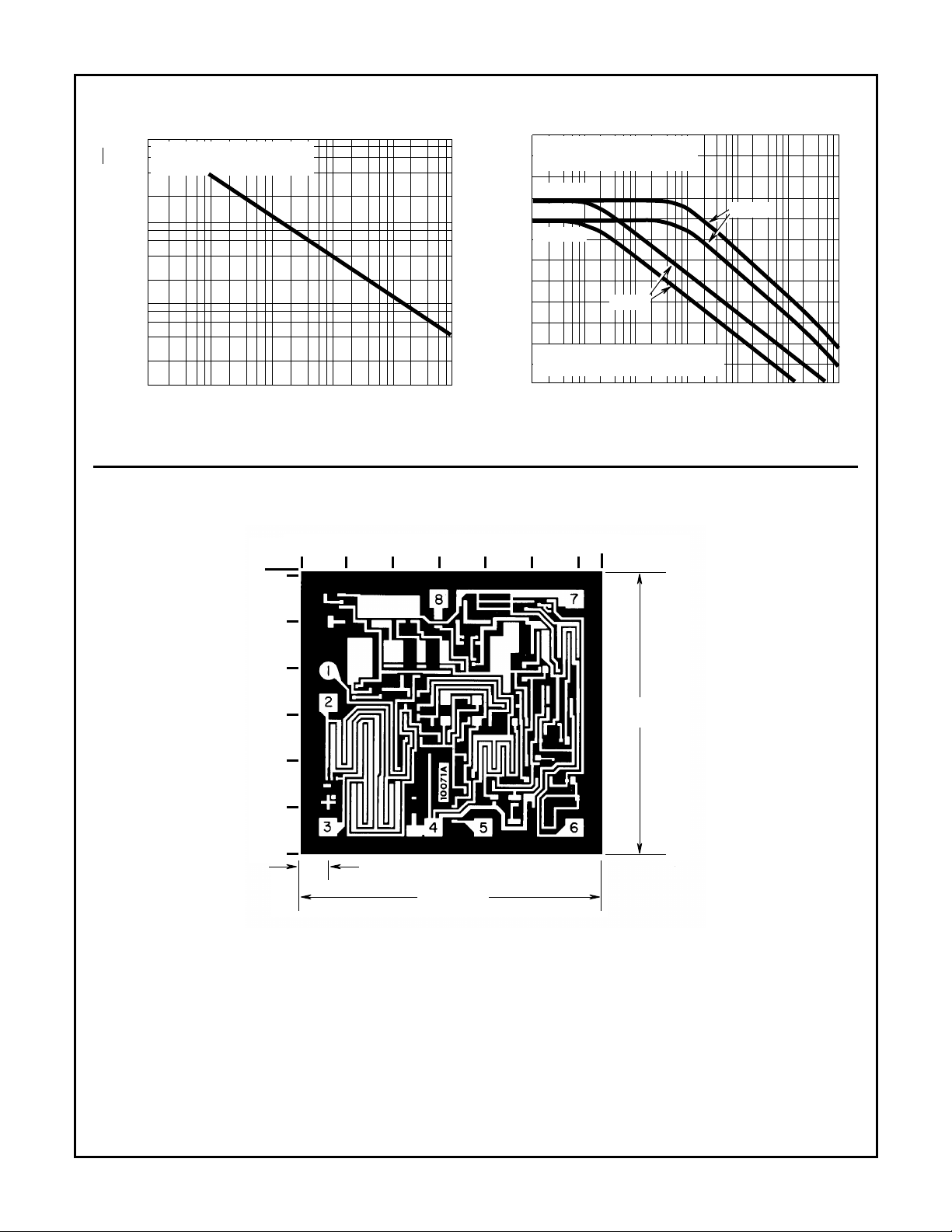
FIGURE 35. EQUIVALENT INPUT NOISE VOLTAGE vs
FREQUENCY
Metallization Mask Layout
0 60
61
60
SUPPLY VOLTAGE: VS = ±15V
T
= 25oC
A
100
CA3140B
CA3140
80
CA3140A
60
40
20
POWER SUPPLY REJECTION RATIO
(PSRR) = ∆V
POWER SUPPLY REJECTION RATIO (dB)
0
4
5
10
1
10
-PSRR
/∆V
IO
S
2
10
3
10
10
FREQUENCY (Hz)
+PSRR
4
5
10
6
10
7
10
FIGURE 36. POWER SUPPLY REJECTION RATIO vs FREQUENCY
5040302010
65
50
40
30
20
10
0
4-10
(0.102-0.254)
62-70
(1.575-1.778)
Dimensions in parenthesis are in millimeters and are derived
from the basic inch dimensions as indicated. Grid graduations
are in mils (10-3 inch).
The photographs and dimensions represent a chip when it is
part of the wafer. When the wafer is cut into chips, the cleavage
angles are 57o instead of 90ο with respect to the face of the
chip. Therefore, the isolated chip is actually 7 mils (0.17mm)
larger in both dimensions.
58-66
(1.473-1.676)
3-97
 Loading...