

Page 1
Semiconductor
CA3262A, CA3262
August 1997
Features
• Independent Over-Current Limiting On Each Output
• Independent Over-Temperature Limiting On Each Output
• Output Drivers Capable of Switching 700mA Load
• Inputs Compatible With TTL or 5V CMOS Logic
• Suitable For Resistive, Lamp or Inductive Loads
• Power-Frame Package Construction For Good Heat
Dissipation
• Operating Temperature Ranges
- CA3262A . . . . . . . . . . . . . . . . . . . . . . . -40
- CA3262 . . . . . . . . . . . . . . . . . . . . . . . . . -40
o
C to 125oC
o
C to 85oC
Applications System Applications
• Solenoids • Automotive
• Relays • Appliances
• Lamps • Industrial Controls
• Steppers • Robotics
• Small Motors
• Displays
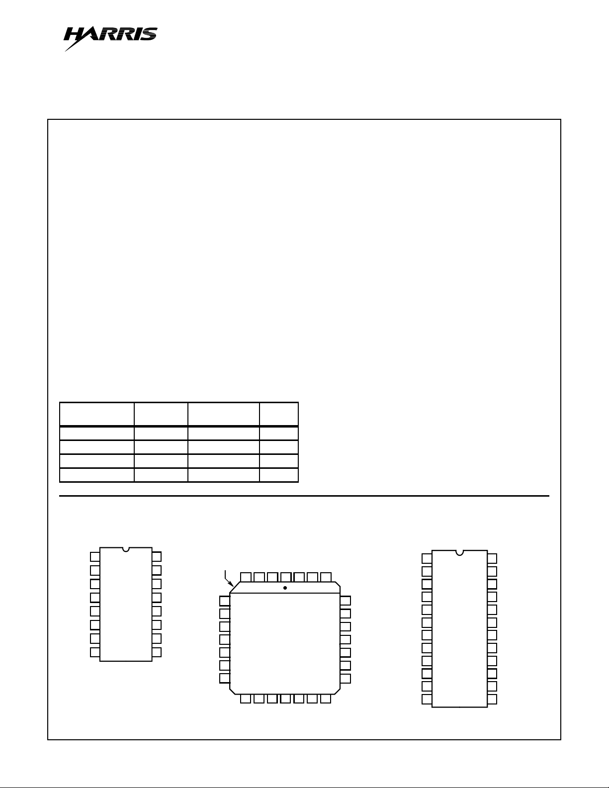
Ordering Information
TEMP.
PART NUMBER
CA3262E -40 to 85 16 Ld PDIP E16.3
CA3262AE -40 to 125 16 Ld PDIP E16.3
CA3262AQ -40 to 125 28 Ld PLCC N28.45
CA3262AM -40 to 125 24 Ld SOIC (W) M24.3
RANGE (oC) PACKAGE
PKG.
NO.
Quad-Gated, Inverting Power Drivers
Description
The CA3262 and CA3262A are used to interface low-level
logic to high current loads. Each Power Driver has four
inverting switches consisting of a non-inverting logic input
stage and an inverting low-side driver output stage. All inputs
are 5V TTL/CMOS logic compatible and have a common
Enable input. Each output device has independent current
limiting (I
over-load conditions. Steering diodes connected from each
output (in pairs) to the Clamp pins may be used in
conjunction with external zener diodes to protect the IC
against over-voltage tr ansients that result from inductive load
switching.
To allow for maximum heat transfer from the chip, all ground
pins on the DIP, PLCC and SOIC packages are directly
connected to the mounting pad of the chip. Integral heat
spreading lead frames directly connect the bond pads and
ground leads to conduct heat from the chip junction to the
PC Board for good heat dissipation.
The CA3262 and CA3262A can drive four incandescent
lamp loads without modulating their brilliance when the
“cold” lamps are energized. Outputs may be parallel
connected to drive high current loads. The maximum output
current of each output is determined by the over-current limiting threshold which is typically 1.2A but may be as low as
0.7A.
) and thermal limiting (T
LIM
) for protection from
LIM
Pinouts
CA3262, CA3262A (PDIP)
TOP VIEW
1
OUT A
CLAMP
CLAMP
CAUTION: These devices are sensitive to electrostatic discharge. Users should follow proper IC Handling Procedures.
Copyright
2
3
OUT B
4
GND
GND
5
OUT C
6
7
OUT D
8
© Harris Corporation 1997
16
15
14
13
12
11
10
9
IN A
IN B
ENABLE
GND
GND
V
CC
IN C
IN D
GND
GND
GND
GND
GND
GND
GND
INDEX
5
6
7
8
9
10
11
CA3262A (PLCC)
TOP VIEW
CLAMP
OUT A
OUT B
12 13 14 15 16 17 18
OUT C
CLAMP
NC
1234
NC
OUT D
IN A
IN D
IN B
IN C
1
ENABLE
262728
CC
V
OUT A
CLAMP
OUT B
GND
25
GND
24
GND
23
GND
22
21
GND
20
GND
19
GND
GND
GND
GND
GND
OUT C
CLAMP
OUT D
CA3262A (SOIC)
PRELIMINARY
1
2
3
4
NC
5
6
7
8
NC
9
10
11
12
TOP VIEW
24
IN A
23
IN B
22
ENABLE
21
NC
20
GND
19
GND
GND
18
GND
17
NC
16
V
15
IN C
14
IN D
13
File Number 1836.6
CC
Page 2
CA3262A, CA3262
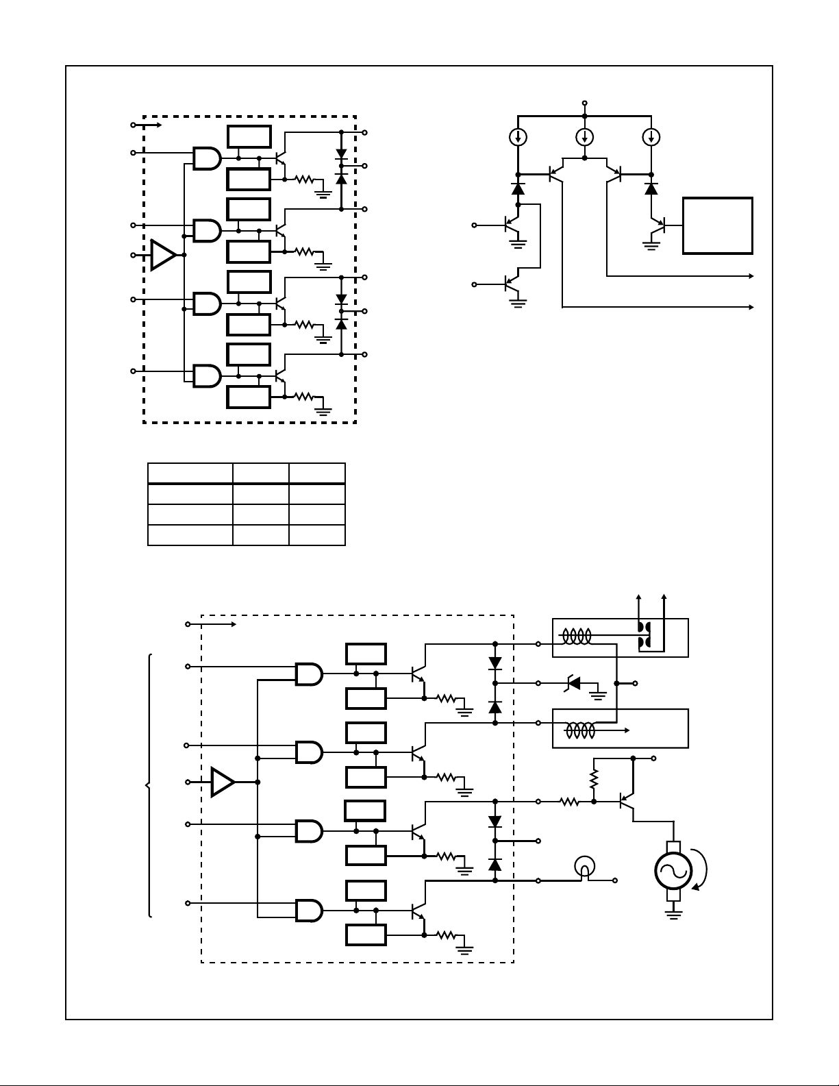
Functional Block Diagram
V
CC
IN D
IN C
ENABLE
IN B
IN A
V+
T
I
T
I
T
I
T
I
LIM
LIM
LIM
LIM
LIM
LIM
LIM
LIM
TRUTH TABLE (Each Output)
ENABLE IN OUT
HHL
HLH
LXH
H = High, L = Low, X = Don’t Care
OUT D
CLAMP
OUT C
OUT B
CLAMP
OUT A
V
CC
CONSTANT
CURRENT
SOURCES
REFERENCE
INPUT
ENABLE
TO SUBSEQUENT STAGES
VOLTAGE
FIGURE 1. CA3262A EQUIV ALENT SCHEMATIC OF ONE
INPUT STAGE
1.2V
TTL OR
CMOS
LOGIC
LEVEL
INPUTS
V
+5V P.S.
ENABLE
CC
IN D
IN C
IN B
IN A
V+
T
I
T
I
T
I
T
I
LIM
LIM
LIM
LIM
LIM
LIM
LIM
LIM
OUT D
CLAMP
OUT C
OUT B
CLAMP
OUT A
LAMP
RELAY
V
BATT
FIGURE 2. QUAD INVERTING POWER DRIVER (QDR) SHOWN WITH TYPICAL APPLICATION LOADS
V
BATT
SOLENOID
V
BATT
HIGH CURRENT
HIGH SIDE DR
MOTOR
2
Page 3
CA3262A, CA3262
Absolute Maximum Ratings Thermal Information
Logic Supply Voltage, VCC. . . . . . . . . . . . . . . . . . . . . . . . . . . . . . 7V
Logic Input Voltage, VIN. . . . . . . . . . . . . . . . . . . . . . . . . . . . . . . 15V
Output Voltage, V
Output Sustaining Voltage, V
. . . . . . . . . . . . . . . . . . . . . . . . . . . . . . . . . 60V
CEX
CE(SUS)
. . . . . . . . . . . . . . . . . . . . 40V
Output Transient Current . . . . . . . . . . . . . . . . . . . . . . . . . . (Note 1)
Output Load Current. . . . . . . . . . . . . . . . . . . . . . . . . . . . . . (Note 2)
Operating Conditions
Temperature Range
CA3262AE, CA3262AQ, CA3262AM . . . . . . . . . . -40oC to 125oC
CA3262E. . . . . . . . . . . . . . . . . . . . . . . . . . . . . . . . . -40oC to 85oC
CAUTION: Stresses above those listed in “Absolute Maximum Ratings” may cause permanent damage to the device. This is a stress only rating and operation
of the device at these or any other conditions above those indicated in the operational sections of this specification is not implied.
Thermal Resistance (Typical, Note 3) θJA (oC/W)
For PC Mount Without Added Copper Ground Area
CA3262E (PDIP) . . . . . . . . . . . . . . . . . . . . . . . . . 60
CA3262AE (PDIP) . . . . . . . . . . . . . . . . . . . . . . . . 60
CA3262AQ (PLCC) . . . . . . . . . . . . . . . . . . . . . . . 45
CA3262AM (SOIC) . . . . . . . . . . . . . . . . . . . . . . . 60
For PC Mount With 2 sq. in. of Added Copper Ground Area
CA3262E (PDIP) . . . . . . . . . . . . . . . . . . . . . . . . . 40
CA3262AE (PDIP) . . . . . . . . . . . . . . . . . . . . . . . . 40
CA3262AQ (PLCC) . . . . . . . . . . . . . . . . . . . . . . . 36
CA3262AM (SOIC) . . . . . . . . . . . . . . . . . . . . . . . 36
See Maximum Power Dissipation vs Temperature curves, Figures
6A and 6B.
Maximum Junction Temperature . . . . . . . . . . . . . . . . . . . . . . . 150oC
Maximum Storage Temperature Range . . . . . . . . . .-65oC to 150oC
Maximum Lead Temperature (Soldering 10s) . . . . . . . . . . . . . 265oC
Electrical Specifications V
= 5.5V, TA = -40oC to 125oC for CA3262A and VCC = 5.5V, TA = -40oC to 85oC for CA3262
CC
Unless Otherwise Specified
PARAMETER SYMBOL TEST CONDITIONS
Output Leakage Current I
Output Sustaining
V
CEX
CE(SUS)
VCE = 60V, V
Note 5 40 - - 40 - - V
Voltage
Collector Emitter
Saturation Voltage
(See Figures 4B and 5B)
V
CE(SAT)VIN
= 2V, VCC = 4.75V
IC = 100mA - - 0.25 - 0.05 0.15 V
IC = 200mA - ----0.2V
IC = 300mA - ----0.25 V
IC = 400mA - - 0.4 - 0.2 0.3 V
IC = 500mA - ----0.4V
IC = 600mA - - 0.6 - - 0.5 V
IC = 700mA, TA = -40oC - - 0.6 - - 0.5 V
Input Low Voltage V
Input High Voltage V
Input Low Current I
Input High Current I
IL
IH
VIN = 0.8V - - 10 - 0.75 10 µA
IL
VIN = V
IH
ENABLE
IC = 600mA
Supply Current,
All Outputs ON,
(See Figures 4A and 5A)
Supply Current, All
Outputs OFF,
I
CC(ON)VIN
I
CC(OFF)
= 2V, V
I
= 250mA, I
OUTA
I
= 250mA, I
OUTC
VIN = 0V
(See Figures 4A and 5A)
Clamp Diode Leakage
Current
Clamp Diode Forward
Voltage,
(See Figures 4D and 5D)
Turn-On Delay,
t
PHL
I
R
VR = 60V
V
IF = 1A, VIN = 0V - - 1.7 - - 1.7 V
F
IF = 1.5A, VIN = 0V
, t
PLHIOUT
= 500mA - - 8 - - 8 µs
(See Figures 4C and 5C)
Over Current Limiting I
LIM
V
= 2V, VIN = 5.5V,
OUT
V
ENABLE
= 5.5V
DESIGN PARAMETERS
Over Temperature Limiting
T
LIM
(Junction Temperature)
ENABLE
= 5.5V,
ENABLE
CA3262 CA3262A
= 0.8V - - 100 - 0.6 50 µA
- - 0.8 - - 0.8 V
2--2- -V
- - 10 - - 10 µA
= 5.5V,
OUTB
OUTD
= 250mA,
= 250mA
- - 70 - (Note 4) 55 mA
- - 5 - (Note 4) 5 mA
- - 100 - - 50 µA
- - 2.1 - - 2.1 V
0.7 - (Note 1) 0.7 - (Note 1) A
- 155 - - 155 -
UNITSMIN TYP MAX MIN TYP MAX
o
C
3
Page 4

CA3262A, CA3262
Electrical Specifications V
PARAMETER SYMBOL TEST CONDITIONS
Input Capacitance, Input
Enable Capacitance
NOTES:
1. The CA3262 and CA3262A have on-chip limiting f or transient peak currents. Under short-circuit conditions with voltage applied to the collector
of the output transistor and with the output transistor turned ON, the current will increase to 1.2A, typical. Over-Current Limiting protects a short
circuit condition for a normal operating range of output supply voltage. During a short circuit condition, the output driver will shortly thereafter
(approx. 5ms) go into Over-Temperature Limiting. While Over-Current Limiting may range to peak currents greater than 2A, each output will
typically withstand a direct short circuit up to supply voltage levels of 16V. Excessive dissipation before thermal limiting occurs may cause damage to the chip for supply voltages greater than 18V. The CA3262 and CA3262A are rated to withstand peak current, cold turn-on conditions of
#168 or #194 lamp loads.
2. The total DC current for the CA3262 and CA3262A with all 4 outputs ON should not exceed the total of (4 x 0.7A + Max. ICC) ~ 2.85A. This level
of current will significantly increase the chip temperature due to increased dissipation and may cause thermal shutdown in high ambient temperature conditions (See Absolute Maximum Ratings for Dissipation). Any one output may be allowed to exceed 0.7A but may be subject to
Over-Current Limiting above the I
3. Normal applications require a surface mount of the 28 lead PLCC and 24 lead SOIC packages on a PC Board. The PLCC , SOIC and PDIP
packages have pow er lead frame construction through the ground pins to conduct heat from the frame to the PC Board ground area. Thermal
resistance, θJA, is given for a surface mount of the 28 lead PLCC and the 24 lead SOIC pac kages on a 1 oz. copper PC board with minimal
ground area and with 2 square inches of ground area.
4. ICC varies with temperature. Typically, I
-40oC.
5. Tested with a s witched-off 500mA Load of 120mH (with 24Ω series resistance), V
with an external zener diode.
= 5.5V, TA = -40oC to 125oC for CA3262A and VCC = 5.5V, TA = -40oC to 85oC for CA3262
CC
Unless Otherwise Specified (Continued)
CA3262 CA3262A
C
IN
C
EN
min. limit of 0.7A. As a practical limit, no single output should be loaded to more than 1A (Max).
LIM
is 18mA at 125oC and 41mA at -40oC. Typically, I
CC(ON)
-
-
-
-
= 12V and the outputs (VCE) clamped to +40V maximum
BA TT
--3 -pF
- - 4.4 - pF
is 2.2mA at 125oC and 1.2mA at
CC(OFF)
UNITSMIN TYP MAX MIN TYP MAX
Applications
Typical circuit configurations for applying the CA3262 and
CA3262A are shown in the application circuit of Figure 2. To
their rated capabilities, both circuits can be used to drive inductive, resistive and lamp loads. The CA3262A has a lower V
than the CA3262 and is rated for 125oC ambient temperature
applications. The CA3262 data sheet rating is 85
o
C. Otherwise,
the protection features described apply to both the CA3262 and
CA3262A.
The maximum voltage for full load current switching is the
output sustaining voltage, V
CE(SUS)
which should not exceed
40V. To provide a means of over-voltage protection, on-chip
steering diodes are connected from each output to one of two
CLAMP pins. Over-voltage pulses may be generated from
inductive load switching and must be clamped or limited to a
peak voltage less than V
CE(SUS)
. To limit an inductive voltage
pulse, a zener diode should be connected to the appropriate
CLAMP pin. When the voltage pulse exceeds the zener threshold, the excess energy is dumped to ground via the on-chip
steering diode and the external zener diode.
The on-chip diodes may be used in a free-wheeling mode by
connecting the CLAMP pins to an external clamp supply
voltage. Zener diode clamp protection is preferred over the
power supply clamp option, primarily because the power
supplies may be subject to large transient changes; including
turn-ON and turn-OFF conditions where non-tracking conditions
between supplies could allow forward conduction through the
steering diodes. For all transient conditions of either method, the
clamp voltage should greater than the maximum supply voltage
of the switching outputs and less than V
CE(SUS)
.
SAT
Note that the rate of change of the output current during load
switching is fast. Therefore, even small values of inductance,
including the inductance of a few meters of hook-up wire to
the load circuit, can generate voltage spikes of considerable
amplitude at the output terminals and may require clamping
to protect the device ratings.
Current-limiting is provided as protection for shorted or overloaded output conditions. Voltage is sampled across a small
metal resistor in the emitter of each output stage. When the voltage exceeds a preset comparator level, drive is reduced to the
output. Current limiting is sustained unless thermal conditions
exceed the preset thermal shutdown temperature of 155
o
C.
If an output is shorted, the remaining three outputs will
continue to function normally unless the continued heat
spreading is sufficient to raise the junction temperature at any
other output to a level greater than 155
o
C. High ambient temperature conditions may allow this to happen. The degree of
interaction is minimized at chip layout design by separating
the output devices, each to a separate corner of the chip.
As noted, the thermal resistance values of the PDIP, PLCC
and SOIC packages are improved by direct connection of
the leads to the chip mounting pad. For a normal PC Board
application, the thermal resistance coefficient for each package can be significantly lowered by increasing ground copper area on the PC board next to the ground pins of the IC.
4
Page 5

CA3262A, CA3262
I
B
CURRENT
AMPLIFIER
CURRENT
SENSE
TEMP.
SENSE
BANDGAP
VOLT. REF.
FIGURE 3. EACH OUTPUT PO WER DRIVER IS A COMPOSITE CIRCUIT WITH OVER-TEMPERA TURE SENSE FOR THERMAL
LIMITING AND OVER-CURRENT SENSE TO PROVIDE CURRENT LIMITING
Typical Performance Curves
80
SUPPLY VOLTAGE (VCC) = 5.5V
70
SUPPLY VOLTAGE (VCC) = 4.75V
0.7
60
50
VIN = 2V, I
40
30
SUPPLY CURRENT (mA)
20
10
0
-40 -20 0 20 40 60 80 100 120
THERMAL SHUTDOWN
VIN = 0V, I
AMBIENT TEMPERATURE (oC)
OUT
= 250mA (EACH)
OUT
= 0mA
140
FIGURE 4A. TYPICAL SUPPLY CURRENT (PIN 11)
CHARACTERISTICS
4
3
t
PHL
V
2
1
PROPAGATION DELAY TIME (µs)
0
-40 -20 0 20 40 60 80 100 120
IN
9, 10, 15, 16
(16) (17) (27) (28)
V
OUT
1, 3, 6, 8
(2) (4) (12) (14)
AMBIENT TEMPERATURE (
50% 50%
t
PHL
(ON)
t
PLH
50%
o
C)
t
PLH
(OFF)
50%
140
FIGURE 4C. TYPICAL PROPAGATION DELAY TIME CHARAC-
TERISTICS
FIGURE 4. TYPICAL CHARACTERISTICS OF THE CA3262E
0.6
0.5
IC = 700mA
0.4
0.3
0.2
COLLECTOR-TO-EMITTER
SATURATION VOLTAGE (V)
0.1
-40 -20 0 20 40 60 80 100 120
AMBIENT TEMPERATURE (
IC = 600mA
o
C)
140
FIGURE 4B. TYPICAL COLLECTOR-TO-EMITTER SATURATION
VOLTAGE CHARACTERISTICS IN QUAD-GATED
INVERTING POWER DRIVER OUTPUT
4
3
2
1
CLAMP DIODE FORWARD VOLTAGE (V)
0
-40 -20 0 20 40 60 80 100 120
IF = 1.5A
IF = 1A
AMBIENT TEMPERATURE (
o
C)
140
FIGURE 4D. TYPICAL CLAMP-DIODE FORWARD VOLTAGE
CHARACTERISTICS
5
Page 6

CA3262A, CA3262
Typical Performance Curves
80
SUPPLY VOLTAGE (VCC) = 5.5V
70
60
50
40
30
20
SUPPLY CURRENT (mA)
10
0
-40 -20 0 20 40 60 80 100 120 140
V
IN
I
OUT
AMBIENT TEMPERATURE (oC)
LOW
= 0mA
VIN HIGH
I
OUT
(Continued)
= 500mA (EACH)
FIGURE 5A. TYPICAL SUPPLY CURRENT (PIN 11)
CHARACTERISTICS
4
3
t
PHL
SUPPLY VOLTAGE (VCC) = 4.75
I
0.7
0.6
0.5
0.4
0.3
0.2
COLLECTOR-TO-EMITTER
SATURATION VOLTAGE (V)
0.1
= 600mA
OUT
-40 -20 0 20 40 60 80 100 120 140
AMBIENT TEMPERATURE (oC)
FIGURE 5B. TYPICAL COLLECTOR-TO-EMITTER SATURATION
VOLTAGE CHARACTERISTICS IN QUAD-GATED
INVERTING POWER DRIVER OUTPUTS
4
3
2
V
V
t
PHL
OUT
IN
(ON)
1
PROPAGATION DELAY TIME (µs)
0
9, 10, 15, 16
(16) (17) (27) (28)
1, 3, 6, 8
(2) (4) (12) (14)
-40 -20 0 20 40 60 80 100 120 140
AMBIENT TEMPERATURE (oC)
50%
50%
t
PLH
(OFF)
t
FIGURE 5C. TYPICAL PROPAGATION DELAY TIME
CHARACTERISTICS
FIGURE 5. TYPICAL CHARACTERISTICS OF THE CA3262AE AND CA3262AQ
2
1.5
1
PACKAGE DERATING WITHOUT HEAT SINK
0.5
1 - CA3262AQ (PLCC)
PACKAGE DISSIPATION (W)
2 - CA3262AE (PDIP), CA3262AM (SOIC)
0
-50 0 50 100 150
AMBIENT TEMPERATURE (
1
o
C)
FIGURE 6A. DISSIPATION RATING CHART FOR PLCC, PDIP
AND SOIC PACKAGES WITHOUT ADDITIONAL
HEAT SINKS
PLH
2
1
CLAMP DIODE FORW ARD VOLTAGE (V)
0
-40 -20 0 20 40 60 80 100 120 140
IF = 1.5A
IF = 1A
AMBIENT TEMPERATURE (
o
C)
FIGURE 5D. TYPICAL CLAMP-DIODE FORWARD VOLTAGE
CHARACTERISTICS
32
1.5
1
PACKAGE DERATING WITH 2 SQ INCHES OF
COPPPER PC BOARD HEAT SINK AREA
0.5
1 - CA3262AQ (PLCC)
PACKAGE DISSIPATION (W)
2 - CA3262AM (SOIC)
3 - CA3262AE (PDIP)
0
-50 0 50 100 150
AMBIENT TEMPERATURE (
1
o
C)
FIGURE 6B. DISSIPATION RATING CHART FOR PLCC, PDIP
AND SOIC PACKAGES WITH 2 SQ. IN. OF
COPPER PC BOARD HEAT SINKING
6
Page 7

CA3262A, CA3262
Dual-In-Line Plastic Packages (PDIP)
N
D1
-C-
E1
-B-
A1
A2
A
L
e
C
S
INDEX
AREA
BASE
PLANE
SEATING
PLANE
D1
B1
1 2 3 N/2
-AD
e
B
0.010 (0.25) C AMB
NOTES:
1. Controlling Dimensions: INCH. In case of conflict between
English and Metric dimensions, the inch dimensions control.
2. Dimensioning and tolerancing per ANSI Y14.5M-1982.
3. Symbols are defined in the “MO Series Symbol List” in Section
2.2 of Publication No. 95.
4. Dimensions A, A1 and L are measured with the package seated
in JEDEC seating plane gauge GS-3.
5. D, D1, and E1 dimensions do not include mold flash or protrusions. Mold flash or protrusions shall not exceed 0.010 inch
(0.25mm).
6. E and are measured with the leads constrained to be per-
e
pendicular to datum .
A
-C-
7. eB and eC are measured at the lead tips with the leads unconstrained. eC must be zero or greater.
8. B1 maximum dimensions do not include dambar protrusions.
Dambar protrusions shall not exceed 0.010 inch (0.25mm).
9. N is the maximum number of terminal positions.
10. Corner leads (1, N, N/2 and N/2 + 1) for E8.3, E16.3, E18.3,
E28.3, E42.6 will have a B1 dimension of 0.030 - 0.045 inch
(0.76 - 1.14mm).
E16.3 (JEDEC MS-001-BB ISSUE D)
16 LEAD DUAL-IN-LINE PLASTIC PACKAGE
INCHES MILLIMETERS
SYMBOL
A - 0.210 - 5.33 4
E
A1 0.015 - 0.39 - 4
A2 0.115 0.195 2.93 4.95 -
B 0.014 0.022 0.356 0.558 -
C
L
e
A
C
e
B
B1 0.045 0.070 1.15 1.77 8, 10
C 0.008 0.014 0.204 0.355 D 0.735 0.775 18.66 19.68 5
D1 0.005 - 0.13 - 5
E 0.300 0.325 7.62 8.25 6
E1 0.240 0.280 6.10 7.11 5
e 0.100 BSC 2.54 BSC -
e
A
e
B
0.300 BSC 7.62 BSC 6
- 0.430 - 10.92 7
L 0.115 0.150 2.93 3.81 4
N16 169
NOTESMIN MAX MIN MAX
Rev. 0 12/93
7
Page 8

CA3262A, CA3262
Plastic Leaded Chip Carrier Packages (PLCC)
0.042 (1.07)
0.048 (1.22)
PIN (1) IDENTIFIER
0.020 (0.51) MAX
3 PLCS
0.050 (1.27) TP
C
L
D1
D
0.026 (0.66)
0.032 (0.81)
0.042 (1.07)
0.056 (1.42)
C
L
E1
E
0.013 (0.33)
0.021 (0.53)
0.004 (0.10) C
0.025 (0.64)
0.045 (1.14)
D2/E2
D2/E2
A1
A
-C-
R
VIEW “A”
0.020 (0.51)
MIN
SEATING
PLANE
N28.45 (JEDEC MS-018AB ISSUE A)
28 LEAD PLASTIC LEADED CHIP CARRIER PACKAGE
INCHES MILLIMETERS
SYMBOL
A 0.165 0.180 4.20 4.57 -
A1 0.090 0.120 2.29 3.04 -
D 0.485 0.495 12.32 12.57 D1 0.450 0.456 11.43 11.58 3
D2 0.191 0.219 4.86 5.56 4, 5
E 0.485 0.495 12.32 12.57 E1 0.450 0.456 11.43 11.58 3
E2 0.191 0.219 4.86 5.56 4, 5
N28 286
NOTESMIN MAX MIN MAX
Rev. 1 3/95
0.045 (1.14)
MIN
VIEW “A” TYP.
0.025 (0.64)
MIN
NOTES:
1. Controlling dimension: INCH. Converted millimeter dimensions
are not necessarily exact.
2. Dimensions and tolerancing per ANSI Y14.5M-1982.
3. Dimensions D1 and E1 do not include mold protrusions. Allowable mold protrusion is 0.010 inch (0.25mm) per side.
4. To be measured at seating plane contact point.
-C-
5. Centerline to be determined where center leads exit plastic body.
6. “N” is the number of terminal positions.
8
Page 9

CA3262A, CA3262
Small Outline Plastic Packages (SOIC)
N
INDEX
AREA
123
-A-
0.25(0.010) B
H
E
-B-
SEATING PLANE
D
A
-C-
M
L
h x 45
M
o
α
e
B
0.25(0.010) C AMB
M
NOTES:
1. Symbols are defined in the “MO Series Symbol List” in Section
2.2 of Publication Number 95.
2. Dimensioning and tolerancing per ANSI Y14.5M-1982.
3. Dimension “D” does not include mold flash, protrusions or gate
burrs. Mold flash, protrusion and gate burrs shall not exceed
0.15mm (0.006 inch) per side.
4. Dimension “E” does not include interlead flash or protrusions. Interlead flash and protrusions shall not exceed 0.25mm (0.010
inch) per side.
5. The chamfer on the body is optional. If it is not present, a visual
index feature must be located within the crosshatched area.
6. “L” is the length of terminal for soldering to a substrate.
7. “N” is the number of terminal positions.
8. Terminal numbers are shown for reference only.
9. The lead width “B”, as measured 0.36mm (0.014 inch) or greater
above the seating plane, shall not exceed a maximum value of
0.61mm (0.024 inch)
10. Controlling dimension: MILLIMETER. Converted inch dimensions are not necessarily exact.
A1
0.10(0.004)
S
M24.3 (JEDEC MS-013-AD ISSUE C)
24 LEAD WIDE BODY SMALL OUTLINE PLASTIC PACKAGE
INCHES MILLIMETERS
SYMBOL
A 0.0926 0.1043 2.35 2.65 -
A1 0.0040 0.0118 0.10 0.30 -
B 0.013 0.020 0.33 0.51 9
C 0.0091 0.0125 0.23 0.32 D 0.5985 0.6141 15.20 15.60 3
E 0.2914 0.2992 7.40 7.60 4
e 0.05 BSC 1.27 BSC -
H 0.394 0.419 10.00 10.65 -
C
h 0.010 0.029 0.25 0.75 5
L 0.016 0.050 0.40 1.27 6
N24 247
o
α
0
o
8
o
0
o
8
Rev. 0 12/93
NOTESMIN MAX MIN MAX
-
9
 Loading...