

Page 1
SEMICONDUCTOR
CA3162
December 1993
Features
• Dual Slope A/D Conversion
• Multiplexed BCD Display
• Ultra Stable Internal Band Gap Voltage Reference
• Capable of Reading 99mV Below Ground with Single
Supply
• Differential Input
• Internal Timing - No External Clock Required
• Choice of Low Speed (4Hz) or High Speed (96Hz)
Conversion Rate
• “Hold” Inhibits Conversion but Maintains Delay
• Overrange Indication
- “EEE” for Reading Greater than +999mV, “-” for
Reading More Negative than -99mV When Used
With CA3161E
• BCD-to-Seven-Segment Decoder/Driver
• Extended Temperature Range Version Available
A/D Converter for 3-Digit Display
Description
The CA3162E and CA3162AE are I2L monolithic A/D converters that provide a 3 digit multiplexed BCD output. They
are used with the CA3161E BCD-to-Seven-Segment
Decoder/Driver* and a minimum of external parts to implement a complete 3 digit display. The CA3162AE is identical
to the CA3162E except for an extended operating temperature range.
* The CA3161E is described in Display Drivers section of this data
book.
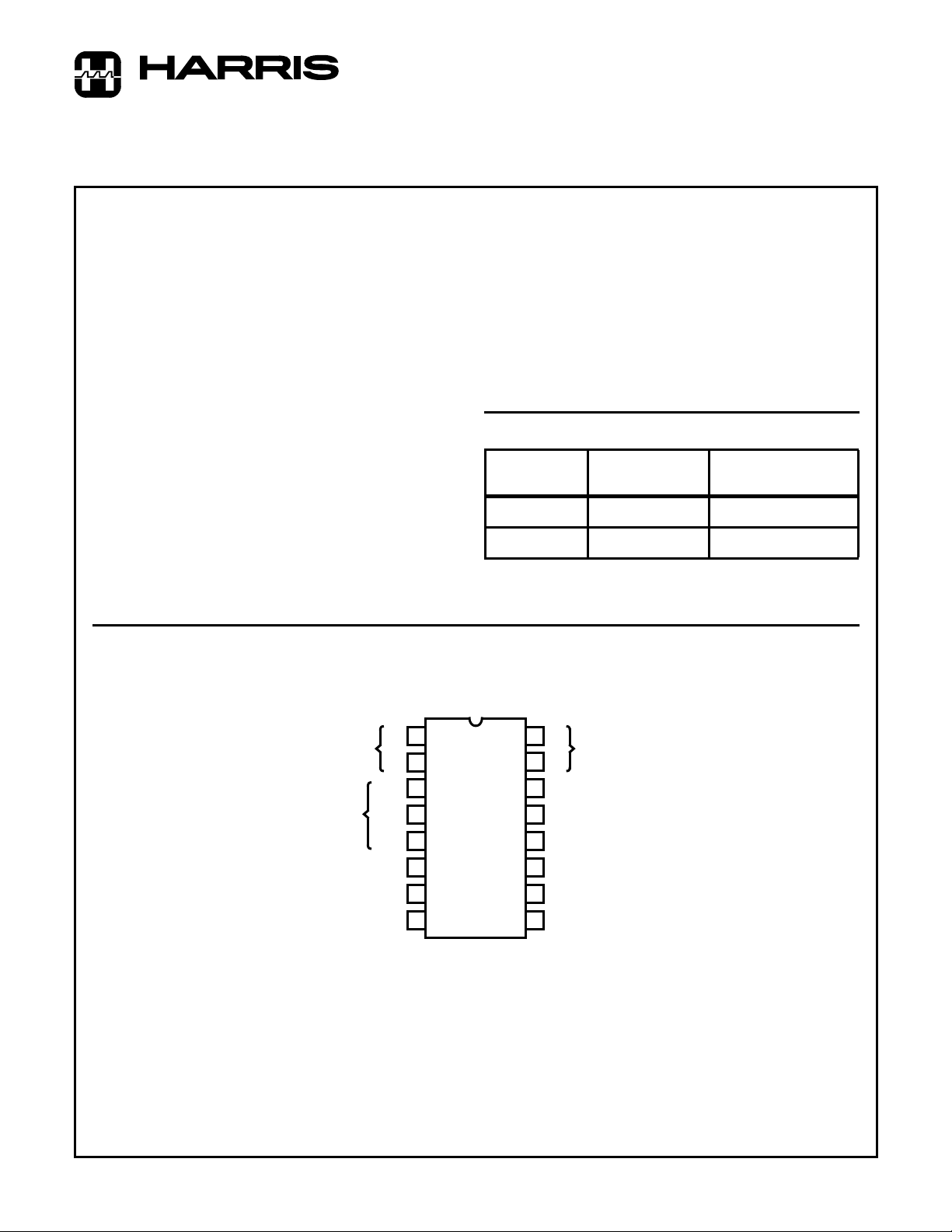
Ordering Information
PART
NUMBER
CA3162E 0oC to +70oC 16 Lead Plastic DIP
CA3162AE -40oC to +85oC 16 Lead Plastic DIP
TEMPERATURE
RANGE PACKAGE
Pinout
BCD
OUTPUTS
DIGIT
SELECT
OUTPUTS
ZERO ADJ
NSD
MSD
LSD
HOLD/
BYPASS
GND
1
1
2
0
2
2
3
4
5
6
7
8
CA3162 (PDIP)
TOP VIEW
3
16
2
2
15
2
14
V+
13
GAIN ADJ
INTEGRATING
12
CAP
11
HIGH INPUT
10
LOW INPUT
9
ZERO ADJ
BCD
OUTPUTS
CAUTION: These devices are sensitive to electrostatic discharge. Users should follow proper I.C. Handling Procedures.
Copyright
© Harris Corporation 1993
2-5
File Number
1080.1
Page 2
Functional Block Diagram
ZERO
ADJ
8 9 12 1 2 15 16 14
HIGH INPUT
LOW INPUT
11
10
V/I
CONVERTER
CA3162, CA3162A
V+V+
INTEGRATING
CAP
CONTROL LOGIC
COUNTERS & MULTIPLEX
THRESHOLD
DET.
BCD OUTPUTS
2120222
÷2048
3
DIGIT
DRIVE
V+
3
4
5
DIGIT SELECT
OUTPUTS †
4
= MSD
5
= LSD
3
= NSD
÷96
†
MSD = MOST SIGNIFICANT DIGIT
NSD = NEXT SIGNIFICANT DIGIT
LSD = LEAST SIGNIFICANT DIGIT
REFERENCE
CURRENT
GENERATOR
BAND GAP
REFERENCE
GAIN
ADJ
OSC
HOLD/
BYPASS
GATES
CONVERSION
6
CONTROL
713
GND
2-6
Page 3
Specifications CA3162, CA3162A
Absolute Maximum Ratings Thermal Information
DC Supply Voltage (Between Pins 7 & 14). . . . . . . . . . . . . . . . . +7V
Input Voltage (Pin 10 or 11 to Ground). . . . . . . . . . . . . . . . . . . . . ±15V
Storage Temperature Range . . . . . . . . . . . . . . . . . -65oC to +150oC
Lead Temperature (Soldering 10s). . . . . . . . . . . . . . . . . . . . +300oC
CAUTION: Stresses above those listed in “Absolute Maximum Ratings” may cause permanent damage to the device. This is a stress only rating and operation
of the device at these or any other conditions above those indicated in the operational sections of this specification is not implied.
Thermal Resistance θ
JA
Plastic DIP Package . . . . . . . . . . . . . . . . . . . . . . . . . . 90oC/W
Operating Temperature Range
CA3162E. . . . . . . . . . . . . . . . . . . . . . . . . . . . . . . . . . . .0 to +75oC
CA3162AE. . . . . . . . . . . . . . . . . . . . . . . . . . . . . . .-40oC to +85oC
Maximum Power Dissipation
Plastic DIP Package . . . . . . . . . . . . . . . . . . . . . . . . . . . . . . 0.67W
Junction Temperature . . . . . . . . . . . . . . . . . . . . . . . . . . . . . . +150oC
Electrical Specifications T
= +25oC, V+ = 5V, Zero Pot Centered, Gain Pot = 2.4kΩ Unless Otherwise Specified
A
PARAMETERS TEST CONDITIONS MIN TYP MAX UNITS
Operating Supply Voltage Range, V+ 4.5 5 5.5 V
Supply Current, I+ 100kΩ to V+ on Pins 3, 4, 5 - - 17 mA
Input Impedance, Z
Input Bias Current, I
I
IB
Pins 10 and 11 - -80 - nA
- 100 - MΩ
Unadjusted Zero Offset V11-V10 = 0V, Read Decoded Output -12 - +12 mV
Unadjusted Gain V11-V10 = 900mV, Read Decoded Output 846 - 954 mV
Linearity Notes 1 and 2 -1 - +1 Count
Conversion Rate
Slow Mode Pin 6 = Open or GND - 4 - Hz
Fast Mode Pin 6 = 5V - 96 - Hz
Conversion Control Voltage (Hold Mode)
0.8 1.2 1.6 V
at Pin 6
Common Mode Input Voltage Range, V
ICR
Notes 3, 4 -0.2 - +0.2 V
BCD Sink Current at Pins 1, 2, 15, 16 V
Digit Select Sink Current at Pins 3, 4, 5 V
≥ 0.5V, at Logic Zero State 0.4 1.6 - mA
BCD
Select = 4V at Logic Zero State 1.6 2.5 - mA
DIGIT
Zero Temperature Coefficient VI = 0V, Zero Pot Centered - 10 - µV/oV
Gain Temperature Coefficient VI = 900mV, Gain Pot = 2.4kΩ - 0.005 - %/oC
NOTES:
1. Apply zero volts across V11 to V10. Adjust zero potentiometer to give 000mV reading. Apply 900mV to input and adjust gain potentiometer
to give 900mV reading.
2. Linearity is measured as a difference from a straight line drawn through zero and positive full scale. Limits do not include ±0.5 count bit
digitizing error.
3. For applications where low input pin 10 is not operated at pin 7 potential, a return path of not more than 100kΩ resistance must be provided
for input bias currents.
4. The common mode input voltage above ground cannot exceed +0.2V if the full input signal range of 999mV is required at pin 11. That is,
pin 11 may not operate higher than 1.2V positive with respect to ground or 0.2V negative with respect to ground. If the maximum input
signal is less than 999mV, the common mode input voltage may be raised accordingly.
2-7
Page 4

CA3162, CA3162A
Timing Diagram
12
5 (LSD)
4 (MSD)
PIN NUMBER
3 (NSD)
2ms/DIVISION
FIGURE 1. HIGH SPEED MODE
200mV
500mV
500mV
500mV
Detailed Description
The Functional Block Diagram of the CA3162E shows the V/I
converter and reference current generator, which is the heart
of the system. The V/I converter converts the input voltage
applied between pins 10 and 11 to a current that charges the
integrating capacitor on pin 12 for a predetermined time interval. At the end of the charging interval, the V/I converter is disconnected from the integrating capacitor, and a band gap
reference constant current source of opposite polarity is connected. The number of clock counts that elapse before the
charge is restored to its original value is a direct measure of
the signal induced current. The restoration is sensed by the
comparator, which in turn latches the counter. The count is
then multiplexed to the BCD outputs.
The timing for the CA3162E is supplied by a 786Hz ring oscillator, and the input at pin 6 determines the sampling rate. A
5V input provides a high speed sampling rate (96Hz), and
grounding or floating pin 6 provides a low speed (4Hz) sampling rate. When pin 6 is fixed at +1.2V (by placing a 12K
resistor between pin 6 and the +5V supply) a “hold” feature is
available. While the CA3162E is in the hold mode, sampling
continues at 4Hz but the display data are latched to the last
reading prior to the application of the 1.2V. Removal of the
1.2V restores continuous display changes. Note, however,
that the sampling rate remains at 4Hz.
Figure 1 shows the timing of sampling and digit select pulses
for the high speed mode. Note that the basic A/D conversion
process requires approximately 5ms in both modes.
The “EEE” or “---” displays indicate that the range of the system has been exceeded in the positive or negative direction,
respectively. Negative voltages to -99mV are displayed with
the minus sign in the MSD. The BCD code is 1010 for a negative overrange (---) and 101 1 for a positive overrange (EEE).
NORMAL
LOW SPEED MODE:
V6 = GROUND OR
OPEN
HOLD:
= 1.2V
V
6
HIGH SPEED MODE:
= 5V
V
6
11
HIGH
INPUTS
LOW
10
0.27µF
16 1616 16
6
CA3162E
GAIN
ADJ
NOTE 1
10
kΩ
713
NOTE 2
0.1
µF
5
3
4
DIGIT
DRIVERS
BCD
OUTPUTS
6
16
2
15
1
1
7
2
+5V
16
CA3161E
COMMON
ANODE LED
a
f
g
e
d
CA3162E
PINS
DISPLAYS
b
c
R2
150Ω
MSD NSD LSD
a
f
b
g
e
c
d
13
12
11
10
9
15
14
38
CA3162E
PINS
3, 4, 5
R1
150Ω
1, 2, 15, 16
POWER
2N2907, 2N3906
OR EQUIV.
a
f
b
g
e
c
d
R3
150Ω
NOTES:
1. The capacitor used here must be a low dielectric absorption type
such as a polyester or polystyrene type.
2. This capacitor should be placed as close as possible to the power
and ground Pins of the CA3161E.
FIGURE 2. BASIC DIGITAL READOUT SYSTEM USING THE CA3162E AND THE CA3161E
2-8
1kΩ
DIGIT
DRIVER
75Ω
BCD SEGMENT
DRIVERS
Page 5

CA3162, CA3162A
CA3162E Liquid Crystal Display (LCD) Application
Figure 3 shows the CA3162E in a typical LCD application.
LCDs may be used in favor of LED displays in applications
requiring lower power dissipation, such as battery-operated
equipment, or when visibility in high-ambient-light conditions
is desired.
Multiplexing of LCD digits is not practical, since LCDs must
be driven by an AC signal and the average voltage across
each segment is zero. Three CD4056B liquid-crystal
decoder/drivers are therefore used. Each CD4056B contains
an input latch so that the BCD data for each digit may be
latched into the decoder using the inverted digit-select outputs of the CA3162E as strobes.
The capacitors on the outputs of inverters G3 and G4 filter
out the decode spikes on the MSD and NSD signals. The
capacitors and pull-up resistors connected to the MSD, NSD
0.047µF
+5V
6 x
10kΩ
0.27µF
MSD
1214
4
NSD
3
LSD
5
3
2
16
2
2
15
1
2
1
0
2
2
4 x
7
100kΩ
+5V
HEX INVERTER
TRIPLE 3 INPUT NAND GATE
0.047µF
0.047
µF
G8
G7
50kΩ
“HOLD”
V
IN
VIN-
ZERO
8
9
CA3162E
+
11
10
GAIN
10kΩ
G1 - G6: CD4049UB
G7, G8, G9: CD4023B
13
and LSD outputs are there to shorten the digit drive signal
thereby providing proper timing for the CD4056B latches.
Inverters G1 and G2 are used as an astable multivibrator to
provide the AC drive to the LCD backplane. Inverters G3, G4
and G5 are the digit-select inverters and require pull-up
resistors to interface the open-collector outputs of the
CA3162E to CMOS logic. The BCD outputs of the CA3162E
may be connected directly to the corresponding CD4056B
inputs (using pull-up resistors). In this arrangement, the
CD4056B decodes the negative sign (-) as an “L” and the
positive overload indicator (E) as an “H”.
The circuit as shown in Figure 3 using G7, G8 and G9 will
decode the negative sign (-) as a negative sign (-), and the
positive overload indicator (E) as “H”.
+5V
16
CD4056B
78
+5V
16
CD4056B
78
+5V
16
CD4056B
78
TO MSD
OF LCD
TO NSD
OF LCD
TO LSD
OF LCD
TO LCD
BACKPLANE
G4
G3
G5
0.047
G9
µF
0.047µF
1
6
4
2
3
5
1
6
4
2
3
5
1
6
4
2
3
5
FIGURE 3. TYPICAL LCD APPLICATION
2-9
15kΩ
100kΩ 0.63µF
Page 6

CA3162, CA3162A
CA3162E Common-Cathode, LED Display Application
Figure 4 shows the CA3162E connected to a CD4511B
decode/driver to operate a common-cathode LED display.
Unlike the CA3161E, the CD4511B remains blank for all
BCD codes greater than nine. After 999mV the display
blanks rather than displaying EEE, as with the CA3161E.
When displaying negative voltage, the first digit remains
blank, instead of (-), and during a negative or positive overrange the display blanks.
V+
100kΩDP1
1/6 CD4049UB
1/6 CD4049UB
DP2
CD4012B
The additional logic shown within the dotted area of Figure 4
restores the negative sign (-), allowing the display of negative numbers as low as -99mV. Negative overrange is indicated by a negative sign (-) in the MSD position. The rest of
the display is blanked. During a positive overrange, only segment b of the MSD is displayed. One inverter from the
CD4049B is used to operate the decimal points. By connecting the inverter input to either the MSD or NSD line either
DP1 or DP2 will be displayed.
22kΩ
1/3
CD4049UB
1/3
CD4049UB
100kΩ100
kΩ
V+
100
kΩ
100kΩ100kΩ
V+
100kΩ 100kΩ
B
1
CA3162E
A
2
3
4
5
6
7
8
NSD
MSD
LSD
HOLD
GND
ZERO
V+
GAIN
INT
HIGH
LOW
ZERO
V+
50kΩ
1
B
CD4511B
C
2
3
LT
4
BL
LE/
5
STROBE
D
6
A
7
GND
8
16
D
C
15
0.27µF
INPUT
V+
10kΩ
GAIN
14
13
12
11
10
9
V+
f
g
a
b
c
d
e
1.8kΩ
15
14
1.8kΩ
13
12
1.8kΩ
11
1.8kΩ
10
1.8kΩ
9
1.2kΩ
1.2kΩ
12 11 10 9 8 7
c1edc2cd
HP5082-7433
OR EQUIVALENT
fagbc
DP1 DP2
3
P
654321
6 BUFFERS
(1 CD4050B)
V+
16
FIGURE 4. TYPICAL COMMON-CATHODE LED APPLICATION
2-10
Page 7

Die Characteristics
DIE DIMENSIONS:
101 x 124 x 20 ± 1mils
METALLIZATION:
Type: Al
Thickness: 17.5k
Å ± 2.5kÅ
GLASSIVATION:
Type: 3% PSG
Thickness: 13k
Å ± 2.5kÅ
Metallization Mask Layout
CA3162, CA3162A
CA3162, CA3162A
HIGH INPUT
INTEGRATING CAP
GAIN ADJ
LOW INPUT
ZERO ADJ
ZERO ADJ
GND
HOLD/BYPASS
LSD
MSD
V+
1
2
2
3
2
0
2
2
NSD
2-11
 Loading...