

Datasheet CA3080M96, CA3080M, CA3080E, CA3080AM96, CA3080AM Datasheet (Harris Semiconductor)
...Page 1
SEMICONDUCTOR
November 1996
CA3080, CA3080A
2MHz, Operational
Transconductance Amplifier (OTA)
Features
• Slew Rate (Unity Gain, Compensated). . . . . . . . 50V/µs
• Adjustable Power Consumption . . . . . . . . . 10 µW to 30µW
• Flexible Supply Volta ge Range . . . . . . . . . . ±2V to ±15V
• Fully Adjustable Gain . . . . . . . . . . . . . .0 to g
• Tight g
Spread:
M
MRL
Limit
- CA3080 . . . . . . . . . . . . . . . . . . . . . . . . . . . . . . . . . . 2:1
- CA3080A . . . . . . . . . . . . . . . . . . . . . . . . . . . . . . . . 1.6:1
• Extended g
Linearity. . . . . . . . . . . . . . . . . . 3 Decades
M
Applications
• Sample and Hold • Multiplier
• Multiplexer • Comparator
• Voltage Follower
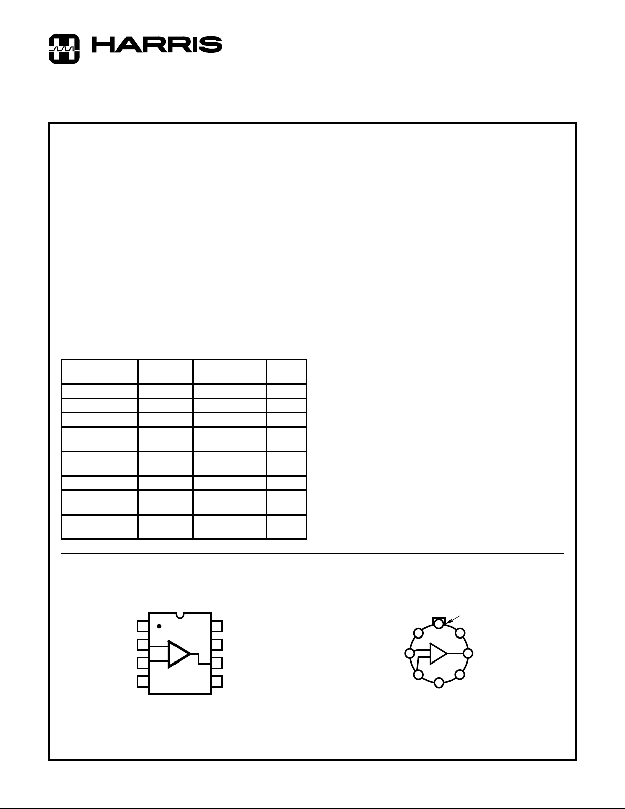
Ordering Information
PART NUMBER
(BRAND)
CA3080 0 to 70 8 Pin Metal Can T8.C
CA3080A -55 to 125 8 Pin Metal Can T8.C
CA3080AE -55 to 125 8 Ld PDIP E8.3
CA3080AM
(3080A)
CA3080AM96
(3080A)
CA3080E 0 to 70 8 Ld PDIP E8.3
CA3080M
(3080)
CA3080M96
(3080)
TEMP.
RANGE (oC) PACKAGE
-55 to 125 8 Ld SOIC M8.15
-55 to 125 8 Ld SOIC Tape
and Reel
0 to 70 8 Ld SOIC M8.15
0 to 70 8 Ld SOIC T ape
and Reel
M8.15
M8.15
PKG.
NO.
Description
The CA3080 and CA3080A types are Gatable-Gain Blocks
which utilize the unique operational-transconductanceamplifier (OTA) concept described in Application Note
AN6668, “Applications of the CA3080 and CA3080A HighPerformance Operational Transconductance Amplifiers”.
The CA3080 and CA3080A types have differential input and a
single-ended, push-pull, class A output. In addition, these types
have an amplifier bias input which ma y be used either f or gating
or for linear gain control. These types also have a high output
impedance and their transconductance (g
proportional to the amplifier bias current (I
The CA3080 and CA3080A types are notable for their e xcellent
slew rate (50V/µs), which makes them especially useful for
multiplexer and fast unity-gain voltage followers. These types
are especially applicable for multiplexer applications because
power is consumed only when the devices are in the “ON”
channel state.
The CA3080A’s characteristics are specifically controlled for
applications such as sample-hold, gain-control, multiplexing, etc.
ABC
) is directly
M
).
Pinouts
CA3080
(PDIP, SOIC)
TOP VIEW
1
NC
INV.
INPUT
NON-INV.
INPUT
NOTE: Pin 4 is connected to case.
CAUTION: These devices are sensitive to electrostatic discharge. Users should follow proper IC Handling Procedures.
Copyright
© Harris Corporation 1996
2
-
+
3
4
V-
8
NC
7
V+
6
OUTPUT
AMPLIFIER
5
BIAS INPUT
3-45
INV.
INPUT
NON-INV.
INPUT
2
CA3080
(METAL CAN)
TOP VIEW
8
1
3
7
-
+
5
4
V-
TAB
V+
OUTPUT
6
BIAS
File Number 475.3
Page 2
CA3080, CA3080A
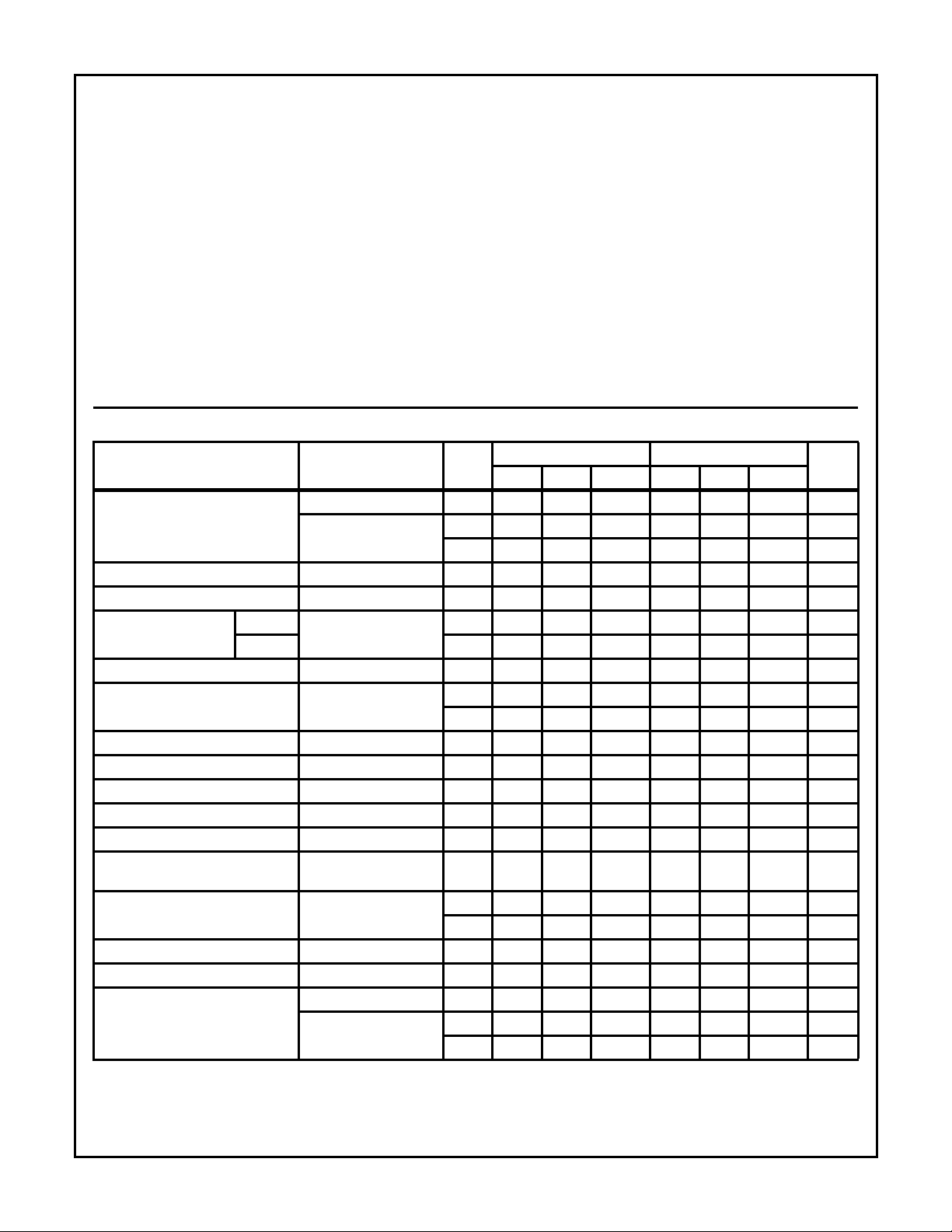
Absolute Maximum Ratings Thermal Information
Supply Voltage (Between V+ and V- Terminal). . . . . . . . . . . . . . 36V
Differential Input Voltage. . . . . . . . . . . . . . . . . . . . . . . . . . . . . . . . 5V
Input Voltage. . . . . . . . . . . . . . . . . . . . . . . . . . . . . . . . . . . . . V+ to V-
Input Signal Current . . . . . . . . . . . . . . . . . . . . . . . . . . . . . . . . . 1mA
Amplifier Bias Current (I
) . . . . . . . . . . . . . . . . . . . . . . . . . . 2mA
ABC
Output Short Circuit Duration (Note 1) . . . . . . . . . . . . No Limitation
Operating Conditions
Temperature Range
CA3080. . . . . . . . . . . . . . . . . . . . . . . . . . . . . . . . . . . . 0oC to 70oC
CA3080A . . . . . . . . . . . . . . . . . . . . . . . . . . . . . . . -55oC to 125oC
CAUTION: Stresses above those listed in “Absolute Maximum Ratings” may cause permanent damage to the device. This is a stress only rating and operation
of the device at these or any other conditions above those indicated in the operational sections of this specification is not implied.
NOTES:
1. Short circuit may be applied to ground or to either supply.
2. θJA is measured with the component mounted on an evaluation PC board in free air.
Thermal Resistance (Typical, Note 2) θJA (oC/W) θJC (oC/W)
PDIP Package. . . . . . . . . . . . . . . . . . . 130 N/A
SOIC Package. . . . . . . . . . . . . . . . . . . 170 N/A
Metal Can Package. . . . . . . . . . . . . . . 200 120
Maximum Junction Temperature (Metal Can) . . . . . . . . . . . . . 175oC
Maximum Junction Temperature (Plastic Package) . . . . . . . 150oC
Maximum Storage Temperature Range . . . . . . . . . -65oC to 150oC
Maximum Lead Temperature (Soldering 10s). . . . . . . . . . . . 300oC
(SOIC - Lead Tips Only)
Electrical Specifications For Equipment Design, V
PARAMETER TEST CONDITIONS TEMP
Input Offset Voltage I
Input Offset Voltage Change I
Input Offset Voltage Temp. Drift I
Input Offset Voltage
Sensitivity
Positive I
Negative 25 - - 150 - - 150 µV/V
Input Offset Current I
Input Bias Current I
Differential Input Current I
Amplifier Bias Voltage I
Input Resistance I
Input Capacitance I
Input-to-Output Capacitance I
Common-Mode Input-Voltage
Range
Forward Transconductance
(Large Signal)
Output Capacitance I
Output Resistance I
Peak Output Current I
= 5µA 25 - 0.3 - - 0.3 2 mV
ABC
= 500µA 25 - 0.4 5 - 0.4 2 mV
I
ABC
= 500µA to 5µA 25 - 0.2 - - 0.1 3 mV
ABC
= 100µA Full - - - - 3.0 - µV/oC
ABC
= 500µA 25 - - 150 - - 150 µV/V
ABC
= 500µA 25 - 0.12 0.6 - 0.12 0.6 µΑ
ABC
= 500µA25-25-25µA
ABC
= 0, V
ABC
= 500µA 25 - 0.71 - - 0.71 - V
ABC
= 500µA 251026-1026-kΩ
ABC
= 500µA, f = 1MHz 25 - 3.6 - - 3.6 - pF
ABC
= 500µA, f = 1MHz 25 - 0.024 - - 0.024 - pF
ABC
= 500µA 25 12 to
I
ABC
= 500µA 25 6700 9600 13000 7700 9600 12000 µS
I
ABC
= 500µA, f = 1MHz 25 - 5.6 - - 5.6 - pF
ABC
= 500µA 25 - 15 - - 15 - MΩ
ABC
= 5µA, RL = 0Ω 25 - 5 - 3 5 7 µA
ABC
= 500µA, RL = 0Ω 25 350 500 650 350 500 650 µA
I
ABC
= 4V 25 - 0.008 - - 0.008 5 nA
DIFF
= ±15V, Unless Otherwise Specified
SUPPLY
CA3080 CA3080A
Full - - 6 - - 5 mV
Full - - 7 - - 15 µA
-12
13.6 to
-14.6
- 12 to
-12
13.6 to
-14.6
Full 5400 - - 4000 - - µS
Full 300 - - 300 - - µA
UNITSMIN TYP MAX MIN TYP MAX
-V
3-46
Page 3
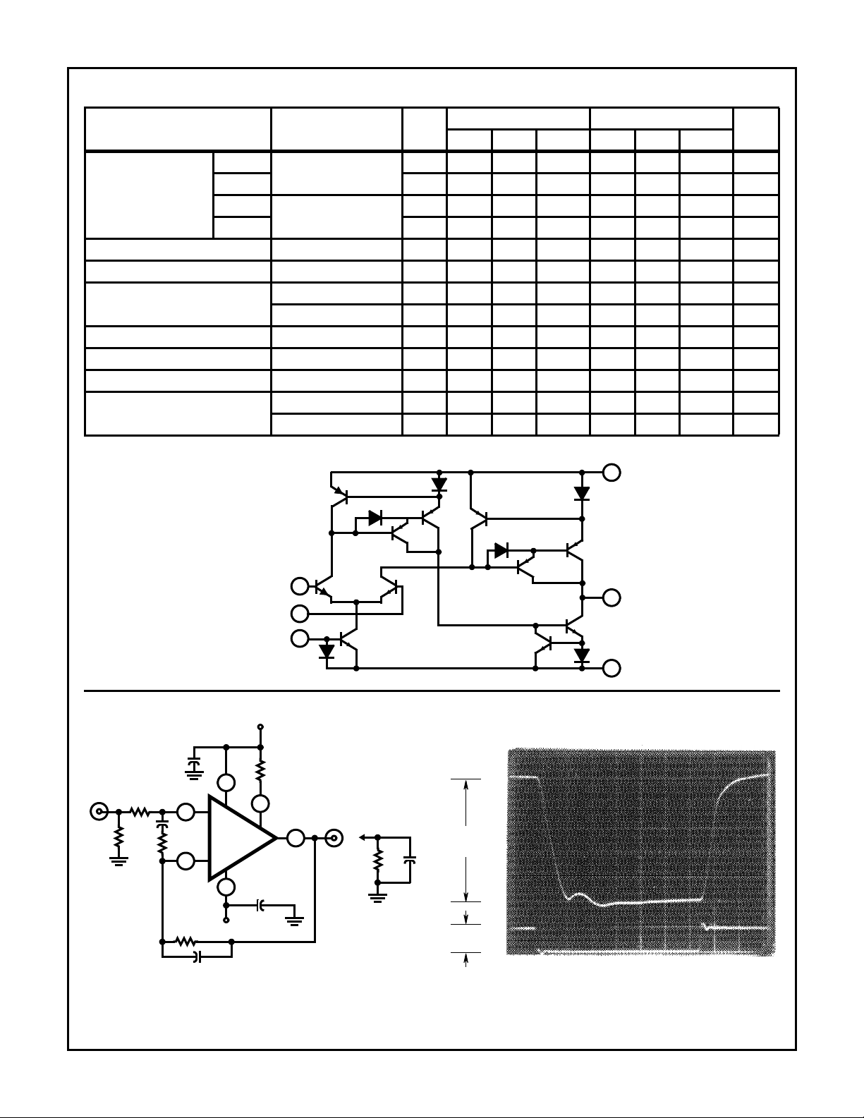
CA3080, CA3080A
Electrical Specifications For Equipment Design, V
= ±15V, Unless Otherwise Specified (Continued)
SUPPLY
CA3080 CA3080A
Peak Output
Voltage
PARAMETER TEST CONDITIONS TEMP
Positive I
= 5µA, RL = ∞ 25 - 13.8 - 12 13.8 - V
ABC
Negative 25 - -14.5 - -12 -14.5 - V
Positive I
= 500µA, RL = ∞ 25 12 13.5 - 12 13.5 - V
ABC
UNITSMIN TYP MAX MIN TYP MAX
Negative 25 -12 -14.4 - -12 -14.4 - V
Amplifier Supply Current I
Device Dissipation I
Magnitude of Leakage Current
Propagation Delay I
Common-Mode Rejection Ratio I
Open-Loop Bandwidth I
= 500µA 25 0.8 1 1.2 0.8 1 1.2 mA
ABC
= 500µA 252430 36 2430 36mW
ABC
I
= 0, VTP = 0 25 - 0.08 - - 0.08 5 nA
ABC
= 0, VTP = 36V 25 - 0.3 - - 0.3 5 nA
I
ABC
= 500µA 25 - 45 - - 45 - ns
ABC
= 500µA 25 80 110 - 80 110 - dB
ABC
= 500µA 25 - 2 - - 2 - MHz
ABC
Slew Rate Uncompensated 25 - 75 - - 75 - V/µs
Compensated 25 - 50 - - 50 - V/µs
Schematic Diagram
+
7
V
9
OUTPUT
6
10
V-
4
INVERTING
INPUT
NONINVERTING
INPUT
AMPLIFIER
BIAS INPUT
D
Q6Q
3
7
D
4
Q
4
D
2
Q
5
2
Q
Q
1
2
3
5
Q
3
D
1
D
3
Q
Q
8
Q
Q
11
D
6
Typical Applications
V+ = 15V
51Ω
10kΩ
300Ω
0.01µF
3
390pF
2
10kΩ
0.001µF
7
+
CA3080, A
-
4
V- = -15V
5
0.01µF
62kΩ
LOAD
(SCOPE PROBE)
6
1MΩ
5pF
OUTPUT
1V/DIV.
INPUT
5V/DIV.
FIGURE 1. SCHEMATIC DIAGRAM OF THE CA3080 AND CA3080A IN A UNITY-GAIN VOLTAGE FOLLOWER CONFIGURATION
AND ASSOCIATED WAVEFORM
3-47
VS = ±15V
TIME -0.1µs/DIV.
Page 4

CA3080, CA3080A
Typical Applications
50mV
0
-50mV
(Continued)
IN
51Ω
INPUT
OUTPUT
FIGURE 13. PROPAGATION DELAY TEST CIRCUIT AND ASSOCIATED WAVEFORMS
Typical Performance Curves
5
SUPPLY VOLTS: VS = ±15V
4
3
2
-55oC
1
0
-1
-2
-3
-4
-5
-6
INPUT OFFSET VOLTAGE (mV)
-7
-8
0.1 1 10 100 1000
70oC
90oC
25oC
125oC
AMPLIFIER BIAS CURRENT (µA)
90oC
-55oC
3
2
t
PLH
125oC
25oC
70oC
V+ = 15V
7
+
CA3080,A
-
4
V- = -15V
56kΩ
= 500µA
I
ABC
5
6
1N914
t
PHL
3
10
SUPPLY VOLTS: VS = ±15V
2
10
10
1
0.1
INPUT OFFSET CURRENT (nA)
0.01
0.1 1 10 100 1000
OUT
1.2MΩ
-55oC
25oC
125oC
AMPLIFIER BIAS CURRENT (µA)
0
FIGURE 14. INPUT OFFSET VOLTAGE vs AMPLIFIER BIAS
CURRENT
4
10
SUPPLY VOLTS: VS = ±15V
3
10
2
10
10
1
INPUT BIAS CURRENT (nA)
0.1
0.1 1 10 100 1000
AMPLIFIER BIAS CURRENT (µA)
125oC
-55oC
25oC
FIGURE 16. INPUT BIAS CURRENT vs AMPLIFIER BIAS CURRENT
FIGURE 15. INPUT OFFSET CURRENT vs AMPLIFIER BIAS
CURRENT
4
10
SUPPLY VOLTS: VS = ±15V
LOAD RESISTANCE = 0Ω
3
10
2
10
10
1
PEAK OUTPUT CURRENT (µA)
0.1
0.1 1 10 100 1000
AMPLIFIER BIAS CURRENT (µA)
25oC
FIGURE 17. PEAK OUTPUT CURRENT vs AMPLIFIER BIAS
CURRENT
3-52
125oC
-55oC
Page 5

CA3080, CA3080A
Typical Performance Curves
15
SUPPLY VOLTS: VS = ±15V
= 25oC
T
A
14.5
LOAD RESISTANCE =
14
13.5
13
0
-13
-13.5
-14
PEAK OUTPUT VOLTAGE (V)
-14.5
COMMON MODE INPUT VOLTAGE (V)
-15
0.1 1 10 100 1000
AMPLIFIER BIAS CURRENT (µA)
∞
(Continued)
V-
V-
CMR
V+
V+
OM
FIGURE 18. PEAK OUTPUT VOLTAGE vs AMPLIFIER BIAS
CURRENT
5
10
TA = 25oC
4
10
3
10
2
10
10
DEVICE POWER DISSIPATION (µW)
1
0.1 1 10 100 1000
VS = ±15V
VS = ±6V
VS = ±3V
AMPLIFIER BIAS CURRENT (µA)
CMR
OM
4
10
SUPPLY VOLTS: VS = ±15V
3
10
2
10
10
125oC
1
AMPLIFIER SUPPLY CURRENT (µA)
0.1
0.1 1 10 100 1000
-55oC, 25oC
AMPLIFIER BIAS CURRENT (µA)
125oC
25oC
-55oC
FIGURE 19. AMPLIFIER SUPPLY CURRENT vs AMPLIFIER
BIAS CURRENT
5
10
SUPPLY VOLTS: VS = ±15V
4
10
3
10
2
10
10
FORWARD TRANSCONDUCTANCE (µS)
1
0.1 1 10 100 1000
125oC
25oC
AMPLIFIER BIAS CURRENT (µA)
-55oC
FIGURE 20. TO TAL POWER DISSIP ATION vs AMPLIFIER BIAS
CURRENT
+36V
36V
0V
1
TEST POINT
(V
)
TP
2
CA3080, A
3
7
6
5
4
FIGURE 21. TRANSCONDUCT ANCE vs AMPLIFIER BIAS
CURRENT
100
SUPPLY VOLTS: VS = ±15V
10
V2 = V3 = V6 = 36V
1
0V
0.1
MAGNITUDE OF LEAKAGE CURRENT (nA)
0.01
-25 50 100
-50 0 25 75 125
TEMPERATURE (
o
C)
FIGURE 22. LEAKAGE CURRENT TEST CIRCUIT FIGURE 23. LEAKAGE CURRENT vs TEMPERATURE
3-53
Page 6

CA3080, CA3080A
Typical Performance Curves
2
1
V
= ±4V
DIFF
3
(Continued)
V+ = 15V
CA3080, A
4
V- = -15V
SUPPLY VOLTS: VS = ±15V
4
10
3
7
6
5
10
125oC
2
10
10
1
DIFFERENTIAL INPUT CURRENT (pA)
01234 567
INPUT DIFFERENTIAL VOLTAGE (V)
25oC
FIGURE 24. DIFFERENTIAL INPUT CURRENT TEST CIRCUIT FIGURE 25. INPUT CURRENT vs INPUT DIFFERENTIAL VOLTAGE
SUPPLY VOLTS: VS = ±15V
= 25oC
T
A
100
10
1
0.1
INPUT RESISTANCE (MΩ)
0.01
0.1 1 10 100 1000
AMPLIFIER BIAS CURRENT (µA)
SUPPLY VOLTS: VS = ±15V
900
800
700
600
500
400
300
200
100
AMPLIFIER BIAS VOLTAGE (mV)
0
0.1 1 10 100 1000
AMPLIFIER BIAS CURRENT (µA)
-55oC
25oC
125oC
FIGURE 26. INPUT RESISTANCE vs AMPLIFIER BIAS CURRENT
7
SUPPLY VOLTS: VS = ±15V
f = 1 MHz
6
T
= 25oC
A
5
C
4
3
2
1
INPUT AND OUTPUT CAPACITANCE (pF)
0
0.1 1 10 100 1000
AMPLIFIER BIAS CURRENT (µA)
O
C
I
FIGURE 28. INPUT AND OUTPUT CAP ACIT ANCE vs AMPLIFIER
BIAS CURRENT
FIGURE 27. AMPLIFIER BIAS VOLTAGE vs AMPLIFIER BIAS
CURRENT
5
10
4
10
3
10
2
10
10
OUTPUT RESISTANCE (MΩ)
1
0.1 1 10 100 1000
SUPPLY VOLTS: VS = ±15V
T
= 25oC
A
AMPLIFIER BIAS CURRENT (µA)
FIGURE 29. OUTPUT RESIST ANCE vs AMPLIFIER BIAS
CURRENT
3-54
Page 7

CA3080, CA3080A
Typical Performance Curves
2
CA3080, A
3
4
V-
V+
7
5
0.01µF
(Continued)
0.01µF
6
f = 1 MHz
T
= 25oC
A
0.06
0.05
0.04
0.03
0.02
0.01
INPUT - TO - OUTPUT CAPACITANCE (pF)
0 2 4 6 8 10121416 18
POSITIVE AND NEGATIVE SUPPLY VOLTAGE (V)
FIGURE 30. INPUT-TO-OUTPUT CAPACITANCE TEST CIRCUIT FIGURE 31. INPUT-TO-OUTPUT CAPACITANCE vs SUPPLY
VOLTAGE
All Harris Semiconductor products are manufactured, assembled and tested under ISO9000 quality systems certification.
Harris Semiconductor products are sold by description only. Harris Semiconductor reserves the right to make changes in circuit design and/or specifications at
any time without notice. Accordingly, the reader is cautioned to verify that data sheets are current before placing orders. Information furnished by Harris is
believed to be accurate and reliable. However, no responsibility is assumed by Harris or its subsidiaries for its use; nor for any infringements of patents or other
rights of third parties which may result from its use. No license is granted by implication or otherwise under any patent or patent rights of Harris or its subsidiaries.
Sales Office Headquarters
For general information regarding Harris Semiconductor and its products, call 1-800-4-HARRIS
NORTH AMERICA
Harris Semiconductor
P. O. Box 883, Mail Stop 53-210
Melbourne, FL 32902
TEL: 1-800-442-7747
(407) 729-4984
FAX: (407) 729-5321
EUROPE
Harris Semiconductor
Mercure Center
100, Rue de la Fusee
1130 Brussels, Belgium
TEL: (32) 2.724.2111
FAX: (32) 2.724.22.05
SEMICONDUCTOR
3-55
ASIA
Harris Semiconductor PTE Ltd.
No. 1 Tannery Road
Cencon 1, #09-01
Singapore 1334
TEL: (65) 748-4200
FAX: (65) 748-0400
 Loading...