

Page 1
Semiconductor
No. AN6157.1 April 1994
APPLICATIONS OF THE CA3085 SERIES MONOLITHIC
IC VOLTAGE REGULATORS
Authors: A.C.N. Sheng and L.R. Avery
The Harris CA3085, CA3085A, and CA3085B monolithic
IC’s are positive-voltage regulators capable of providing output currents up to 100mA over the temperature range from -
o
55
C to +125oC. They are supplied in 8 lead TO-5 type packages. The following tabulation shows some key characteristics and salient differences between devices in the CA3085
Series.
VIN (VI)
RANGE
TYPE
CA3085 7.5 - 30 1.8 - 26 12* 0.1
CA3085A 7.5 - 40 1.7 - 36 100 0.15
CA3085B 7.5 - 50 1.7 - 46 100 0.15
(V)
*This value may be extended to 100mA; however, regulation
is not specified beyond 12mA.
In addition to these differences, the range of some specified
performance parameters is more tightly controlled in the
CA3085B than in the CA3085A, and more in the CA3085A
than in the CA3085.
This note describes the basic circuit of the CA3085 series
devices and some typical applications that include a high
current regulator, constant current regulations, a switching
regulator, a negative-voltage regulator, a dual-tracking regulator, high-voltage regulators, and various methods of providing current limiting, A circuit in which the CA3085 is used as
a general-purpose amplifier is also shown.
Circuit Description
The block diagram of the CA3085 series circuits is shown in
Figure 1. Fundamentally, the circuit consists of a frequency
compensated error-amplifier which compares an internally
generated reference voltage with a sample of the output voltage and controls a series-pass amplifier to regulate the output. The starting circuit assures stable latch-in of the
voltage-reference circuitry. The current-limiting portion of the
circuit is an optional feature that protects the IC in the event
of overload.
Terminal 5 provides a source of stable reference voltage for
auxiliary use; a current of about 250µA can be supplied to an
external circuit without significantly disturbing reference-volt-
V
OUT
RANGE
(V)
(VO)
MAX.
I
OUT
(mA)
(IO)
MAX LOAD
REGULATION
( % VO)
Harris Intelligent Power
age stability. If necessary, filtering of the inherent noise of the
reference-voltage circuit can be accomplished by connecting
a suitable bypass capacitor between terminals 5 and 4.
Terminal 6 (the “inverting input” in accordance with operational-amplifier terminology) is the input through which a
sample of the regulated output voltage is applied.
COMPENSATION AND
UNREGULATED
VOLT.
STARTING
CIRCUIT
SUBSTRATE
REF.
AMPL.
SOURCE
V-
FIGURE 1. BLOCK DIAGRAM OF CA3085 SERIES
INPUT (V
CURRENT
SOURCE
V
REF
+
3
)
IN
+
FREQ.
COMP.
ERROR
AMPL.
-
INV
654 8
INPUT
The collector of the series-pass output transistor is brought
out separately at terminal 2 (“current booster”) to provide
base drive for an external p-n-p transistor; this approach is
one method of regulating currents greater than 100mA.
Because the voltage regulator is essentially an operational
amplifier having considerable feedback, frequency compensation is necessary in some circuits to prevent oscillations.
Terminal 7 is provided for if external frequency compensation is necessary. Terminal 7 can also be used to “inhibit”
(strobe, squelch, pulse, key) the operation of the series-pass
amplifier.
Brief Description of CA3085 Schematic Diagram
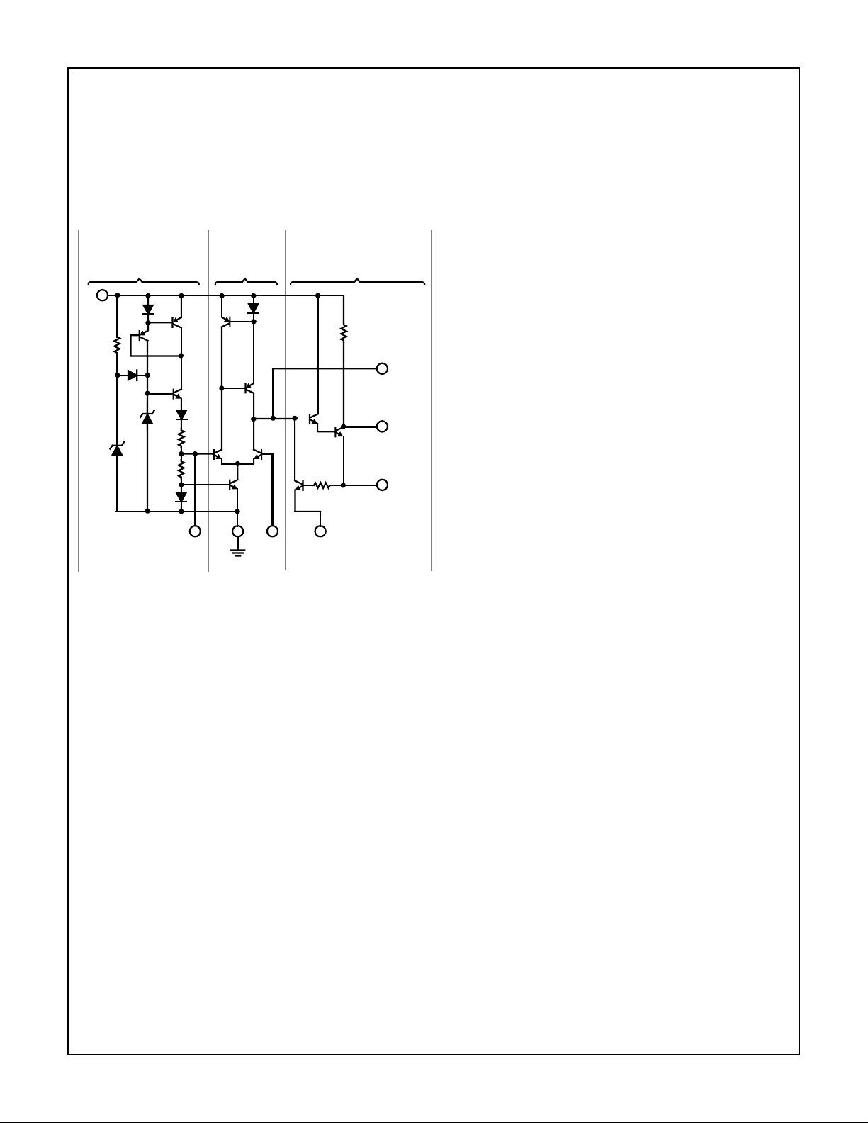
The schematic diagram of the CA3085 series circuits is
shown in Figure 2. The left-hand section includes the starting circuit, the voltage reference circuit, and the constantcurrent circuit. The center section is basically an elementary
operational amplifier which serves as the voltage-error
EXTERNAL INHIBIT
CURRENT
BOOSTER
SERIES
PASS
AMPL.
CURRENT
LIMITING
2 7
CURRENT
LIMITING
1
OUTPUT
REGULATED
Copyright © Harris Corporation 1992
11-52
Page 2
Application Note 6157
amplifier controlling the series-pass. Darlington pair (Q13,
Q14) shown in the right-hand section when controlled by an
appropriate external sensing network, transistor Q15, serves
to provide protective current-limiting characteristics by
diverting base drive from the series pass circuit. For operation at the highest current levels, terminals 2 and 3 are tied
together to eliminate the voltage drop which would otherwise
be developed across resistor R5.
VOLTAGE-REFERENCE,
STARTUP AND
CONSTANT-CURRENT
CIRCUITS
3
V+IN
UNREG.
INPUT
R
1
40k
D
1
ALL RESISTANCE VALUES
ARE IN Ω
D
6
Q
1
D
2
D
3
R
2
4k
R
3
1.5k
D
5
V
REF
FIGURE 2. SCHEMATIC DIAGRAM OF CA3085 SERIES
Q
2
Q
3
D
4
5
VOLTAGE-
ERROR
AMP (OP AMP)
Q
8
Q
Q
Q
6
5
Q
4
4
V-
INV.
INPUT
SUBSTRATE
SERIES-PASS AND CURRENT-
LIMITING CIRCUITS
D
7
R
5
500
R
1.5k
Q
13
4
8
COMPENSATION
AND EXTERNAL
INHIBIT
Q
14
REGULATED
9
6
Q15
CURRENT
LIMITING
7
2
CURRENT
BOOSTER
1
OUTPUT
Voltage Reference Circuits
The basic voltage referenced element used in the CA3085 is
zener diode D3. It provides a nominal reference voltage of
5.5V and exhibits a positive temperature coefficient of
approximately 2.5mV/
o
C. If this reference voltage were used
directly in conjunction with the error-amplifier (Q5, Q6, etc.),
the IC would exhibit two major undesirable characteristics:
(1) its performance with temperature variations would be
poor, and (2) its use as a regulator would be restricted to circuits in which the minimum regulated output voltages are in
excess of 5.5V. Consequently, it is necessary to provide
means of compensating for the positive temperature coefficient of D3 and at the same time provide for obtaining a stable source of lower reference voltage. Both temperature
compensation and the reduction of the reference voltage are
accomplished by means of the series divider network consisting of the base-emitter junction of Q3, diode D4, resistors
R2 and R3, and diode 5.
The voltage developed across D3 drives the divider network
and a voltage of approximately 4V is developed between the
cathode of D4 and the cathode of D5 (terminal 4). The current through this divider network is held nearly constant with
temperature because of the combined temperature coefficients of the zener diode (D3), Q3 base-emitter junction, D4,
D5, and the resistors R2 and R3. This constant current
through the diode D5 and the resistor R3 produces a voltage
drop between terminals 4 and 5 that results in the reference
voltage (≈ 1.6V) having an effective temperature coefficient
of about 0.0035%/
o
C.
The reference diode D3 receives a currant of approximately
620µA from a constant-current circuit consisting of Q3 and
the current-mirror* D6, Q1, and Q2. Current to start-up the
constant-current source initially is provided by auxiliary
zener diode D1 and R1. Diode D2 blocks current from the
R1-D1 source after latch-in of the constant-current source
establishes a stable reference potential, and thereby prevents modulation of the reference voltage by ripple voltage
on the unregulated input voltage.
Voltage-Error Amplifier
Transistors Q5 and Q6 comprise the basic differential amplifier that is used as a voltage-error amplifier to compare the
stable reference voltage applied at the base of Q5 with a
sample of the regulator output voltage applied at terminal 6.
The D5-Q4 combination is a current-mirror which maintains
essentially constant-current flow to Q5 and Q6 despite variations in the unregulated input voltage. The Q8, Q9, and D7
network provides a “mirrored” active collector load for Q5
and Q6 and also provides a variable single-ended drive to
the Q13 and Q14 series-pass transistors in accordance with
the difference signal developed between the bases of Q5
and Q6. The open-loop gain of the error-amplifier is greater
than 1000.
Series-Pass and Current-Limiting Circuits
In the normal mode of operation, or in the current-boost
mode when terminals 2 and 3 are tied together, the Darlington pair Q13-Q14 performs the basic series-pass regulating
function between the unregulated input voltage and the regulated output voltage at terminal 1. In the current-limiting
mode transistor Q15 provides current-limiting to protect the
CA3085 and/or limit the load current. To provide current-limiting protection, a resistor (e.g., 5Ω) is connected between
terminals 1 and 8; terminal 8 becomes the source of regulated output voltage. As the voltage drop across this resistor
increases, base drive is supplied to transistor Q15 so that it
becomes increasingly conductive and diverts base drive
from the Q13-Q14 pass transistor to reduce output current
accordingly. Resistor R4 is provided to protect Q15 against
overdrive by limiting its base current under transient and
load-short conditions.
Because the CA3085 regulator is essentially an op-amp
having considerable feedback, frequency compensation
may be required to prevent oscillations. Stability must also
be maintained despite line and load transients, even during
operation into reactive loads (e.g., filter capacitors). Provisions are included in the CA3085 so that a small-value
capacitor may be connected between terminals 6 and 7 to
compensate the regulator, when necessary, by “rolling-off”
the amplifier frequency-response. Terminal 7 is also used to
externally “inhibit” operation of the CA3085 by diverting base
current supplied to Q13-Q14, thereby permitting the use of
keying, strobing, programming, and/or auxiliary overloadprotection circuits.
11-53
Page 3
Application Note 6157
Applications
A Simple Voltage Regulator
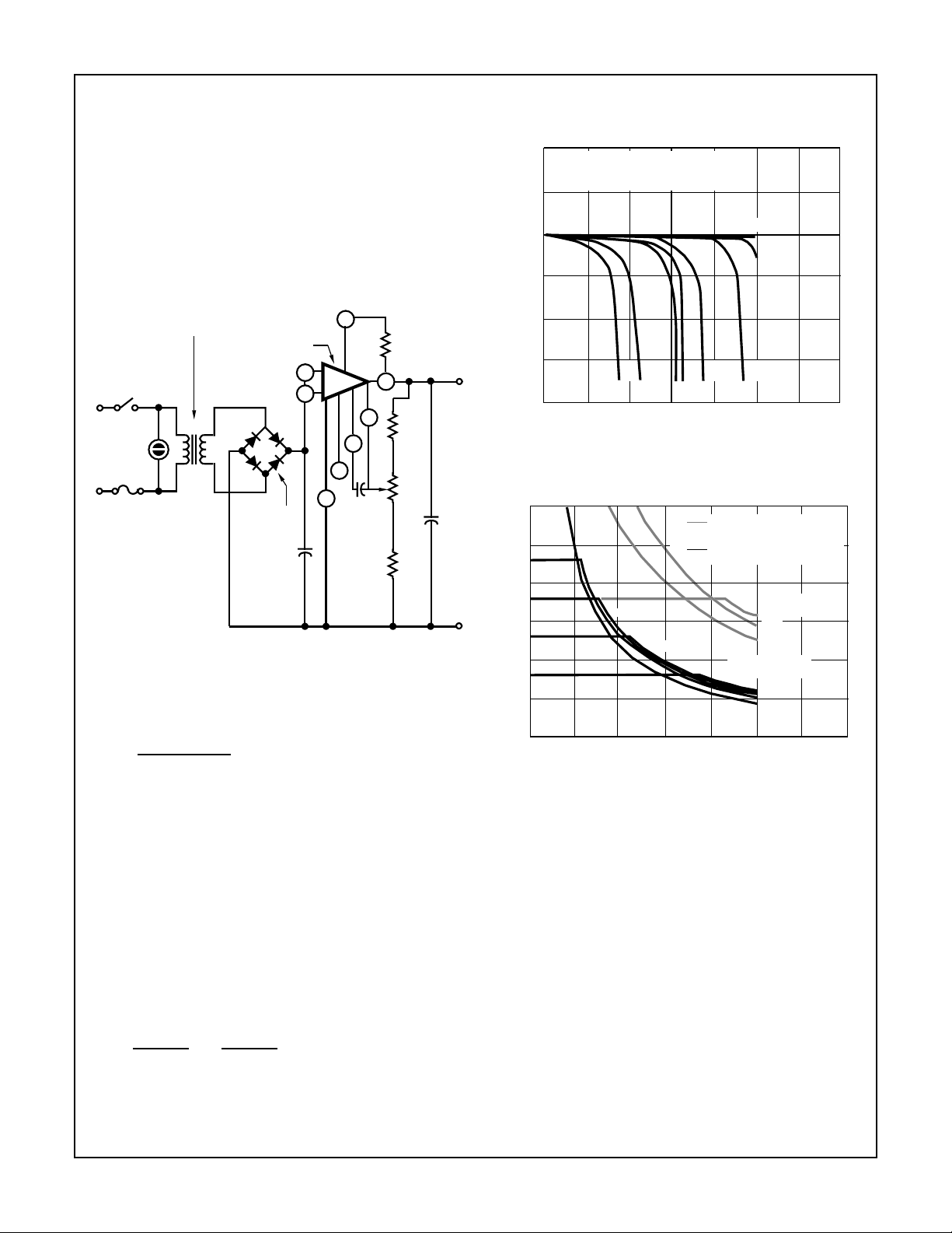
Figure 3 shows the schematic diagram of a simple regulated
power supply using the CA3085. The ac supply voltage is
stepped down by T1, full-wave rectified by the diode bridge
circuit, and smoothed by the large electrolytic capacitor C1
to provide unregulated dc to the CA3085 regulator circuit.
Frequency compensation of the error-amplifier is provided
by capacitor C2. Capacitor C3 bypasses residual noise in
the reference-voltage source, and thus decreases the incremental noise-voltage in the regulator circuit output.
TI: STANCOR TP3
CA3085, A, B
BLACK
WHITE
GREEN
120V
60Hz
BLACK
RED
(4)
1N3193
500µF
50V
+
-
FIGURE 3. BASIC POWER SUPPLY
Because the open-loop gain of the error-amplifier is very
high (greater than 1000), the output voltage may be directly
calculated from the following expression:
V
O
(R2 + R1)
=
R1
V
REF
1
5.6Ω
V
2
3
5
4
8
6
7
OUT
8.2
KΩ
10
KΩ
5µF
35V
1
KΩ
(EQ. 1)
The line-and-load regulation characteristics for the circuit
shown in Figure 3 are approximately 0.05 percent of the output voltage.
INPUT VOLTAGE (V+I) = 15V
OUTPUT VOLTAGE (V+
AMBIENT TEMPERATURE (T
O
0
-0.1
-0.2
-0.3
LOAD REGULATION - % V
+
-0.4
0 20 40 60 80 100
20Ω
FIGURE 4. LOAD REGULATION CHARACTERISTICS FOR
CIRCUIT OF FIGURE 3
)
OUT
- V
IN
25
20
-
15
10
5
0
0 20406080100
INPUT VOLTS MINUS OUTPUT VOLTS (V
40V
25V
20V
) = 10V
O
) = 25oC
A
9Ω
10Ω
15Ω
LOAD CURRENT (I
15V
OUTPUT (mA)
RSC = 0
5Ω
6Ω
8Ω
) - mA
L
OPERATION WITHOUT
HEAT SINK
OPERATION WITH
HEAT SINK
INPUT VOLTS
(VIN) = 20V
40V
50V
INPUT VOLTS
(VIN) = 10V
In the circuit shown in Figure 3, the output voltage can be
adjusted from 1.8V to 20V by varying R2. The maximum output current is determined by R
istics for various values of R
; load-regulation character-
SC
are shown in Figure 4.
SC
When this circuit is used to provide high output currents at
low output voltages, care must be exercised to avoid excessive IC dissipation. In the circuit of Figure 3, this dissipation
control can be accomplished by increasing the primary-tosecondary transformer ratio (a reduction in V
) or by using a
I
dropping resistor between the rectifier and the CA3085 regulator. Figure 5 gives data on dissipation limitation (V
I
) for CA3085 series circuits. The short-circuit current is
O
- VO vs.
I
determined as follows:
ISC =
V
BE
R
SC
0.7
≈
R
amperes (EQ. 2)
SC
FIGURE 5. DISSIPATION LIMITATION (V
- VO vs IO) FOR
I
CA3085 SERIES CIRCUITS
High-Current Voltage Regulator
When regulated voltages at currents greater than 100mA are
required, the CA3085 can be used in conjunction with an
external n-p-n pass transistor as shown in the circuits of Figure 6. In these circuits the output current available from the
regulator is increased in accordance with the h
external n-p-n pass transistor. Output currents up to 8A can
be regulated with these circuits. A Darlington power transistor can be substituted for the 2N5497 transistor when currents greater than 8A are to be regulated.
11-54
of the
FE
Page 4
Application Note 6157
R
R
SCP
SCP
1 8
1 8
2
+
+
UNREG.
UNREG.
V
V
-
-
2
CA3085
CA3085
7
2µF
2µF
7
6
6
0.001µF
0.001µF
3
3
I
I
5
5
+
4
4
FIGURE 6A. WITH SIMPLIFIED SHORT-CIRCUIT PROTECTION
R3
1 8
6.8Ω
+
UNREG.
V
2
CA3085
2µF
7
6
0.001µF
R1
3
I
5
+
4
-
FIGURE 6B. WITH AUXILLIARY SHORT-CIRCUIT PROTECTION
FIGURE 6. HIGH-CURRENT VOLTAGE REGULATOR USING
n-p-n PASS TRANSISTOR
A simplified method of short circuit protection is used in connection with the circuit of Figure 6A. The variable resistor
R
serves two purposes: 1) it can be adjusted to optimize
SCP
the base drive requirements (h
) of the particular 2N5497
FE
transistor being used, and 2) in the event of a short circuit in
the regulated output voltage the base drive current in the
2N5497 will increase, thereby increasing the voltage drop
across R
. As this voltage drop increases the short circuit
SCP
protection system within the CA3085 correspondingly
reduces the output current available at terminal 8, as
described previously. It should be noted that the degree of
short circuit protection depends on the value of R
design compromise is required in choosing the value of
R
to provide the desired base drive for the 2N5497 while
SCP
maintaining the desired short circuit protection. Figure 6B
shows an alternate circuit in which an additional transistor
(2N2102) and two resistors have been added as an auxiliary
short circuit protection feature. Resistor R3 is used to establish the desired base drive for the 2N5497, as described
above. Resistor R
now controls the short circuit output
LIMIT
current because, in the event of a short circuit, the voltage
drop developed across its terminals increases sufficiently to
increase the base drive to the 2N2102 transistor. This
increase in base drive results in reduced output from the
CA3085 because collector current flow in the 2N2102 diverts
base drive from the Darlington output stage of the CA3085
(see Figure 2) through terminal 7. The load regulation of this
circuit is typically 0.025 per cent with 0 to 3A load-current
variation; line regulation is typically 0.025%/V change in
input voltage.
Voltage Regulator with Low V
- VO Difference
I
In the voltage regulators described in the previous section, it
is necessary to maintain a minimum difference of about 4V
R2
R2
R1
R1
R2
2N5497
2N5497
1KΩ
2N5183
REG.
REG.
V
V
O
O
2N5497
SCP
+
+
-
-
R
LIMIT
REG.
-
, i.e.,
V
O
between the input and output voltages. In some applications
this requirement is prohibitive. The circuit shown in Figure 7
can deliver an output current in the order of 2A with a V
- V
I
difference of only one volt.
2N4036
+
7
UNREG.
V
I
2µF
-
CA3085
4
5
Q1
2
8
1
6
7
R
SCP
10KΩ
D1
D2
IN914’s
FIGURE 7. VOLTAGE REGULATOR FOR LOW VI - V
+
R2
REG.
V
O
R1
-
O
DIFFERENCE
It employs a single external p-n-p transistor having its base
and emitter connected to terminals 2 and 3, respectively, of
the CA3085. In this circuit, the emitter of the output transistor
(Q14 in Figure 2) in the CA3085 is returned to the negative
supply rail through an external resistor (R
) and two
SCP
series-connected diodes (D1, D2). These forward biased
diodes maintain Q6 in the CA3085 within linear-mode operation. The choice of resistors R1 and R2 is made in accordance with Equation 1. Adequate frequency compensation
for this circuit is provided by the 0.01µF capacitor connected
between terminal 7 of the CA3085 and the negative supply
rail.
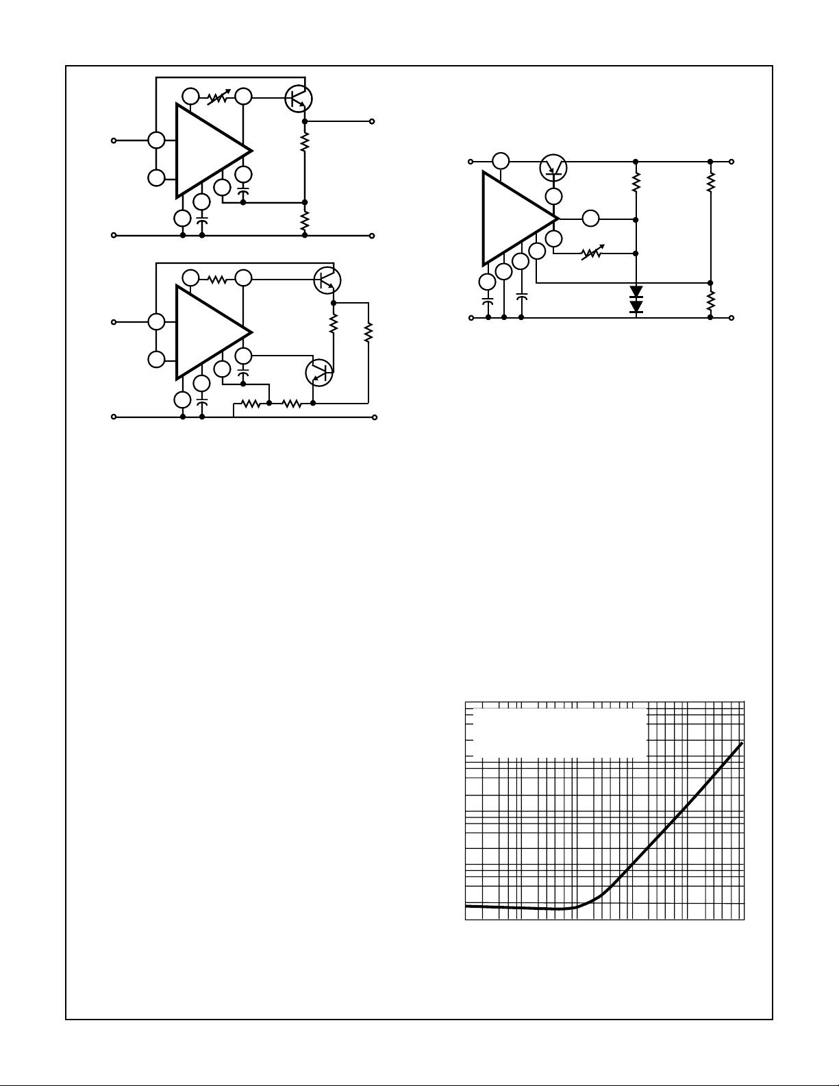
Figure 8 which shows the output impedance of the circuit of
Figure 7 as a function of frequency, illustrates the excellent
ripple-rejection characteristics of this circuit at frequencies
below 1kHz. Lower output impedances at the higher frequencies can be provided by connecting an appropriate
capacitor across the output voltage terminals. The addition
of a capacitor will, however, degrade the ability of the system
to react to transient-load conditions.
1000
INPUT VOLTAGE (V+I) = 15V
OUTPUT VOLTAGE (V+
AMBIENT TEMPERATURE (T
100
10
1
OUTPUT RESISTANCE (Ω)
0.1
0.01 0.1 1 10 100 1000
FIGURE 8. OUTPUT RESISTANCE vs FREQUENCY FOR
CIRCUIT OF FIGURE 7
) = 10V
O
) = 25oC
A
FREQUENCY (kHz)
O
11-55
Page 5
Application Note 6157
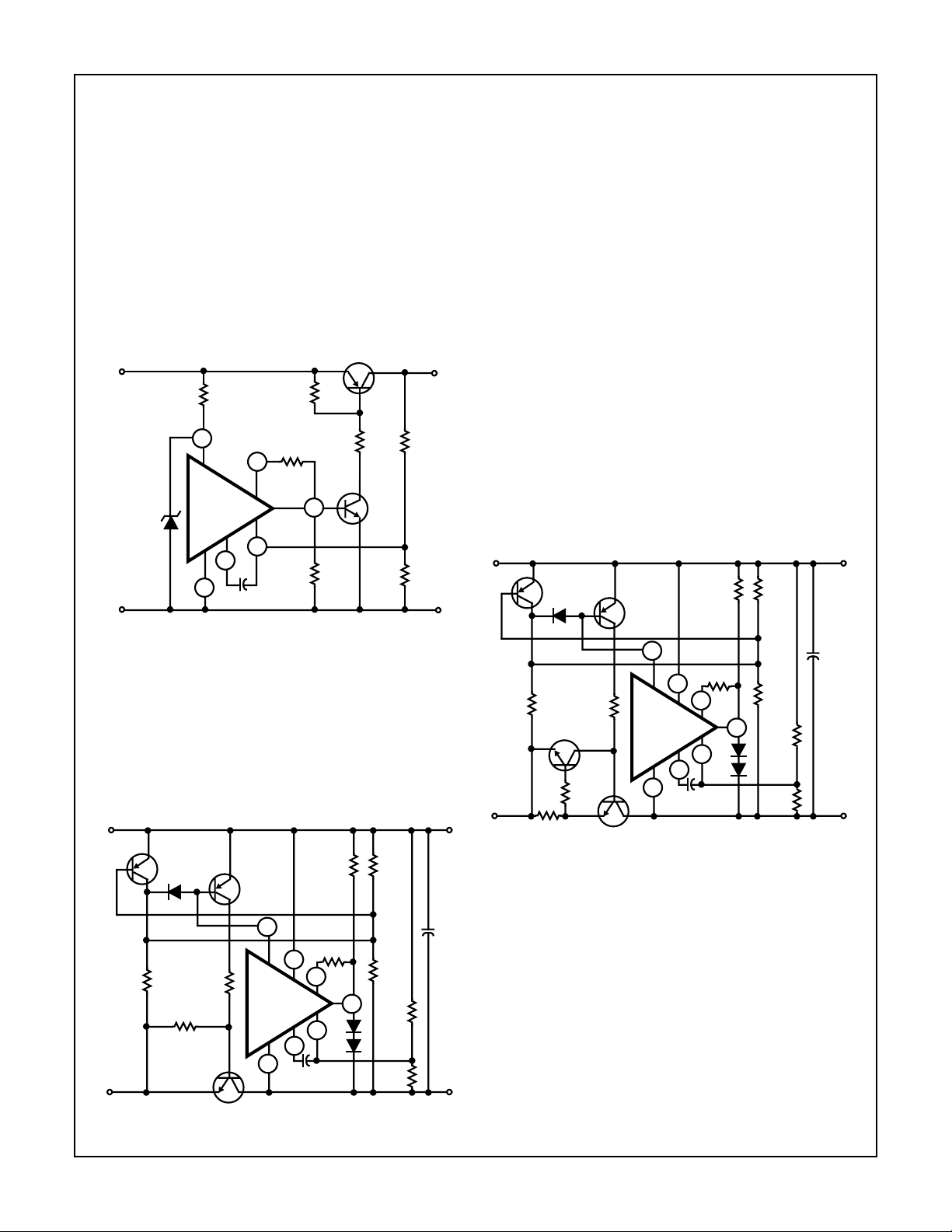
High Voltage Regulator
Figure 9 shows a circuit that uses the CA3085 as a voltage
reference and regulator control device for high-voltage
power supplies in which the voltages to be regulated are well
above the input-voltage ratings of the CA3085 series circuits.
The external transistors Q1 and Q2 require voltage ratings in
excess of the maximum input voltage to be regulated,
Series-pass transistor Q2 is controlled by the collector current of Q1, which in turn is controlled by the normally regulated current output supplied by the CA3085. The input
voltage for the CA3085 regulator at terminal 3 is supplied
through dropping resistor R3 and the clamping zener diode
D1. The values for resistor R1 and R2 are determined in
accordance with Equation 1.
220KΩ
10Ω
2N4036
4.7KΩ
2N3904
8
470Ω
+
R3
8.2KΩ
UNREG V
(e.g.120V)
I
DI
10V-15V
--
3
CA3085
7
4
1
6
0.01µF
FIGURE 9. HIGH VOLTAGE REGULATOR
Q1
Q2
R2
R1
REG
V
O
Negative Voltage Regulator
The CA3085 is used as a negative-supply voltage regulator
in the circuit shown in Figure 10. Transistor Q3 is the series
pass transistor. It should be noted that the CA3085 is effectively connected across the load side of the regulated system. Diode D1 is used initially in a “circuit-starter” function;
transistor Q2 “latches” D1 out of its starter-circuit function so
that the CA3085 can assume its role in controlling the pass
transistor Q3 by means of Q1.
+
2N3906
UNREG
-
Q2
IN914
D1
V
I
R3
4.7KΩ
220Ω
2N2102
Q1
2N3906
2
1KΩ
CA3085
4
Q3
3
1
6
7
0.005µF
10KΩ
10Ω
8
IN914
FIGURE 10. NEGATIVE VOLTAGE REGULATOR
1KΩ
12KΩ
R2
R1
5µF
REG
Operation of the circuit is as follows: current through R3 and
D1 provides base drive for Q1, which in turn provides base
drive for the pass-transistor Q3. By this means operating
potential for the CA3085 is developed between the collector of
Q3 (terminal 4 of the CA3085) and the positive supply-rail (terminal 3 of the CA3085). When the output voltage has risen
sufficiently to maintain operation of the CA3085 (approx.
7.5V), transistor Q2 is driven into conduction by the base drive
supplied from the 1KΩ-12KΩ voltage divider. As Q2 becomes
conductive, it diverts the base drive being supplied to Q1
through the R3-D1 path, and diode D1 ceases to conduct.
Under these conditions, base-current drive to Q1 through terminal 2 of the CA3085 regulates the base drive to Q3. Values
of R1 and R2 are determined in accordance with Equation 1.
+
The circuit shown in Figure 11 is similar to that of Figure 10,
except for the addition of a constant-current limiting circuit
consisting of transistor Q4, a 1KΩ resistor, and resistor R
When the load current increases above a particular design
value, the corresponding increase in the voltage drop across
resistor R
provides additional base drive to transistor Q4.
SCP
Thus, as transistor Q4 becomes increasingly conductive, its
collector current diverts sufficient base drive from Q3 to limit
the current in the pass transistor feeding the regulated load.
With the types of transistors shown in Figures 10 and 11,
maximum currents in the order of 5A can be regulated.
+
Q2
2N3906
D1
IN914
UNREG
V
I
R3
4.7KΩ
2N3904
1KΩ
-
R
+
SCP
Q4
Q1
2N3906
2
1KΩ
CA3085
4
Q3
2N5497
10KΩ
10Ω
3
1
8
6
7
0.005µF
PASS TRANSISTOR
IN914
FIGURE 11. NEGATIVE VOLTAGE REGULATOR WITH
CONSTANT CURRENT LIMITING CIRCUIT
High-Output-Current Voltage Regulator With “Foldback”
Current-Limiting (Also known as “Switch-Back”
Current-Limiting)
In high-current voltage regulators employing constant cur-
V
O
rent limiting (e.g., Figures 6 and 7), it is possible to develop
excessive dissipation in the series-pass transistor when a
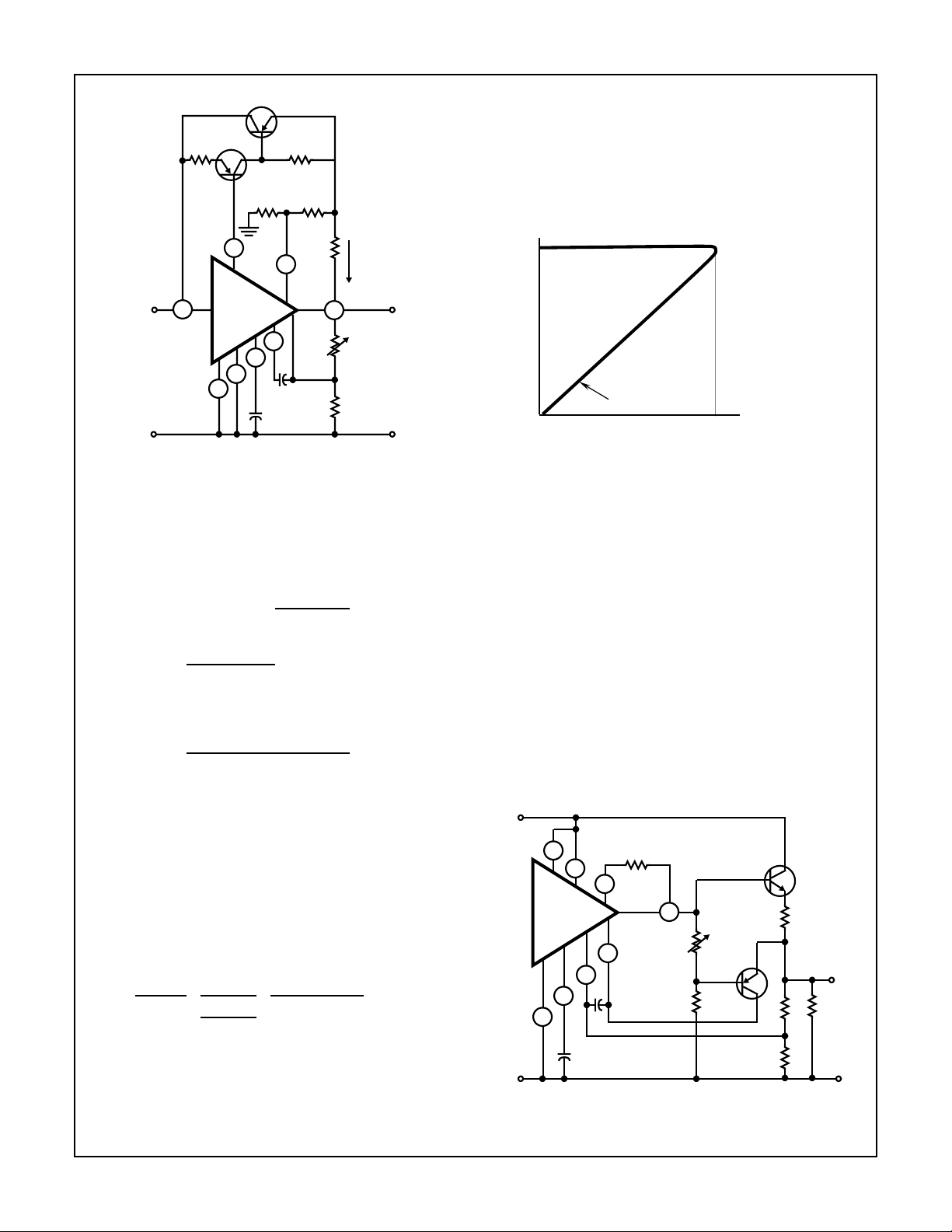
short circuit develops across the output terminals. This situation can be avoided by the use of the “foldback” current-limiting circuitry as shown in Figure 12. In this circuit, terminal 8
of the CA3085 senses the output voltage, and terminal 1 is
tied to a tap on a voltage-divider network connected
-
between the emitter of the pass-transistor (Q3) and ground.
The current-foldback trip-point is established by the value of
resistor R
SC
.
1KΩ
12KΩ
R2
R1
5µF
SCP
+
REG
V
O
-
.
11-56
Page 6
Application Note 6157
Q4
2N3772
Q2
+
UNREG
V
I
-
500Ω
3
2N4036
R3
2
CA3085
5
3
1.3Ω
RI
7
200Ω
1
6
0.001µF
2µF
460Ω
R2
8
1KΩ
R
SC
I
L
25KΩ
REG
V
+
O
-
FIGURE 12. HIGH OUTPUT CURRENT VOLTAGE REGULATOR
WITH “FOLDBACK” CURRENT LIMITING
The protective tripping action is accomplished by forwardbiasing Q15 in the CA3085 (see Figure 2). Conditions for
tripping circuit operation are defined by the following expressions:
V
BE(Q15)
V
SE(Q15)
(voltage at terminal 1) - (output voltage)
=
(VO + IL RSC)
=
[
If
(VO + ILRSC) K - VO = KVO + KILRSC - V
=
R1
R1 + R2
= K, then
and therefore
VO + V
RSC=
BE(Q15)
KI
L
R1
R1 + R2
- KV
O
]-V
(EQ. 3)
O
O
(EQ. 4)
Under load short-circuit conditions, terminal 8 is forced to
ground potential and current flows from the emitter of Q14 in
the CA3085, establishing terminal 1 at one V
-drop [≅0.7V]
SE
above ground and Q15 in a partially conducting state. The
current through Q14 necessary to establish this one V
SE
condition is the sum of currents flowing to ground through R1
and [R2 + R
can be ignored; therefore, the equivalent resistance R
]. Normally RSC is much smaller than R2 and
SC
eq
to
ground is the parallel combination of R1 and R2.
The Q14 current is then given by:
I
Q14
=
V
BE(Q15)
R
EQ
V
BE(Q15)
=
R1R2 1.3 x 0.46
0.7 [1.3 + 0.46]
=
R1 + R2 (EQ. 5)
2.06mA
This current provides a voltage between terminals 2 and 3
as follows:
V
2-3
Ω
= I
x 250Ω = 2.06 x 10-3 x 250 = 0.515V (EQ. 6)
Q14
The effective resistance between terminals 2 and 3 is 250Ω
because the external 500Ω resistor R3 is in parallel with the
internal 500Ω resistor R5. It should be understood that the
V
potential of 0.515V is insufficient to maintain the exter-
2-3
nal p-n-p transistor Q2 in conduction, and, therefore, Q3 has
no base drive. Thus the output current is reduced to zero by
the protective circuitry. Figure 13 shows the foldback characteristic typical of the circuit of Figure 12.
10
), (V)
O
OUTPUT VOLTAGE (V
0
2mA
OUTPUT CURRENT (I
), (A)
O
FIGURE 13. TYPICAL “FOLDBACK” CURRENT-LIMITING
CHARACTERISTIC FOR CIRCUIT OF FIGURE 12
INPUT VOLTAGE
(V
) = 15V
I
CURRENT TRIP
SET FOR 1A
An alternative method of providing “foldback” current-limiting
is shown in Figure 14. The operation of this circuit is similar
to that of Figure 12 except that the foldback-control transistor
Q2 is external to the CA3085 to permit added flexibility in
protection-circuit design.
Under low load conditions Q2 is effectively reverse-biased by
a small amount, depending upon the values of R3 and R4.
As the small amount, depending upon the values of R3 and
R4. As the load current increases the voltage drop across
R
increases, thereby raising the voltage at the base of Q1,
trip
and Q2 starts to conduct. As Q2 becomes increasingly conductive it diverts base current from transistors Q13 and Q14
in the CA3085, and thus reduces base drive to the external
pass-transistor Q1 with a consequent reduction in the output
voltage. The point at which current-limiting occurs, I
tnp
, is
calculated as follows:
V
= voltage at terminal 8 - VO (assuming a low value for R
BE(Q1)
+
UNREG
V
I
2
CA3085
4
3
5
2µF
5.6Ω
1
7
6
0.001µF
8
R3
R4
Q1 2N5497
PASS
TRANSISITOR
Q1
2N3906
R2
R1
FIGURE 14. HIGH-OUTPUT-CURRENT VOLTAGE REGULA-
TOR USING AUXILIARY TRANSISTOR TO
PROVIDE “FOLDBACK” CURRENT LIMITING
TRIP
R
TRIP
+
R
L
REG
V
O
)
--
11-57
Page 7
Application Note 6157
V
BE(Q2) =
voltage at terminal 8
=[VO + IL R
if K =
I
trip
R3 + R4
V
BE(Q2)
=
TRIP
R4
- K[VO + V
KR
+ V
BE(Q1)
][
, then the trip current is given by:
] + V
BE(Q1)
TRIP
(
O
R4
R3 + R4
R4
R3 + R4
- V
O
)
- V
O
]
(EQ. 7)
In the circuit in Figure 12 the load current goes to zero when
a short circuit occurs. In the circuit of Figure 14 the load current is significantly reduced but does not go to zero. The
value for I
I
SC =
is computed as follows:
SC
V
V
BE(Q2)
V
BE(Q2)
BE(Q2)
+
[
R2
V
BE(Q2)
+
[
R2
+ I
+ I
B(Q2)
B(Q2)
R
TRIP
]
]
R1 = V
R1 = V
BE(Q1)
BE(Q1)
+ ISCR
TRIP
(EQ. 8)
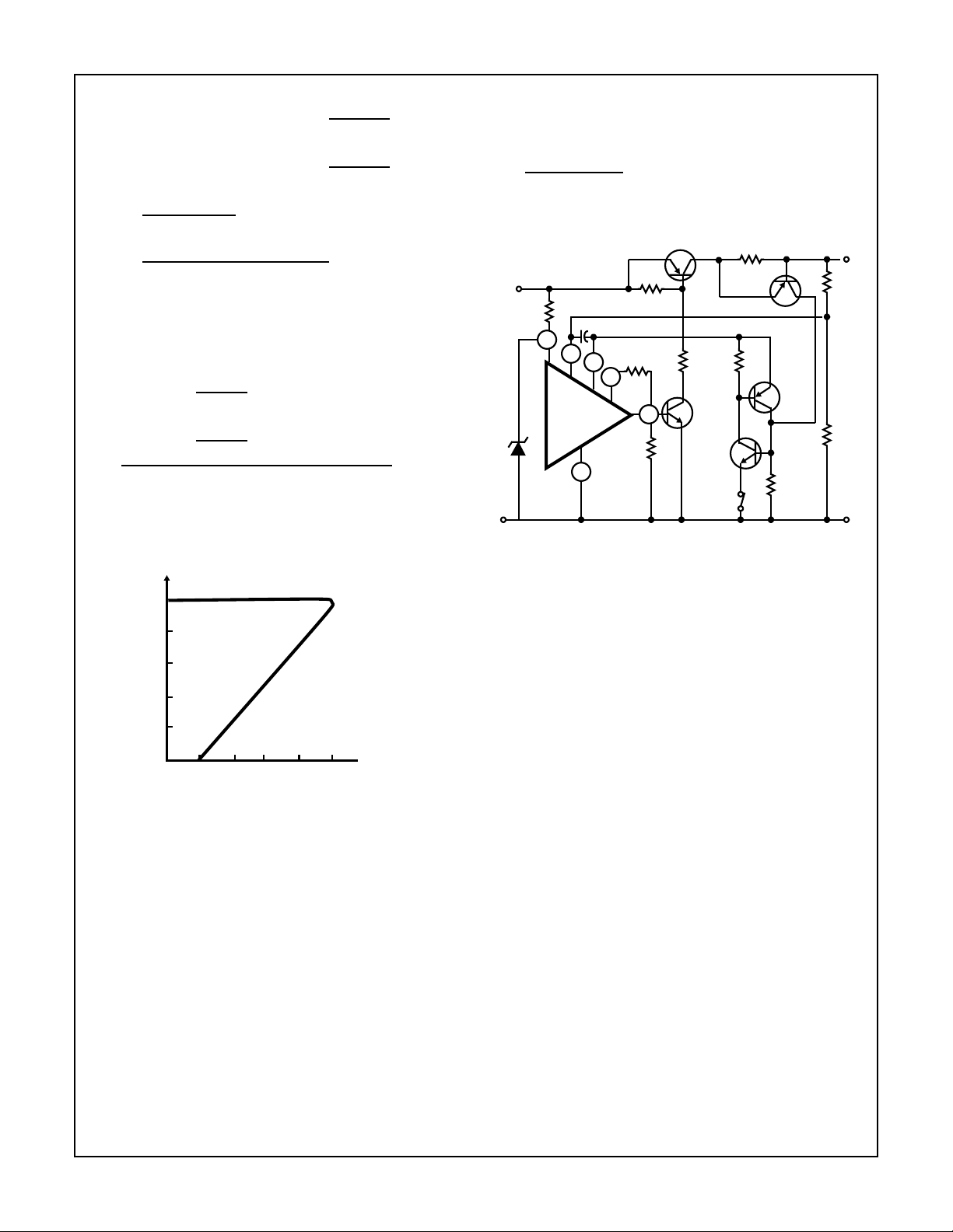
Figure 15 shows that the transfer characteristic of the load
current is essentially linear between the “trip-point” and the
“short-circuit” point.
10
8
6
4
OUTPUT VOLTAGE (V)
2
INPUT VOLTAGE (VI) = 15V
CURRENT TRIP SET FOR 500mA
The additional circuitry in the circuit of Figure 16 quickly
interrupts base drive to the pass transistor in event of load
fault. The point of current-trip is established as follows:
V
I
=
trip
+
UNREG
V
I
D1
10V-15V
-
FIGURE 16. HIGH-VOLTAGE REGULATOR INCORPORATING
BE(Q1)
R
SC
Q5
2N4036
1
18Ω
470Ω
220Ω
4.7Ω
8
Q4
2N3904
2N3904
8.2KΩ
0.01µF
3
6
7
CA3085
4
CURRENT “SNAP-BACK” PROTECTION
33KΩ
Q2
S1
(NC)
R
SC
2N4036
Q1
Q3
2N4036
33KΩ
(EQ. 9)
R2
REG
V
R1
+
O
-
Thus, when a sufficient voltage drop is developed across
R
, transistor Q1 becomes conductive and current flows
SC
into the base of Q2 so that it also becomes conductive. Transistor Q3, in turn, is driven into conduction, thereby latching
the Q2-Q3 combination (basic SCR action) so that it diverts
(through terminal 7) base drive from the output stage (Q13,
Q14) in the CA3085. By this means, base drive is diverted
from Q4 and the pass transistor Q5. To restore regulator
operation, normally closed switch S1 is momentarily opened
and unlatches Q2-Q3.
0
100
OUTPUT CURRENT (mA)
FIGURE 15. TYPICAL FOLDBACK CURRENT-LIMITING CHAR-
ACTERISTIC FOR CIRCUIT OF FIGURE 14
200
300
400
500
High-Voltage Regulator Employing Current “Snap-Back”
Protection
In high-voltage regulators (e.g., see Figure 9), “foldback” current-limiting cannot be used safely because the high voltage
across the pass transistor can cause second breakdown
despite the reduction in current flow. To adequately protect
the pass transistor in this type of high-voltage regulator, the
so-called “snap-back” method of current limiting can be
employed to reduce the current to zero in a few microseconds, and thus prevent second-breakdown destruction of the
device.
The circuit diagram of a high-voltage regulator employing
current “snap-back” protection is shown in Figure 16. The
basic regulator circuit is similar to that shown in Figure 9.
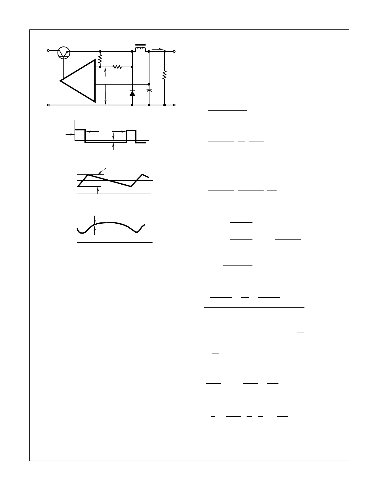
Switching Regulator
When large input-to-output voltage differences are necessary, the regulators described above are inefficient because
they dissipate significant power in the series-pass transistor.
Under these conditions, high-efficiency operation can be
achieved by using a switching-type regulator of the generic
type shown in Figure 17A. Transistor Q1 acts as a keyed
switch and operates in either a saturated or cut-off condition
to minimize dissipation. When transistor Q1 is conductive,
diode D1 is reversed-biased and current in the inductance
L1 increases in accordance with the following relationship:
t
1
1
i
=
Vdt
-- -
L
∫
L
t
0
11-58
(EQ. 10)
Page 8
Application Note 6157
I
C1
O
R
+
L
REG.
V
O
+
UNREG.
V
I
Q1
OP-AMP
L1
V
X
R2
V
+
V
REF
-
REF
R1
D1
-
FIGURE 17A. SELF-OSCILLATING SWITCHING REGULATOR
V
I
t
ON
O
FIGURE 17B. VOLTAGE AT POINT V
I
MAX
I
MIN
FIGURE 17C. INDUCTOR CURRENT I
REG. V
O
FIGURE 17D. OUTPUT VOLTAGE
FIGURE 17. SWITCHING REGULATOR AND ASSOCIATED
WAVEFORMS
∆V
t
OFF
FORWARD DROP OF D1
∆I
L
O
t
X
t
LI
V
REF
t
Where V is the voltage across the inductance L1. The current
through the inductance charges the capacitor C1 and supplies
current to the load. The output voltage rises until it slightly
exceeds the reference voltage V
. At this point the op-amp
ref
removes base drive to Q1 and the unregulated input voltage
V1 is “switched off”. The energy stored in the inductor L1 now
causes the voltage at V
to swing in the negative direction and
x
current flows through diode D1, while continuing to supply
current into the load R
. As the current in the inductor falls
L
below the load current, the capacitor C1 begins to discharge
and V
decreases. When VO falls slightly below the value of
O
V
, the op-amp turns on Q1 and the cycle is repeated. It
REF
should be apparent that the output voltage oscillates about
V
with an amplitude determined by R1 and R2. Actually,
REF
the value of V
V
when Q1 is conducting, to being slightly more negative
REF
than V
REF
varies from being slightly more positive than
REF
when D1 is conducting. The voltage and current
waveforms are shown in Figure 17B, C, and D.
Design Example
The following specifications are used in decomputations for
a switching regulator:
VI = 30V, VO = 5V, IO = 500mA,
switching frequency = 20kHz,
output ripple = 100mV
If it is assumed that transistor Q1 is in steady-state saturated
operation with a low voltage-drop, the current in the inductor
is given by Eq.10, as follows:
t1
1
i
L
Vdt
==
--
∫
L
t
0
VIV
–
O
------------------ -
t
ON
L
1
(EQ. 11)
When transistor Q1 is off, the current in the inductor is given
by:
iL ≅
(VO + VD1) t
L1
OFF
(EQ. 12)
From Equation 11,
(VI - VO).1.V
If i
L1 =
max
i
L
is 1.3 IL, then during ton the current in the inductor (iL)
will be 0.5A x 1.3 = 0.65A; therefore, ∆i
O
fV
I
= 0.15A.
L
(EQ. 13)
Substitution in Equation 13 yields
(30 - 5)
L1 =
0.15 (20 x 103)30
1
.
.5. 1.4mH (EQ. 14)
Current discharge from the capacitor C1 is given by:
iC =C
Thus, ∆iC=C
Since iC = iLand ∆t = t
C =
dv
dt
∆v
or C =
∆t ∆v
, then
OFF
∆iLt
OFF
∆v
∆IC∆t
(EQ. 15)
Substitution for the value of iL from Equation 13 yields
VI - V
O
ON
)
.1.
OFF
(
C =
L1 f
The total period T = t
t
=1-t
OFF
f
For optimum efficiency t
V
O
≅
(
Substitution for t
t
=1-
OFF
T ≅
)
V
I V
fV
(
in Equation 18 yields
on
V
O
(
)
I
V
O
(
V
∆v
+ tON, and T =
should be
on
V
O
)
I
1=1
(
ff
I
1 -
.t
OFF
)
(EQ. 16)
1
Therefore,
f
(EQ. 17)
1
f
V
O
)
V
I
(EQ. 18)
(EQ. 19)
11-59
Page 9
Application Note 6157
Substitution for ton in Equation 16 yields
C =
(V
I -VO
L
1
).1.V
fVIf
O
.1.(1 -
∆v
V
O
V
I
)
(EQ. 20)
Substitution of numerical values in Equation 20 produces the
following value for C:
30 - 5
1.4 x 10-320 x 10330 20 x 10
C =
1
.
5
.
10
1
.
-1
3
.(1 -
30
5
)
= 63µF
A switching-regulator circuit using the CA3085 is shown in
Figure 18. The values of L and C (1.5mH and 50mF, respectively) are commercially available components having values
approximately equal to the computed values in the previous
design example.
2N4036
V
I
R
50µF
50V
LIMIT
3
4
----------------------------- -
=
1.2 I
L
2
5
CA3085A
7
0.01µF
40V
0.7
MAX
()
1MΩ
L
1
6
V
= V
O
I
C1
R
LIMIT
8
R2
R1
REF.
R1 R1+
------------------ -
R1
IN4001
D1
V
O
REG. I
L
R
3
7
0.001µF
L
1
R
SC
2N3772
8
6
R1
UNREG.
NEG. V
2
CA3085A
4
(-)
I
(B)
HIGH-CURRENT REGULATOR
FIGURE 19B. HIGH-CURRENT REGULATOR
FIGURE 19. CONSTANT CURRENT REGULATORS
The actual regulated current, reg IL is the sum of the quiescent regulator current and the current through R1, i.e.,
reg IL = I
QUIESCENT
+ I
R1
Figure 19B shows a high-current regulator using the CA3085
in conjunction with an external n-p-n transistor to regulate
currents up to 3A. In this circuit the quiescent regulator current does not flow through the load and the output current
can be directly programmed by R1, i.e.,
V
Reg IL =
REF
R1
With this regulator currents between 1mA and 3A can be
programmed directly. At currents below 1mA inaccuracies
may occur as a result of leakage in the external transistor.
A Dual-Tracking Voltage Regulator
FIGURE 18. TYPICAL SWITCHING REGULATOR CIRCUIT
Current Regulators
The CA3085 series of voltage regulators can be used to provide a constant source or sink current. A regulated-current
supply capable of delivering up to 100mA is shown in Figure
19A . The regulated load current is controlled by R1 because
the current flowing through this resistor must establish a voltage difference between terminals 6 and 4 that is equal to the
internal reference voltage developed between terminals 5
and 4.
UNREG. V
3
7
0.001µF
CA3085A
6
8
1
R
SC
R1
FIGURE 19A. CURRENT REGULATOR
2
4
I
QUIES.
(+) R
REG. I
I
L
L
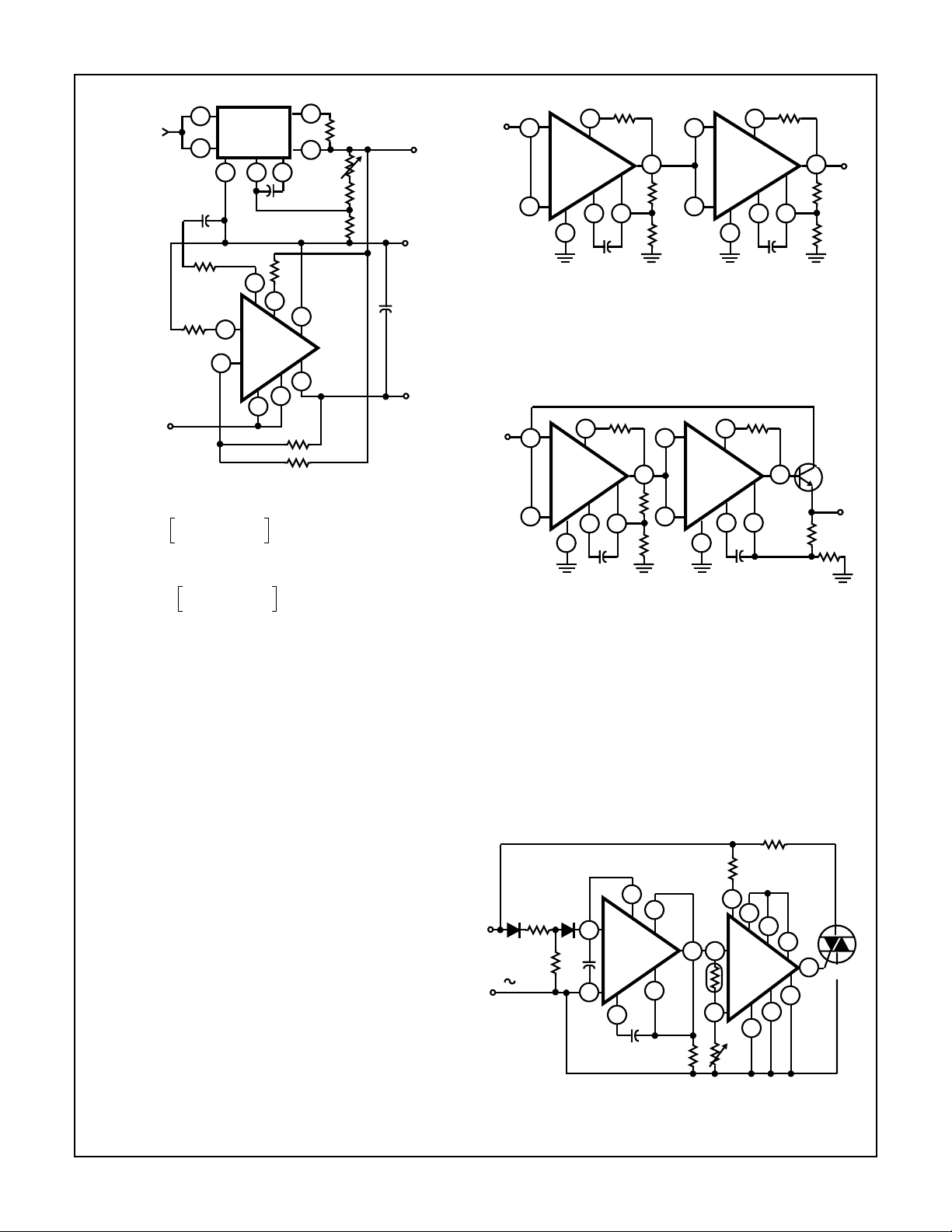
A dual-tracking voltage regulator using a CA3085 and a
CA3094A is shown in Figure 20. The CA3094A is basically an
op-amp capable of supplying 100mA of output current. Specifications for the CA3094A appear in datasheet file number 598.
The positive output voltage is regulated by a CA3085 operating
in a configuration essentially similar to that described in connection with Figure 3. Resistor R is used as a vernier adjustment of
output voltage. The negative output voltage is regulated by the
CA3094A, which is “slaved” to the regulated positive voltage supplied by the CA3085. It should be noted that the non-inverting
input of the CA3094A and the negative supply terminal of the
CA3085 are connected to a common ground reference. The
“slaving” potential for the CA3094A is derived from an accurate
1:1 voltage-divider network comprised of two 10KΩ resistors
connected between the +15V and the -15V output terminals. The
junction of these two resistors is connected to the inverting input
of the CA3094A. The voltage at this junction is compared with
the voltage at the non-inverting input, and the CA3094A then
automatically adjusts the output current at the negative terminal
to maintain a negative regulated output voltage essentially equal
to the regulated positive output voltage. Typical performance data
for this circuit are shown in Figure 20.
11-60
Page 10
Application Note 6157
V+ INPUT
(NOTE 1)
V- INPUT
(NOTE 2)
REGULATION:
MAX. LINE =
MAX. LOAD =
2
CA3085A
VOLTAGE
REG.
3
4 6 7
REF.
0.0056µF
100Ω
5.1k
∆V
------------------------------------------------------- -
V
INITIAL
()
OUT
------------------------------------------------------- -
V
()
OUT
1.6V
2
CA3094A
3
OUT
∆V
OUT
INITIAL
0.01µF
1
4
2
6
∆V
∆V
MAX. I
1
8
5KΩ
R
10KΩ
1.5Ω
200KΩ
200KΩ
7
8
10KΩ
±1%
10KΩ
±1%
X 100 = 0.075%/V
IN
X 100 = 0.075%/V
(IL FROM 1µA TO 50mA)
IN
5.6Ω
OUT
= 100mA
COMMON
0.03µF
-15V REG.
OUT
+15V
REG.
OUTPUT
RETURN
OUTPUT
NOTE:
1. V+ Input Range = 19V to 30V for 15V Output
2. V- Input Range = -16V to -30V for -15V Output
FIGURE 20. DUAL-VOLTAGE TRACKING REGULATOR
The basic circuit of Figure 20 can be modified to regulate dissimilar positive and negative voltages (e.g., +15V, -5V) by
appropriate selection of resistor ratios in the voltage-divider
network discussed previously. As an example, to provide
tracking of the -15V and -5V regulated voltages with the circuit
of Figure 20, it is only necessary to replace the 10KΩ resistor
connected between terminals 3 and 8 of the CA3094A with a
3.3
KΩ resistor.
Regulators With High Ripple Rejection
When the reference-voltage source in the CA3085 is adequately filtered, the typical ripple rejection provided by the circuit is 56dB. It is possible to achieve higher ripple-rejection
performance by cascading two stages of the CA3085, as
shown in Figure 21. The voltage-regulator circuit in Figure 21A
provides 90dB of ripple rejection. The output voltage is adjustable over the range from 1.8V to 30V by appropriate adjustment
of resistors R1 and R2. Higher regulated output currents up to
1A can be obtained with this circuit by adding an external n-p-n
transistor as shown in Figure 21B.
UNREG.
V
I
2
40V
3
LOAD REG. <0.1% VOFOR LOAD CURRENTS UP TO 50mA
1
5.6Ω
CA3085A
7 6
4
0.001µF
90dB RIPPLE REJECTION
LINE REG. <0.0001%/ V
RANGE FROM 1.8V TO 30V
V
O
8
21KΩ
1KΩ
2
3
CA3085A
4
I
1
5.6Ω
7 6
0.001µF
8
REG.
V
R2
R1
O
FIGURE 21A. VOLTAGE REGULATOR WITH HIGH RIPPLE
REJECTION
UNREG
V
40V
I
2
3
1
CA3085A
7
4
0.001µF
4Ω
2
8
21KΩ
6
3
1KΩ
1
CA3085A
7 6
4
5.6Ω
0.001µF
2N3772
8
R2
REG.
R1
V
O
FIGURE 21B. HIGH-CURRENT VOLTAGE REGULATOR WITH
HIGH RIPPLE REJECTION
The CA3085 As A Power Source For Sensors
Certain types of sensor applications require a regulated power
source. Additionally, low-impedance sensors can consume significant power. An example of a circuit with these requirements,
in which a CA3085 provides regulated power for a low-impedance sensor and the CA3059 zero-voltage switch, is shown in
Figure 22. Terminal 12 on the CA3059 provides the ac triggersignal which actuates the zero-voltage switch synchronously
with the power line to control the load-switching triac. Specifications for the CA3059 appear in datasheet file number 490.
RL
10KΩ
IN4001
120V
60
600Ω
20W
100Ω
IN4001
3
250µF
4
2
CA3085A
7
0.001µF
1
6
1KΩ
100Ω
8 2
2.8KΩ
8
12
R
200Ω
9
10
CA3085A
7
P
MT2
11
4
MT1
G
5
8
FIGURE 22. VOLTAGE REGULATOR FOR SENSOR AND ZERO-
VOLTAGE SWITCH
11-61
Page 11
Application Note 6157
The CA3085 As A General-Purpose Amplifier
As described above, the CA3085 series regulators contain a
high-gain linear amplifier having a current-output capability
up to 100mA. The premium type (CA3085B) can operate at
supply voltages up to 50V. When equipped with an appropriate radiator or heat sink, the TO-5 package of these devices
can dissipate up to 1.6W at 55
o
C. A very stable internal voltage-reference source is used to bias the high-gain amplifier
and/or provide an external voltage-reference despite
extreme temperature or supply-voltage variations. These
factors, plus economics, prompt consideration of this circuit
for general-purpose uses, such as amplifiers, relay controls,
signal-lamp controls, and thyristor firing.
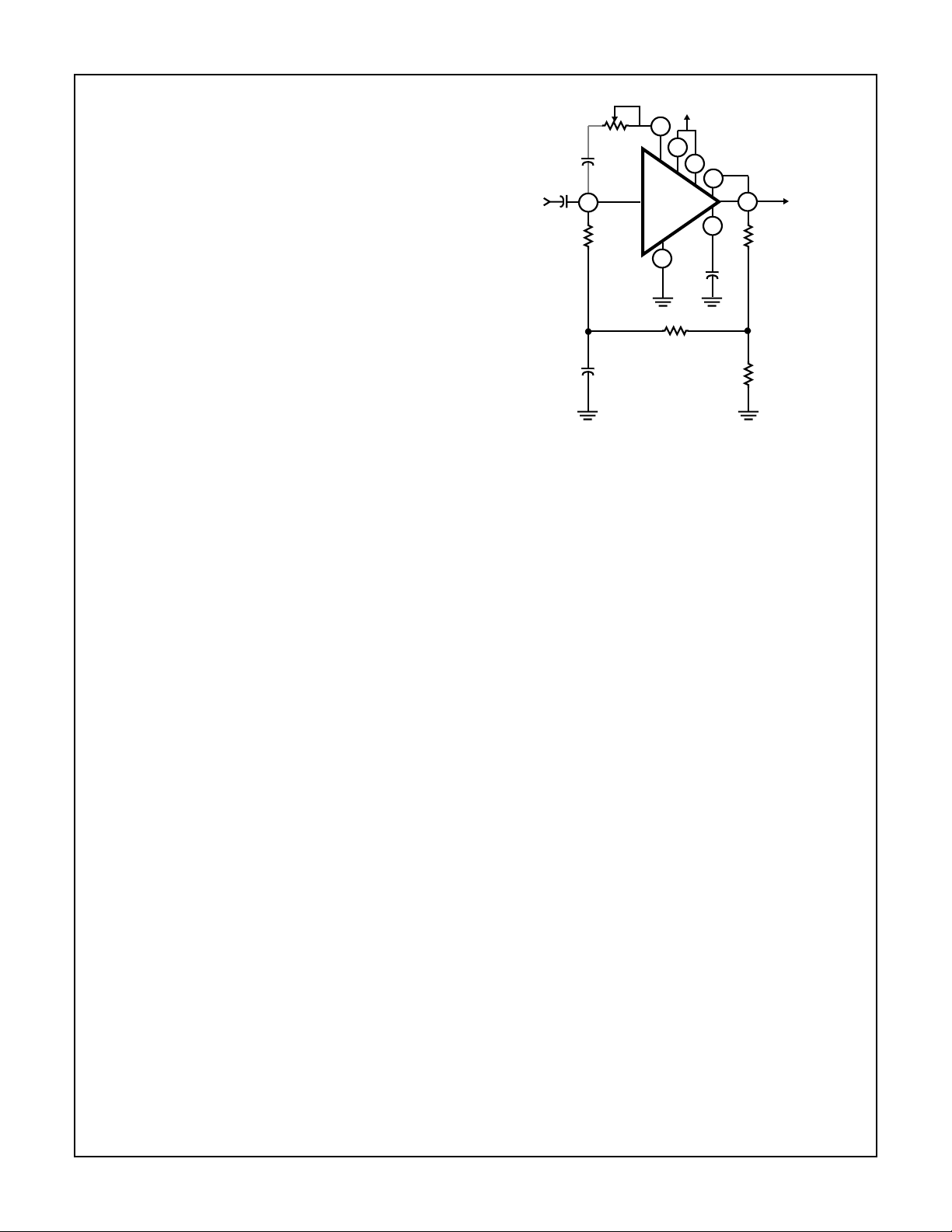
As an example, Figure 23 shows the application of the
CA3085 in a general-purpose amplifier. Under the conditions
shown, the circuit has a typical gain of 70bB with a flat
response to at least 100kHz without the RC network connected between terminals 6 and 7. The RC network is useful
as a tone control or to “roll-off” the amplifier response for
other reasons. Current limiting is not used in this circuit. The
network connected between terminals 8 and 6 provides both
dc and ac feedback. This circuit is also applicable for directly
driving an external discrete n-p-n power transistor.
R
C
INPUT
SIGNAL
FIGURE 23. GENERAL-PURPOSE AMPLIFIER USING CA3085A
6
680Ω
10µF
+12V
7
3
CA3085A
4
680Ω
2
1
8
5
2µF
OUTPUT
3KΩ
1KΩ
11-62
 Loading...